Abstract
Disclosed herein is a circuit substrate that includes a coil component mounted on the substrate having first and second land patterns and first and second dummy land patterns. The coil component includes a first signal terminal and a first dummy terminal which are provided on the first flange part, a second signal terminal and a second dummy terminal which are provided on the second flange part, and a wire wound around the winding core part and whose one end and other end are connected respectively to the first signal terminal and the second signal terminal. The coil component is mounted on the substrate such that the first and second signal terminals are connected respectively to the first and second land patterns and that the first and second dummy patterns are connected respectively to the first and second dummy land patterns.
Claims (9)
1. A circuit substrate comprising: a substrate; and a chip-type coil component surface-mounted on the substrate, wherein the substrate includes: first and second signal lines; first and second land patterns connected respectively to the first and second signal lines; and first and second dummy land patterns which are in a floating state, wherein the coil component includes: a drum-shaped core having first and second flange parts and a winding core part positioned between the first and second flange parts; a first signal terminal and a first dummy terminal which are provided on the first flange part; a second signal terminal and a second dummy terminal which are provided on the second flange part; and a wire wound around the winding core part and whose one end and other end are connected respectively to the first signal terminal and the second signal terminal, and wherein the coil component is mounted on the substrate such that the first and second signal terminals are connected respectively to the first and second land patterns and that the first and second dummy patterns are connected respectively to the first and second dummy land patterns.
Show 8 dependent claims
2. The circuit substrate as claimed in claim 1 , wherein each of the first and second dummy land patterns is an independent pattern not connected to any other pattern.
3. The circuit substrate as claimed in claim 1 , wherein the first and second land patterns are smaller in effective area than the first and second dummy land patterns.
4. The circuit substrate as claimed in claim 3 , wherein the first and second land patterns are the same in outer size as the first and second dummy land patterns, and wherein each of the first and second land patterns has a reduced effective area due to a presence of cuts formed therein.
5. The circuit substrate as claimed in claim 1 , wherein the first land pattern and the second dummy land pattern face each other in an axial direction, and wherein the second land pattern and the first dummy land pattern face each other in the axial direction.
6. The circuit substrate as claimed in claim 1 , wherein each of the first and second land patterns has a slit.
7. The circuit substrate as claimed in claim 6 , wherein each of the first and second dummy land patterns is a solid pattern having no slit.
8. The circuit substrate as claimed in claim 1 , wherein each of the first and second land patterns has a plurality of slits extending in an axial direction.
9. The circuit substrate as claimed in claim 1 , wherein the substrate further includes a ground pattern that overlaps the first and second land patterns and the first and second dummy land patterns.
Full Description
Show full text →
BACKGROUND OF THE INVENTION
Field of the Invention
The present invention relates to a circuit substrate and, more particularly, to a circuit substrate on which a chip-type coil component is surface-mounted.
Description of Related Art
JP 2008-140903A discloses a structure in which a pair of terminal electrodes of a coil component mounted on a substrate is connected to a signal line and another pair of terminal electrodes of the coil component is connected to a ground pattern. This allows the coil component to function as an LC composite component and reduces an insertion loss.
However, in the mounting structure described in JP 2008-140903A, a capacitance between the signal line and the ground increases to disadvantageously reduce impedance in a high frequency region.
SUMMARY
It is therefore an object of the present invention is to suppress a reduction in impedance in a high frequency region in a circuit substrate on which a chip-type coil component is surface-mounted.
A circuit substrate according to the present invention includes a substrate and a chip-type coil component surface-mounted on the substrate. The substrate includes first and second signal lines, first and second land patterns connected respectively to the first and second signal lines, and first and second dummy land patterns which are in a floating state. The coil component includes: a drum-shaped core having first and second flange parts and a winding core part positioned between the first and second flange parts; a first signal terminal and a first dummy terminal which are provided on the first flange part; a second signal terminal and a second dummy terminal which are provided on the second flange part; and a wire which is wound around the winding core part and whose one end and the other end are connected respectively to the first signal terminal and the second signal terminal. The coil component is mounted on the substrate such that the first and second signal terminals are connected respectively to the first and second land patterns and that the first and second dummy patterns are connected respectively to the first and second dummy land patterns.
According to the present invention, the dummy land patterns are in a floating state, so that as compared to a case where the land pattern and dummy land pattern are short-circuited, a capacitance between the land pattern and the ground is reduced. This can suppress a reduction in impedance in a high-frequency region. In addition, since the dummy land pattern is connected to the dummy terminal, sufficient mounting strength of the coil component with respect to the substrate can be ensured.
In the present invention, the first and second dummy land patterns may each be an independent pattern not connected to any other pattern. This can prevent the occurrence of noise due to the presence of the dummy land pattern.
In the present invention, the first and second land patterns may be smaller in effective area than the first and second dummy land patterns. This can further reduce a capacitance between the land pattern and the ground. In this case, the first and second land patterns may be the same in outer size as the first and second dummy land patterns and may each have a reduced effective area due to the presence of cuts formed therein. This can ensure sufficient connection strength between the land pattern and the signal terminal through a solder.
As described above, according to the present invention, a reduction in impedance in a high frequency region can be suppressed in a circuit substrate on which a chip-type coil component is surface-mounted.
BRIEF DESCRIPTION OF THE DRAWINGS
The above and other objects, features and advantages of this invention will become more apparent by reference to the following detailed description of the invention taken in conjunction with the accompanying drawings, wherein:
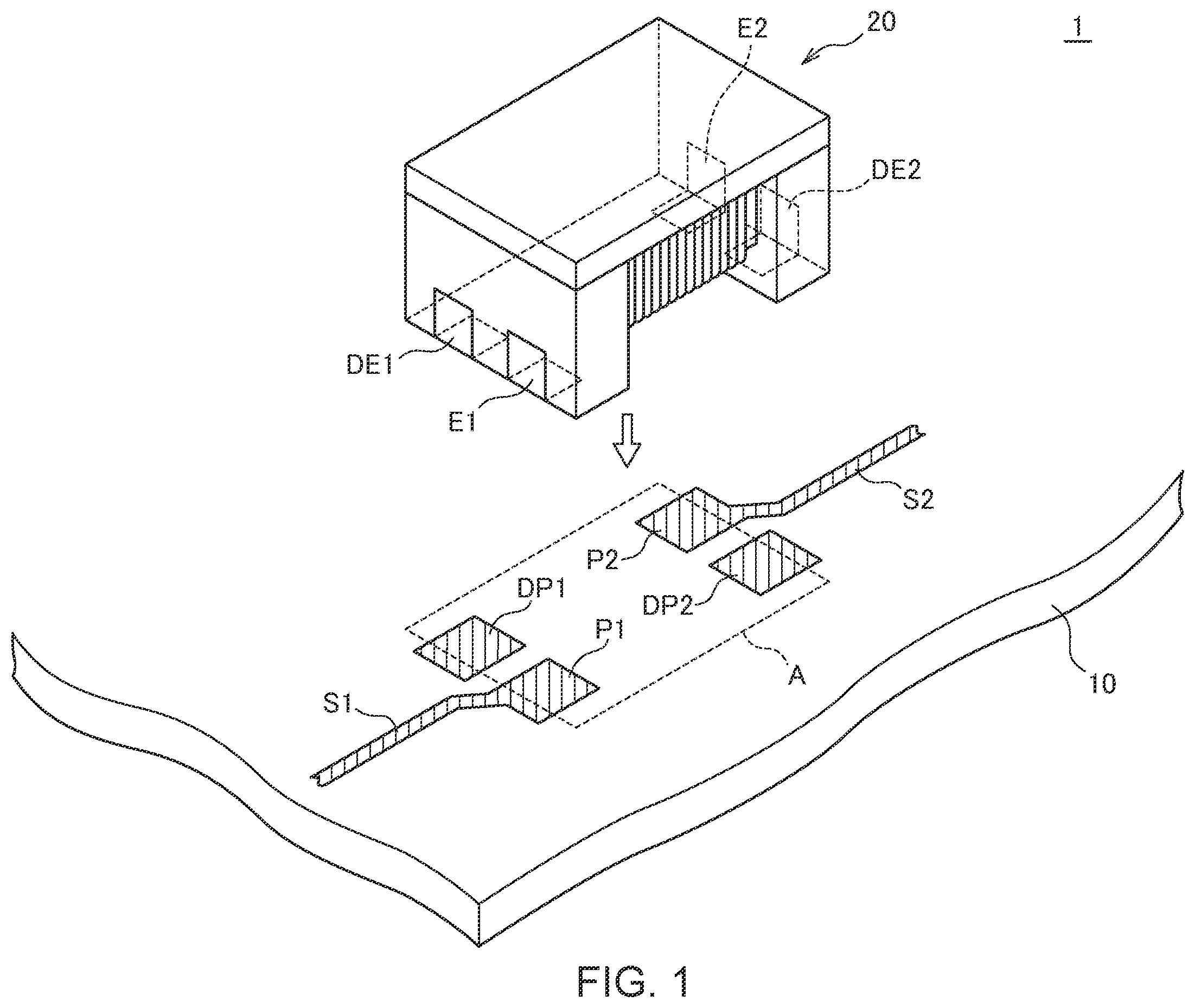
is a schematic exploded perspective view illustrating the outer appearance of a circuit substrate 1 according to a preferred embodiment of the present invention;
is a schematic perspective view illustrating the outer appearance of the coil component 20 ;
is a schematic cross-sectional view of the circuit substrate 1 ;
is an equivalent circuit diagram of the coil component 20 in a state of being mounted on the substrate 10 ;
is a graph for explaining effects of the present embodiment, in which the solid curve indicates characteristics of the coil component 20 in a state of being mounted on the substrate 10 , and the dashed curve indicates characteristics of the coil component 20 when the land patterns P 1 , P 2 and the dummy land patterns DP 1 , DP 2 are integrated respectively with each other;
is a schematic plan view illustrating a pattern arrangement on the substrate 10 according to a first modification; and
is a schematic plan view illustrating the pattern layout on the substrate 10 according to a second modification.
DETAILED DESCRIPTION OF THE EMBODIMENTS
Preferred embodiments of the present invention will now be explained in detail with reference to the drawings.
is a schematic exploded perspective view illustrating the outer appearance of a circuit substrate 1 according to a preferred embodiment of the present invention.
As illustrated in , the circuit substrate 1 according to the present embodiment includes a substrate 10 and a chip-type coil component 20 surface-mounted in a component mounting area A defined on the substrate 10 . There are provided on the surface of the substrate 10 signal lines S 1 and S 2 , land patterns P 1 and P 2 connected respectively to the signal lines S 1 and S 2 , and dummy land patterns DP 1 and DP 2 . The land patterns P 1 , P 2 and dummy land patterns DP 1 , DP 2 are all positioned in the component mounting area A. The dummy land patterns DP 1 and DP 2 are each an independent pattern (electrically floating pattern) not connected to any other pattern. In the example of , the land pattern P 1 and dummy land pattern DP 2 are disposed opposite to each other, and the land pattern P 2 and dummy land pattern DP 1 are disposed opposite to each other. In other words, the land patterns P 1 and P 2 are positioned diagonally to each other, and the dummy land patterns DP 1 and DP 2 are positioned diagonally to each other.
is a schematic perspective view illustrating the outer appearance of the coil component 20 .
As illustrated in , the coil component 20 includes: a drum-shaped core 30 having flange parts 31 , 32 and a winding core part 33 ; a plate-shaped core 40 fixed to the flange parts 31 and 32 ; a signal terminal E 1 and a dummy terminal DE 1 which are provided on the flange part 31 ; a signal terminal E 2 and a dummy terminal DE 2 which are provided on the flange part 32 ; and a wire W wound around the winding core part 33 . The wire W is a coated conductive wire having a good conductor such as copper as a core material.
The drum-shaped core 30 is a drum-shaped block made of a high permeability material such as ferrite and has a structure obtained by integrating the flange parts 31 , 32 and the winding core part 33 provided therebetween. The plate-shaped core 40 is a plate-shaped block also made of a high permeability material such as ferrite. The drum-shaped core 30 and the plate-shaped core 40 are fixed to each other through an adhesive or the like. One end of the wire W is connected to the signal terminal E 1 , and the other end thereof is connected to the signal terminal E 2 . The dummy terminals DE 1 and DE 2 are connected with no wire. The signal terminals E 1 , E 2 and dummy terminals DE 1 , DE 2 may each be made of a silver paste fired on the drum-shaped core 30 or may each be constituted by a terminal fitting bonded to the drum-shaped core 30 .
The coil component 20 is mounted on the substrate 10 such that the signal terminals E 1 and E 2 are connected respectively to the land patterns P 1 and P 2 and that the dummy terminals DE 1 and DE 2 are connected respectively to the dummy land patterns DP 1 and DP 2 . The connection between the signal terminal (E 1 , E 2 ) and the dummy terminal (DE 1 , DE 2 ) and the connection between the land pattern (P 1 , P 2 ) and the dummy land pattern (DP 1 , DP 2 ) are each made through a solder 50 as illustrated in the cross-sectional view of .
As illustrated in , a ground pattern G is provided inside the substrate 10 at a position overlapping the land patterns P 1 , P 2 and dummy land patterns DP 1 , DP 2 . This generates a stray capacitance between the land and dummy land patterns (P 1 , P 2 , DP 1 , DP 2 ) and the ground pattern G.
is an equivalent circuit diagram of the coil component 20 in a state of being mounted on the substrate 10 .
As illustrated in , the coil component 20 can be represented by an equivalent circuit in which an inductance component Ls, a capacitance component Cp, and a resistance component Rp are connected in parallel. In a state where the coil component 20 is mounted on the substrate 10 , a stray capacitance component Cpad generated between the land patterns P 1 , P 2 and the ground pattern G is added. On the other hand, the stray capacitance generated between the dummy land patterns DP 1 and DP 2 is not included in the stray capacitance component Cpad since the land pattern P 1 and the dummy land pattern DP 1 are isolated from each other, and the land pattern P 2 and the dummy land pattern DP 2 are isolated from each other. This reduces the stray capacitance component Cpad to suppress a reduction in impedance in a high frequency region. Further, since the dummy terminals DE 1 , DE 2 and the dummy land patterns DP 1 , DP 2 are respectively connected to each other through the solder 50 , sufficient mounting strength is provided to the coil component 20 .
is a graph for explaining effects of the present embodiment, in which the solid curve indicates characteristics of the coil component 20 in a state of being mounted on the substrate 10 (present embodiment), and the dashed curve indicates characteristics of the coil component 20 when the land patterns P 1 , P 2 and the dummy land patterns DP 1 , DP 2 are integrated respectively with each other (comparative example). As can be seen from , in a low frequency region, there is almost no difference in impedance between the circuit substrate 1 according to the present embodiment and the circuit substrate according to the comparative example, whereas in a high frequency region, the circuit substrate 1 according to the present embodiment exhibits higher impedance.
is a schematic plan view illustrating a pattern arrangement on the substrate 10 according to a first modification.
The pattern layout according to the first modification illustrated in differs from the pattern layout according to the above embodiment in that the land patterns P 1 and P 2 are disposed opposite to each other, and the dummy land patterns DP 1 and DP 2 are disposed opposite to each other. In this case, in the coil component 20 to be mounted on the substrate 10 , the wire connection positions need to be changed. Specifically, the positions of the signal terminal E 1 and dummy terminal DE 1 in are interchanged. As exemplified by the first modification, the layout of the land patterns P 1 , P 2 and dummy land patterns DP 1 , DP 2 is not particularly limited.
is a schematic plan view illustrating the pattern layout on the substrate 10 according to a second modification.
In the second modification illustrated in , the land patterns P 1 and P 2 each have a plurality of slit-shaped cuts. The land pattern (P 1 , P 2 ) and the dummy land pattern (DP 1 , DP 2 ) have the same outer size; however, since the presence of the slit-shaped cuts makes the effective area of the land pattern (P 1 , P 2 ) smaller than that of the dummy land pattern (DP 1 , DP 2 ). The effective area herein refers to the area of a part where the conductor pattern exists. By thus reducing the effective areas of the land patterns P 1 and P 2 , the stray capacitance component Cpad generated between the land patterns P 1 , P 2 and the ground pattern G is further reduced, thereby further improving impedance in a high-frequency region. In addition, the outer size of the land patterns P 1 and P 2 is maintained, so that connection strength by the solder 50 can be ensured.
While the preferred embodiment of the present invention has been described, the present invention is not limited to the above embodiment, and various modifications may be made within the scope of the present invention, and all such modifications are included in the present invention.
Figures (4)
Citations
This patent cites (8)
- US6087921
- US2005/0057334
- US2008/0309445
- US2016/0322706
- US2016/0323019
- US2018/0226181
- US2002-261430
- US2008-140903