Abstract
A semiconductor memory device includes a first chip, a second chip, and a multiple of bonding pads. The first chip has a multiple of memory pillars that penetrate a multiple of wiring layers in a first direction. The second chip is bonded to the first chip. The multiple of bonding pads are provided at a bonding face between the first chip and the second chip. The multiple of bonding pads include a first bonding pad that electrically connects a first memory pillar among the multiple of memory pillars to one of a multiple of transistors, and a second bonding pad that neighbors the first bonding pad when seen from the first direction, and which electrically connects a second memory pillar among the multiple of memory pillars to one of the multiple of transistors. The second memory pillar does not neighbor the first memory pillar when seen from the first direction.
Claims (18)
1. A semiconductor memory device, comprising: a first chip having a plurality of wiring layers stacked in a first direction, and a plurality of memory pillars extending into the plurality of wiring layers in the first direction; a second chip having a semiconductor substrate and a plurality of transistors provided on the semiconductor substrate, the second chip bonded to the first chip; and a plurality of bonding pads provided at a bonding face between the first chip and the second chip, wherein the plurality of bonding pads include: a first bonding pad electrically connecting a first memory pillar among the plurality of memory pillars to one of the plurality of transistors, and a second bonding pad adjacent the first bonding pad when seen from the first direction, the second bonding pad electrically connecting a second memory pillar among the plurality of memory pillars to one of the plurality of transistors, and wherein the second memory pillar is not adjacent the first memory pillar when seen from the first direction.
7. A semiconductor memory device, comprising: a first chip having a plurality of wiring layers stacked in a first direction and a plurality of memory pillars penetrating the plurality of wiring layers in the first direction; a second chip having a semiconductor substrate and a plurality of transistors provided on the semiconductor substrate, the second chip being bonded to the first chip; and a plurality of bonding pads provided at a bonding face between the first chip and the second chip, wherein the plurality of bonding pads include: a first bonding pad electrically connecting a first memory pillar among the plurality of memory pillars to one of the plurality of transistors, and a second bonding pad electrically connecting a second memory pillar among the plurality of memory pillars, the second bonding pad adjacent the first memory pillar when seen from the first direction, to one of the plurality of transistors, and wherein the second bonding pad is not adjacent the first bonding pad when seen from the first direction.
Show 16 dependent claims
2. The semiconductor memory device according to claim 1 , wherein the first chip further includes a plurality of bit lines disposed below the plurality of memory pillars, the plurality of bit lines (i) extending in a second direction intersecting the first direction, and (ii) arranged in a third direction intersecting the first direction and the second direction, the plurality of bit lines having (i) a first bit line connecting the first memory pillar to the first bonding pad and (ii) a second bit line connecting the second memory pillar to the second bonding pad, and at least seven of the plurality of bit lines arranged between the first bit line and the second bit line in the third direction.
3. The semiconductor memory device according to claim 2 , wherein the plurality of bonding pads are disposed sequentially in the third direction, and in a fourth direction opposite to the third direction, such that the at least seven bit lines are arranged between the bit lines to which the bonding pads are connected.
4. The semiconductor memory device according to claim 2 , wherein multiple bonding pads are disposed sequentially in the third direction such that the at least seven bit lines are arranged between the bit lines to which the bonding pads are connected.
5. The semiconductor memory device according to claim 2 , wherein each of the plurality of bonding pads is connected to a respective one of the plurality of bit lines via a first via plug, a wiring layer, and a second via plug, and the second via plugs connected to the adjacent abonding pads are disposed in the wiring layer such that that the at least seven bit lines are arranged between the bit lines to which the second via plugs are connected.
6. The semiconductor memory device according to claim 1 , wherein the first chip is an array chip including a memory cell array, and the second chip is a circuit chip including a control circuit configured to control the array chip.
8. The semiconductor memory device according to claim 6 , wherein the first chip includes an array region including the memory cell array, a stepped region, and a peripheral region.
9. The semiconductor memory device according to claim 8 , wherein the plurality of wiring layers are disposed in the stepped region.
10. The semiconductor memory device according to claim 1 , where each of the plurality of memory pillars includes a semiconductor pillar.
11. The semiconductor memory device according to claim 10 , where each of the plurality of memory pillars includes a charge storage layer.
12. The semiconductor memory device according to claim 1 , where the plurality of wiring layers include word lines.
13. The semiconductor memory device according to claim 7 , wherein the first chip is an array chip including a memory cell array, and
14. The semiconductor memory device according to claim 13 , wherein the first chip includes an array region including the memory cell array, a stepped region, and a peripheral region.
15. The semiconductor memory device according to claim 14 , wherein the plurality of wiring layers are disposed in the stepped region.
16. The semiconductor memory device according to claim 7 , where each of the plurality of memory pillars includes a semiconductor pillar.
17. The semiconductor memory device according to claim 16 , where each of the plurality of memory pillars includes a charge storage layer.
18. The semiconductor memory device according to claim 7 , where the plurality of wiring layers include word lines.
Full Description
Show full text →
CROSS-REFERENCE TO RELATED APPLICATION(S)
This application is based upon and claims the benefit of priority from Japanese Patent Application No. 2022-047336, filed Mar. 23, 2022, the entire contents of which are incorporated herein by reference.
FIELD
Embodiments described herein relate generally to a semiconductor memory device.
BACKGROUND
A semiconductor memory device including multiple semiconductor chips connected via multiple bonding pads is known.
DESCRIPTION OF THE DRAWINGS
is a sectional view showing one example of a configuration of a semiconductor memory device according to a first embodiment.
is a drawing illustrating a connection relationship between memory pillars and bit lines.
is a sectional view showing a connection relationship between bonding pads and memory pillars according to a comparative example.
is a sectional view showing a connection relationship between bonding pads and memory pillars according to the first embodiment.
is a perspective view showing one example of a connection relationship between bonding pads and bit lines according to the first embodiment.
is a top view showing one example of a connection relationship between bonding pads and bit lines according to the first embodiment.
is a top view showing one example of a connection relationship between bonding pads and bit lines according to a first modification of the first embodiment.
is a top view showing one example of a connection relationship between bonding pads and bit lines according to a second modification of the first embodiment.
is a sectional view showing a connection relationship between bonding pads and memory pillars according to a second embodiment.
DETAILED DESCRIPTION
At least one embodiment provides a semiconductor memory device such that a short circuit failure between bonding pads and a short circuit failure between memory pillars can easily be distinguished between.
In general, according to at least one embodiment, a semiconductor memory device has a first chip, a second chip, and a multiple of bonding pads. The first chip has a multiple of wiring layers stacked in a first direction and a multiple of memory pillars penetrating the multiple of wiring layers in the first direction. The second chip has a semiconductor substrate and a multiple of transistors provided on the semiconductor substrate, and is bonded to the first chip. The multiple of bonding pads are provided at a bonding face between the first chip and the second chip. The multiple of bonding pads include a first bonding pad that electrically connects a first memory pillar among the multiple of memory pillars to one of the multiple of transistors, and a second bonding pad that neighbors the first bonding pad when seen from the first direction, and which electrically connects a second memory pillar among the multiple of memory pillars to one of the multiple of transistors. The second memory pillar does not neighbor the first memory pillar when seen from the first direction.
Hereafter, embodiments will be described with reference to the drawings.
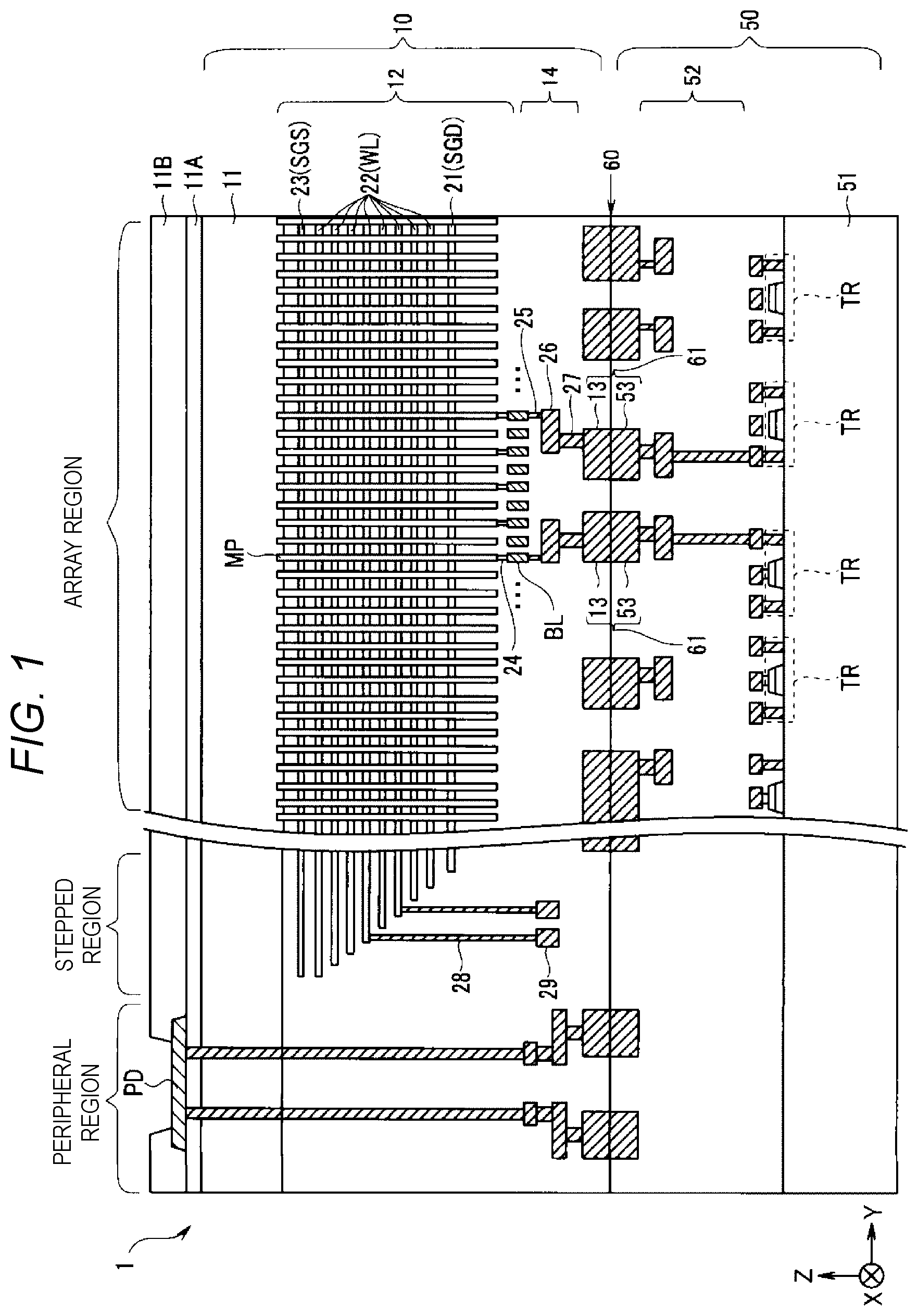
is a sectional view showing one example of a configuration of a semiconductor memory device according to a first embodiment. As shown in , a semiconductor memory device 1 has a structure wherein an array chip 10 , on which a memory cell array is formed, and a circuit chip 50 , on which a control circuit that controls the memory cell array is formed, are bonded together. The array chip 10 configures a first chip, and the circuit chip 50 configures a second chip.
The semiconductor memory device 1 is manufactured by the array chip 10 including the memory cell array being formed on a first wafer, the circuit chip 50 including the control circuit being formed on the second wafer, the first and second wafers being bonded together, and the bonded first and second wafers being diced. The semiconductor memory device 1 may also be manufactured by the array chip 10 configuring the first chip and the circuit chip 50 configuring the second chip being bonded together after the first and second wafers are individually diced.
The array chip 10 has a semiconductor substrate 11 , a memory cell array 12 including a multiple of memory cells formed on the semiconductor substrate 11 (in a −Z direction), a multiple of bonding pads 13 , and a wiring layer 14 that connects the memory cell array 12 and the bonding pads 13 .
The memory cell array 12 includes a wiring layer 21 , which is a select gate line SGD, wiring layers 22 , which are word lines WL, and a wiring layer 23 , which is a select gate line SGS. That is, the multiple of wiring layers 21 , 22 , and 23 are stacked in a Z direction (a first direction). For the sake of convenience, a structure wherein eight of the wiring layers 22 functioning as the word lines WL are stacked is shown in , but still more wiring layers may be stacked. Further, a multiple of memory holes penetrating the wiring layers 21 , 22 , and 23 and reaching the semiconductor substrate 11 are formed. A block insulating film, a charge storage layer, and a tunnel insulating film are formed sequentially on side faces of the memory holes, and furthermore, a semiconductor pillar is embedded. A memory pillar MP is configured with the semiconductor pillar, the tunnel insulating film, the charge storage layer, and the block insulating film. An insulating core may be embedded in an interior of the semiconductor pillar.
Each memory pillar MP is electrically connected via a contact plug 24 to one of a multiple of bit lines BL extending in an X direction (a second direction) intersecting the Z direction. The multiple of bit lines BL are arranged in a Y direction (a third direction) intersecting the Z direction and the X direction. Each bit line BL is electrically connected to one of the bonding pads 13 via a via plug 25 , a wiring layer 26 , and a via plug 27 . The bonding pads 13 are electrically connected to bonding pads 53 of the opposing circuit chip 50 .
The array chip 10 includes an array region, a stepped region, and a peripheral region. The memory cell array 12 is formed in the array region. The wiring layers 22 are formed in a stepped form in the stepped region. Each wiring layer 22 is electrically connected to a wiring layer 29 via a via plug 28 in the stepped region.
An insulating layer 11 A is formed on a Z-direction upper face of the semiconductor substrate 11 of the array chip 10 . A passivation film 11 B is formed on a Z-direction upper face of the insulating layer 11 A. The passivation film 11 B is an insulating film such as a silicon dioxide film. An aperture that causes an upper face of an electrode pad PD to be exposed is provided in the passivation film 11 B.
The electrode pad PD functions as an external connection pad (a bonding pad) of the semiconductor memory device 1 . The electrode pad PD is connected to a mounting substrate or other device via the aperture formed in the passivation film 11 B using bonding wire, a solder ball, a metal bump, or the like.
Various kinds of circuit for controlling the array chip 10 , that is, for controlling a writing and an erasing of data into and from the memory cells, a reading of data from the memory cells, and the like, are formed on the circuit chip 50 . For example, a logic control circuit, a sense amplifier, a row decoder, a register, a sequencer, a voltage generating circuit, and the like, are formed on the circuit chip 50 .
Also, the circuit chip 50 includes a multiple of transistors TR configuring various kinds of circuit, a wiring layer 52 , and the bonding pads 53 on a semiconductor substrate 51 . Gate electrodes, sources, and drains of the multiple of transistors TR are electrically connected to one of the bonding pads 53 via the wiring layer 52 . The bonding pads 53 are electrically connected to the bonding pads 13 of the opposing array chip 10 .
The array chip 10 and the circuit chip 50 are joined at a bonding face 60 using heat treatment. The bonding pad 13 and the bonding pad 53 are joined by the heat treatment, whereby a bonding pad 61 is formed at the bonding face 60 . As a result, multiple bonding pads 61 are provided at the bonding face 60 of the array chip 10 and the circuit chip 50 .
is a drawing illustrating a connection relationship between memory pillars and bit lines.
The memory cell array 12 is configured with a multiple of blocks BLK. An insulating layer ST shown in isolates one block BLK from another block BLK. One block BLK includes a multiple of string units SU isolated by an insulating layer SHE. The insulating layer SHE is extended as far as the wiring layer 21 configuring the select gate line SGD, thereby isolating individual string units SU from each other.
A multiple of memory pillars MP are disposed staggered in the string unit SU. Each memory pillar MP is connected to one bit line BL via the contact plug 24 .
The bit line BL connected to a memory pillar MP 1 , and the bit line BL connected to a memory pillar MP 4 neighboring the memory pillar MP 1 , are neighboring. Also, the bit line BL connected to the memory pillar MP 1 and the bit line BL connected to a memory pillar MP 2 neighboring the memory pillar MP 1 are four bit lines away from each other. When an interval between bit lines BL is within four bit lines in this way, the memory pillars MP connected to those bit lines BL are neighboring.
Meanwhile, the bit line BL connected to the memory pillar MP 1 and the bit line BL connected to a memory pillar MP 5 , which does not neighbor the memory pillar MP 1 , are five bit lines away from each other. Also, the bit line BL connected to the memory pillar MP 1 and the bit line BL connected to a memory pillar MP 3 , which does not neighbor the memory pillar MP 1 , are eight bit lines away from each other. When an interval between bit lines BL is five bit lines or greater in this way, the memory pillars MP connected to those bit lines BL are not neighboring.
is a sectional view showing a connection relationship between bonding pads and memory pillars according to a comparative example. A configuration shown in is a schematic view showing an electrical connection.
A structure shown in is such that a bonding pad 61 A formed of a bonding pad 13 A and a bonding pad 53 A, and a bonding pad 61 B formed of a bonding pad 13 B and a bonding pad 53 B, are neighboring bonding pads. Also, memory pillars MP 1 and MP 2 are neighboring memory pillars. Furthermore, memory pillars MP 2 and MP 3 are neighboring memory pillars. Meanwhile, the memory pillars MP 1 and MP 3 are non-neighboring memory pillars.
The configuration of the comparative example is such that the bonding pad 61 A is connected to a bit line BL 1 via a via plug 27 A, a wiring layer 26 A, and a via plug 25 A. The bit line BL 1 is connected to the memory pillar MP 1 via a contact plug 24 A.
Also, the bonding pad 61 B neighboring the bonding pad 61 A is connected to a bit line BL 5 four bit lines away from the bit line BL 1 via a via plug 27 B, a wiring layer 26 B, and a via plug 25 B. The bit line BL 5 is connected to the memory pillar MP 2 via a contact plug 24 B.
As described above, when an interval between bit lines BL (the number of bit lines away from each other) is within four bit lines, the memory pillars MP connected to those bit lines BL are neighboring. That is, in the case of the configuration of the comparative example, the neighboring bonding pads 61 A and 61 B are connected to the neighboring memory pillars MP 1 and MP 2 , respectively. When a short circuit failure occurs when evaluating electrical characteristics, the configuration of the comparative example is such that it cannot be determined whether the short circuit failure occurred between the neighboring bonding pads 61 A and 61 B or between the neighboring memory pillars MP 1 and MP 2 .
is a sectional view showing a connection relationship between bonding pads and memory pillars according to the first embodiment. A configuration shown in is a schematic view showing an electrical connection. Also, in , identical reference signs are allotted to configurations which are the same as those in , and a description thereof will be omitted.
As shown in , a configuration of at least one embodiment is such that the bonding pad 61 B neighboring the bonding pad 61 A is connected to a bit line BL 9 , which is eight bit lines away from the bit line BL 1 , via a via plug 27 C, a wiring layer 26 C, and a via plug 25 C. More specifically, the multiple of bit lines BL have the bit line BL 1 , which connects the memory pillar MP 1 to the bonding pad 61 A, and the bit line BL 9 , which connects the memory pillar MP 3 to the bonding pad 61 B. Further, seven or more of the multiple of bit lines BL are arranged between the bit lines BL 1 and BL 9 in the Y direction. As described above, when an interval between bit lines BL is five bit lines or greater, the memory pillars MP connected to those bit lines BL are not neighboring. This means that due to the bit lines BL 1 and BL 9 , wherein the interval between the bit lines is five bit lines or greater, being connected to the neighboring bonding pads 61 A and 61 B, the neighboring bonding pads 61 A and 61 B are connected to the non-neighboring memory pillars MP 1 and MP 3 , respectively.
This kind of configuration of at least one embodiment is such that when a short circuit failure occurs when evaluating electrical characteristics, it can be determined whether the short circuit failure occurred between the neighboring memory pillars MP 1 and MP 2 or between the neighboring bonding pads 61 A and 61 B. For example, when a failure occurs in electrical characteristics between the bonding pads 61 A and 61 B, it can be determined that the failure is a short circuit failure between the bonding pads 61 A and 61 B because the memory pillars MP 1 and MP 3 connected to the bonding pads 61 A and 61 B are not neighboring.
is a perspective view showing one example of a connection relationship between bonding pads and bit lines according to the first embodiment. is a top view showing one example of a connection relationship between bonding pads and bit lines according to the first embodiment.
As shown in , the bonding pad 61 A is connected to the bit line BL 1 via the via plug 27 A, the wiring layer 26 A, and the via plug 25 A.
The bonding pad 61 B neighboring the bonding pad 61 A is disposed moved in the Y direction (the third direction) with respect to the bonding pad 61 A. Because of this, the bonding pad 61 B is connected to the bit line BL 9 , which is eight bit lines away from the bit line BL 1 , via the via plug 27 C, the wiring layer 26 C, and the via plug 25 C.
A bonding pad 61 C is neighboring the bonding pad 61 B. The bonding pad 61 C neighboring the bonding pad 61 B is disposed moved in a −Y direction (a fourth direction) with respect to the bonding pad 61 B. Because of this, the bonding pad 61 C is connected to a bit line BL 0 , which is nine bit lines away from the bit line BL 9 , via a via plug 27 D, a wiring layer 26 D, and a via plug 25 D.
Although omitted from the drawings, the bonding pad 61 neighboring the bonding pad 61 C is disposed moved in the Y direction with respect to the bonding pad 61 C, and is connected to a bit line BL 8 that is nine bit lines away from the bit line BL 0 .
In this way, neighboring bonding pads 61 are connected to bit lines BL leaving an interval of eight bit lines or greater. As a result of this, the neighboring bonding pads 61 are connected to non-neighboring memory pillars MP, because of which distinguishing between a short circuit failure between the bonding pads 61 and a short circuit failure between the memory pillars MP is easy.
Connection of the bonding pads 61 and the bit lines BL is not limited to the connection relationship shown in . is a top view showing one example of a connection relationship between bonding pads and bit lines according to a first modification of the first embodiment. is a top view showing one example of a connection relationship between bonding pads and bit lines according to a second modification of the first embodiment.
First Modification
As shown in , the bonding pad 61 A is connected to the bit line BL 1 via the via plug 27 A, the wiring layer 26 A, and the via plug 25 A.
The bonding pad 61 B neighboring the bonding pad 61 A is disposed moved in the Y direction with respect to the bonding pad 61 A. Because of this, the bonding pad 61 B is connected to the bit line BL 9 , which is eight bit lines away from the bit line BL 1 , via the via plug 27 C, the wiring layer 26 C, and the via plug 25 C.
The bonding pad 61 C neighboring the bonding pad 61 B is disposed in the Y direction with respect to the bonding pad 61 B. Because of this, the bonding pad 61 C is connected to a bit line BL 17 , which is eight bit lines away from the bit line BL 9 , via the via plug 27 D, the wiring layer 26 D, and the via plug 25 D.
For example, eight bonding pads 61 are assumed to be one set. Further, the bonding pad 61 nine bonding pads away from the bonding pad 61 A is connected to the bit line BL 0 . Subsequently, the neighboring bonding pad 61 is connected to the bit line BL eight bit lines away from the bit line BL 0 .
According to the configuration of the first modification, neighboring bonding pads 61 are connected to non-neighboring memory pillars MP, because of which distinguishing between a short circuit failure between the bonding pads 61 and a short circuit failure between the memory pillars MP is easier.
Second Modification
A configuration shown in is such that an interval between bit lines BL to be connected is eight bit lines or greater owing to positions of the via plugs 25 A, 25 C, and 25 D being shifted, without shifting positions of the bonding pads 61 A, 61 B, and 61 C.
The via plug 25 A is disposed in a first position on the wiring layer 26 A. Because of this, the bonding pad 61 A is connected to the bit line BL 1 . The configuration of is such that although a position of the bit line BL 1 is changed from that in the configuration of , the bit line connected to the via plug 25 A is assumed to be the bit line BL 1 in , and the bit lines disposed to the right side from the bit line BL 1 are assumed to be the bit lines BL 2 , BL 3 , and so on, in order.
The via plug 25 C is disposed in a second position on the wiring layer 26 C. The second position is a position shifted in the Y direction with respect to the first position in order that connection is made to a bit line BL 10 , which is nine bit lines away from the bit line BL 1 . Because of this, the bonding pad 61 B neighboring the bonding pad 61 A is connected to the bit line BL 10 , which is nine bit lines away from the bit line BL 1 , via the via plug 27 C, the wiring layer 26 C, and the via plug 25 C.
The via plug 25 D is disposed in a third position on the wiring layer 26 D. The third position is a position shifted in the −Y direction with respect to the second position in order that connection is made to the bit line BL 2 , which is eight bit lines away from the bit line BL 10 . Because of this, the bonding pad 61 C neighboring the bonding pad 61 B is connected to the bit line BL 2 , which is eight bit lines away from the bit line BL 10 , via the via plug 27 D, the wiring layer 26 D, and the via plug 25 D.
For example, sixteen bonding pads 61 are assumed to be one set, and the via plug 25 is shifted. Further, disposition positions are shifted in the Y direction every sixteen bonding pads 61 , and connection is made to the bit lines BL.
According to the configuration of the second modification, neighboring bonding pads 61 are connected to non-neighboring memory pillars MP, because of which distinguishing between a short circuit failure between the bonding pads 61 and a short circuit failure between the memory pillars MP is easier.
Second Embodiment
Next, a second embodiment will be described.
In the first embodiment, a configuration wherein neighboring bonding pads 61 are connected to non-neighboring memory pillars MP is described. In the second embodiment, a configuration wherein non-neighboring bonding pads 61 are connected to neighboring memory pillars MP will be described.
is a sectional view showing a connection relationship between bonding pads and memory pillars according to the second embodiment. In , identical reference signs are allotted to configurations the same as those in , and a description thereof will be omitted.
As shown in , the bonding pad 61 A is formed of the bonding pads 13 A and 53 A, the bonding pad 61 B is formed of the bonding pads 13 B and 53 B, and the bonding pad 61 C is formed of bonding pads 13 C and 53 C, at the bonding face 60 .
The bonding pads 61 A and 61 B are neighboring bonding pads. Also, the bonding pads 61 B and 61 C are neighboring bonding pads. The bonding pads 61 A and 61 C are non-neighboring bonding pads.
The configuration of at least one embodiment is such that the bonding pad 61 C, which is not neighboring the bonding pad 61 A, is connected via the via plug 27 D, the wiring layer 26 D, and the via plug 25 D to the bit line BL 5 , which is four bit lines away from the bit line BL 1 . As heretofore described, when an interval between bit lines BL is within four bit lines, the memory pillars MP connected to those bit lines BL are neighboring. This means that owing to the bit lines BL 1 and BL 5 , wherein the interval between the bit lines BL is within four bit lines, being connected to the non-neighboring bonding pads 61 A and 61 C, the non-neighboring bonding pads 61 A and 61 C are connected to the neighboring memory pillars MP 1 and MP 2 , respectively.
This configuration of at least one embodiment is such that when a short circuit failure occurs when evaluating electrical characteristics, it can be determined whether the short circuit failure occurred between the neighboring memory pillars MP 1 and MP 2 or between the neighboring bonding pads 61 A and 61 B. For example, when a failure occurs in electrical characteristics between the non-neighboring bonding pads 61 A and 61 C, it can be determined that the failure is a short circuit failure between the neighboring memory pillars MP 1 and MP 2 connected to the bonding pads 61 A and 61 C.
While certain embodiments have been described, these embodiments have been presented by way of example only, and are not intended to limit the scope of the disclosure. Indeed, the novel embodiments described herein may be embodied in a variety of other forms; furthermore, various omissions, substitutions and changes in the form of the embodiments described herein may be made without departing from the spirit of the disclosure. The accompanying claims and their equivalents are intended to cover such forms or modifications as would fall within the scope and spirit of the disclosure.
Figures (9)
Citations
This patent cites (7)
- US10354987
- US2016/0079164
- US2019/0287955
- US2020/0395341
- US2021/0320114
- US2022/0310613
- US6203152