Abstract
A display device according to the present disclosure includes an optical member, a first electro-optical member, a housing, and an adhesive layer. The optical member has translucency and has a back surface including a first region and a second region outside the first region. The first electro-optical member is disposed on a back surface side of the optical member, has an optical characteristic changed with voltage application, and has a back surface including a third region and a fourth region outside the third region. The housing is disposed on the back surface side of the optical member and outside the first electro-optical member, and has a protruding portion extending along the back surface of the first electro-optical member. The adhesive layer is disposed between the third region and the protruding portion.
Claims (12)
1. A display device comprising: an optical member that has translucency and has a back surface including a first region and a second region outside the first region; a first electro-optical member that is disposed on the back surface side of the optical member, has an optical characteristic changed with voltage application, and has a back surface including a third region and a fourth region outside the third region; a housing that is disposed on the back surface side of the optical member and outside the first electro-optical member, and has a protruding portion extending along the back surface of the first electro-optical member; an adhesive layer that is disposed between the fourth region and the protruding portion in a direction perpendicular to a front surface of the optical member; a half mirror film that covers the third region; and a light shielding frame that covers the second region, wherein when viewed from the direction perpendicular to the front surface of the optical member, the light shielding frame and the half mirror film have an overlapping portion that is stripe-shaped and a width of the overlapping portion is 0.5 mm or less, and the first electro-optical member is provided between the light shielding frame and the half mirror film in the direction perpendicular to the front surface of the optical member.
7. A display device comprising: an optical member that has translucency and has a back surface including a first region and a second region outside the first region; a first electro-optical member that is disposed on the back surface side of the optical member, has an optical characteristic changed with voltage application, and has a back surface including a third region and a fourth region outside the third region; a housing that is disposed on the back surface side of the optical member and outside the first electro-optical member; a half mirror film that covers the third region; and a light shielding frame that covers the second region, wherein when viewed from a direction perpendicular to a front surface of the optical member, the light shielding frame and the half mirror film have an overlapping portion that is stripe-shaped and a width of the overlapping portion is 0.5 mm or less, and the first electro-optical member is provided between the light shielding frame and the half mirror film in the direction perpendicular to the front surface of the optical member.
10. A display device comprising: an optical member that has translucency and has a back surface including a first region and a second region outside the first region; a first electro-optical member that is disposed on the back surface side of the optical member, has an optical characteristic changed with voltage application, and has a back surface including a third region and a fourth region outside the third region; a housing that is disposed on the back surface side of the optical member and outside the first electro-optical member; a half mirror film that covers the third region; and a light shielding frame that covers the second region, wherein when viewed from a direction perpendicular to a front surface of the optical member, the light shielding frame and the half mirror film have an overlapping portion that is stripe-shaped where the overlapping portion has a width that is 0.5 mm or less.
Show 9 dependent claims
2. The display device according to claim 1 , further comprising a second electro-optical member that is disposed on the back surface side of the first electro-optical member and has an optical characteristic that is changeable with voltage application.
3. The display device according to claim 1 , wherein the half mirror film covers the first region and the second region, the half mirror film has a back surface including a fifth region and a sixth region outside the fifth region, and the light shielding frame covers the sixth region.
4. The display device according to claim 1 , wherein the housing has a side wall portion that covers an end surface of the first electro-optical member externally, outside the first electro-optical member, and the protruding portion protrudes from the side wall portion in a direction along the back surface of the first electro-optical member.
5. The display device according to claim 1 , wherein the light shielding frame is a mirror-finished printing formed by applying a resin containing a silver pigment.
6. The display device according to claim 1 , wherein the light shielding frame is a frame-shaped sheet of a resin containing a silver pigment.
8. The display device according to claim 7 , wherein the light shielding frame is a mirror-finished printing formed by applying a resin containing a silver pigment.
9. The display device according to claim 7 , wherein the light shielding frame is a frame-shaped sheet of a resin containing a silver pigment.
11. The display device according to claim 10 , wherein the light shielding frame is a mirror-finished printing formed by applying a resin containing a silver pigment.
12. The display device according to claim 10 , wherein the light shielding frame is a frame-shaped sheet of a resin containing a silver pigment.
Full Description
Show full text →
CROSS-REFERENCE TO RELATED APPLICATIONS
This application is based upon and claims the benefit of priority from Japanese Patent Application No. 2022-057057, filed on Mar. 30, 2022, the entire contents of which are incorporated herein by reference.
FIELD
The present disclosure relates to a display device.
BACKGROUND
A display device such as an electronic mirror has a display region inside a frame region on a front surface. The display device displays an image in the display region on the front surface in a display mode, and causes the display region on the front surface to function as a mirror in a mirror mode.
A conventional technique is disclosed in U.S. Ser. No. 10/850,667 B2.
In a display device, from a viewpoint of miniaturization and/or weight reduction, frame narrowing in which a width of a frame region is narrowed is desired.
The present disclosure provides a display device in which a frame can be narrowed.
SUMMARY
A display device according to the present disclosure includes an optical member, a first electro-optical member, a housing, and an adhesive layer. The optical member has translucency and has a back surface including a first region and a second region outside the first region. The first electro-optical member is disposed on a back surface side of the optical member, has an optical characteristic changed with voltage application, and has a back surface including a third region and a fourth region outside the third region. The housing is disposed on the back surface side of the optical member and outside the first electro-optical member, and has a protruding portion extending along the back surface of the first electro-optical member. The adhesive layer is disposed between the third region and the protruding portion.
BRIEF DESCRIPTION OF THE DRAWINGS
is a diagram illustrating a vehicle on which an electronic mirror system including a display device according to an embodiment is mounted;
is a front diagram illustrating a configuration of the display device according to the embodiment;
is a cross-sectional diagram illustrating a configuration of the display device according to the embodiment;
A and 4 B are cross-sectional diagrams illustrating frame narrowing in the embodiment;
is a cross-sectional diagram illustrating a reason for generation of a black line in the embodiment;
A and 6 B are cross-sectional diagrams illustrating a change in a black line width (in a case where a width of an overlapping portion is OV 1 ) according to an angle in oblique view in the embodiment;
is a graph illustrating a change in a black line width (in a case where a width of an overlapping portion is OV 1 ) according to an angle in oblique view in the embodiment;
A and 8 B are cross-sectional diagrams illustrating a change in black line width (in a case where a width of an overlapping portion is OV 2 (>OV 1 )) according to an angle in oblique view in the embodiment;
is a graph illustrating a change in a black line width (in a case where a width of an overlapping portion is OV 2 (>OV 1 )) according to an angle in oblique view in the embodiment;
A and 10 B are cross-sectional diagrams illustrating a change in black line width (in a case where a width of an overlapping portion is OV 3 (>OV 2 )) according to an angle in oblique view in the embodiment;
is a graph illustrating a change in a black line width (in a case where a width of an overlapping portion is OV 3 (>OV 2 )) according to an angle in oblique view in the embodiment; and
is a cross-sectional diagram illustrating a configuration of a display device according to a modification example of the embodiment.
DETAILED DESCRIPTION
Hereinafter, an embodiment of a display device according to the present disclosure will be described with reference to the drawings.
Embodiment
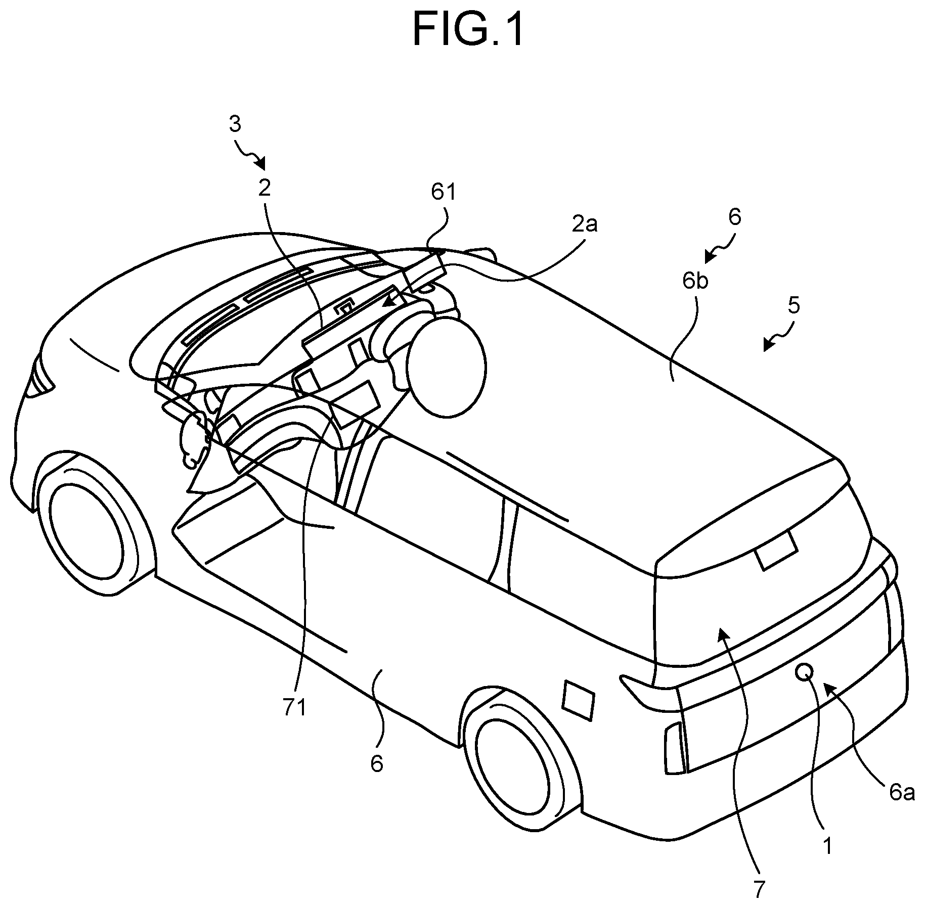
The display device according to the embodiment is, for example, an electronic mirror. The display device according to the embodiment has a frame region at an edge portion on a front surface, but is devised to have a narrowed width of the frame region. Narrowing the width of the frame region may be referred to as frame narrowing. For example, an electronic mirror system 3 can be mounted on a vehicle 5 as illustrated in . is a diagram illustrating the vehicle 5 on which the electronic mirror system 3 is mounted. The electronic mirror system 3 includes an imaging device 1 and a display device 2 .
The imaging device 1 is an onboard camera mounted on the vehicle 5 , and is installed outside or inside a vehicle body 6 . The imaging device 1 may be installed at a rear end portion of the vehicle body 6 and applied to a rear electronic mirror, may be installed at an end portion near a door of the vehicle body 6 and applied to a side electronic mirror, or may be installed at a front end portion of the vehicle body 6 and applied to a front electronic mirror.
The display device 2 is disposed in a vehicle interior 7 . The display device 2 is, for example, an electronic mirror, has a front surface 2 a , and can display an image acquired by the imaging device 1 on the front surface 2 a . The display device 2 is configured to be switchable between a display mode and a mirror mode. The display mode is a mode in which the display device 2 functions as a display that displays an image captured by the imaging device 1 . The mirror mode is a mode in which the display device 2 functions as a mirror.
In a case where the display device 2 is an electronic mirror for rear visual recognition, the display device 2 may be mounted in the form of a rearview mirror, and may have a shape in which the front surface 2 a faces a vehicle interior 7 and a shape of the front surface 2 a is a mirror surface of the rearview mirror. In a case where the display device 2 is an electronic mirror for side visual recognition, the display device 2 may be mounted in the form of a side-view mirror (for example, a side-view mirror 61 ), and may have a shape in which the front surface 2 a faces the rear of the vehicle body 6 and a shape of the front surface 2 a is a mirror surface of the side-view mirror. In a case where the display device 2 is an electronic mirror for forward recognition, the display device 2 may be mounted in the form of a vehicle-mounted display device (for example, a display device 71 ), and may have a shape in which the front surface 2 a faces the vehicle interior 7 and the shape of the front surface 2 a is a display unit of the display device.
illustrates a configuration in which the imaging device 1 is installed at an end portion 6 a on a rear side of the vehicle body 6 , and the display device 2 is applied to an electronic mirror for rear visual recognition. The electronic mirror for rear visual recognition is also called an electronic rearview mirror. The imaging device 1 acquires an image of a rear side of the vehicle body. The display device 2 can display an image of the rear side of the vehicle body captured by the imaging device 1 .
The display device 2 is as illustrated in when viewed from a front surface 2 a side. is a front diagram illustrating a configuration of the display device 2 . Hereinafter, a direction perpendicular to the front surface 2 a is defined as a Z direction, and two directions orthogonal to each other in the front surface 2 a are defined as an X direction and a Y direction.
The front surface 2 a has, for example, a rectangular shape with rounded corners in an XY plane view. The front surface 2 a has a frame region 2 a 1 and a display region 2 a 2 . The frame region 2 a 1 is a portion serving as an edge on the front surface 2 a . The display region 2 a 2 is a portion inside the frame region 2 a 1 on the front surface 2 a.
The display device 2 displays an image in the display region 2 a 2 on the front surface 2 a in a display mode, and causes the display region 2 a 2 on the front surface 2 a to function as a mirror in a mirror mode.
The display device 2 may have a variable reflectance mirror (VRM) function. In the case of having the VRM function, the display device 2 may change a reflectance of the display region 2 a 2 according to luminance or the like of a reflected image in the mirror mode. For example, in the mirror mode, in a case where the luminance of the reflected image is less than a predetermined luminance, the display device 2 may maintain the reflectance of the display region 2 a 2 at RR 1 . In a case where the luminance of the reflected image is equal to or higher than a predetermined luminance, the display device 2 may decrease the reflectance of the display region 2 a 2 to RR 2 (<RR 1 ). The case where the luminance of the reflected image is equal to or higher than a predetermined luminance is a case where the headlight of a following vehicle is reflected at a predetermined luminance or higher, a case where sunlight is reflected in a rear image at a predetermined luminance or higher, or the like. Accordingly, the display device 2 can realize automatic anti-glare by the VRM in the mirror mode. In addition, the display device 2 may decrease the reflectance of the display region 2 a 2 to RR 3 (<<RR 2 ) in the display mode. Accordingly, in the display mode, the display device 2 can display an image of an electro-optical member 27 (see ) while transmitting the image through the front surface 2 a.
On the front surface 2 a , the frame region 2 a 1 generally has a width W 1 at a portion extending in the Y direction, and generally has a width W 2 at a portion extending in the X direction. The width W 1 and the width W 2 may be equal to or different from each other.
In the display device 2 , as illustrated in , the width W 1 of the frame region 2 al on the front surface 2 a can be narrowed by devising an arrangement of an adhesive layer 24 . is an XZ cross-sectional diagram illustrating the configuration of the display device 2 , and illustrates an XZ cross section along line A-A in . In , a structure of the XZ cross section corresponding to the portion of the frame region 2 al extending in the Y direction is illustrated, but an aspect of the present embodiment is similarly applicable to a structure of the YZ cross section corresponding to the portion of the frame region 2 al extending in the X direction.
For example, as illustrated in , the display device 2 includes an optical member 21 , an electro-optical member 22 , a housing 23 , an adhesive layer 24 , a half mirror film 25 , a light shielding frame 26 , an electro-optical member 27 , an adhesive layer 28 , a frame member 29 , a frame member 30 , an optical member 31 , and a case 32 . The VRM function is mainly realized by the electro-optical member 22 and the half mirror film 25 .
The optical member 21 extends in a plate shape in an XY direction and has a substantially rectangular shape whose longitudinal direction is the X direction. The optical member 21 has translucency. The optical member 21 may be formed of inorganic glass containing SiO 2 , or may be formed of organic glass containing a transparent resin such as polymethyl methacrylate (PMMA) resin or polycarbonate (PC). The optical member 21 is also called a cover panel, and can protect the display device 2 from an external impact or the like.
The optical member 21 has a front surface 2 a on a +Z side and a back surface 21 a on a −Z side. The front surface 2 a has a frame region 2 a 1 and a display region 2 a 2 . The frame region 2 a 1 is an edge portion of the front surface 2 a , and extends in a stripe shape in the Y direction or the X direction along an outer contour of the front surface 2 a (see ). The display region 2 a 2 extends planarly in the XY direction inside the frame region 2 a 1 . The back surface 21 a has a region 21 a 1 and a region 21 a 2 . The region 21 a 2 is located outside the region 21 a 1 in the XY direction. The region 21 a 2 corresponds to the frame region 2 a 1 , and overlaps the frame region 2 a 1 when viewed from the Z direction. The region 21 a 1 corresponds to the display region 2 a 2 and overlaps the display region 2 a 2 when viewed from the Z direction.
The light shielding frame 26 is disposed between the optical member 21 and the electro-optical member 22 in the Z direction. The light shielding frame 26 is disposed between the region 21 a 2 and the electro-optical member 22 in the Z direction. The light shielding frame 26 has a substantially rectangular outer contour whose longitudinal direction is the X direction. The light shielding frame 26 has an opening corresponding to the display region 2 a 2 . The light shielding frame 26 is in contact with the back surface 21 a of the optical member 21 on the +Z side, and covers the region 21 a 2 . The light shielding frame 26 is in contact with the electro-optical member 22 on the −Z side, and covers a +Z side surface of the electro-optical member 22 .
A color of the light shielding frame 26 desirably corresponds to a color of the display region 2 a 2 when the front surface 2 a is observed from the +Z side. When the color of the display region 2 a 2 is silver, the light shielding frame 26 may be mirror-finished printing formed by applying a resin containing a silver pigment to the region 21 a 2 of the back surface 21 a of the optical member 21 , or may be a frame-shaped sheet of a resin containing a silver pigment attached to the region 21 a 2 of the back surface 21 a of the optical member 21 . When the color of the display region 2 a 2 is silver close to black, the light shielding frame 26 may be black printing formed by applying a resin containing a black pigment to the region 21 a 2 of the back surface 21 a of the optical member 21 , or may be a frame-shaped sheet of a resin containing a black pigment attached to the region 21 a 2 of the back surface 21 a of the optical member 21 .
The electro-optical member 22 is disposed on the back surface side (−Z side) of the optical member 21 . The electro-optical member 22 is disposed on the back surface side (−Z side) of the light shielding frame 26 . The electro-optical member 22 has an optical characteristic thereof which can be changed with voltage application. The electro-optical member 22 has a liquid crystal region 221 and a peripheral region 222 . A boundary between the liquid crystal region 221 and the peripheral region 222 in the electro-optical member 22 defines a boundary between the display region 2 a 2 and the frame region 2 a 1 on the front surface 2 a . The peripheral region 222 may be bonded to the back surface of the light shielding frame 26 with a transparent adhesive such as OCA.
The electro-optical member 22 has a front surface 22 b on the +Z side and a back surface 22 a on the −Z side. The front surface 22 b has a region 22 b 1 and a region 22 b 2 . The region 22 b 2 is located outside the region 22 b 1 in the XY direction. The region 22 b 2 corresponds to the frame region 2 a 1 , and overlaps the frame region 2 a 1 when viewed from the Z direction. The region 22 b 1 corresponds to the display region 2 a 2 and overlaps the display region 2 a 2 when viewed from the Z direction. The back surface 22 a has a region 22 a 1 and a region 22 a 2 . The region 22 a 2 is located outside the region 22 a 1 in the XY direction. The region 22 a 2 corresponds to the frame region 2 a 1 , and overlaps the frame region 2 a 1 when viewed from the Z direction. The region 22 a 1 corresponds to the display region 2 a 2 and overlaps the display region 2 a 2 when viewed from the Z direction.
The light shielding frame 26 covers the region 22 b 2 . The region 22 b 2 corresponds to the peripheral region 222 of the electro-optical member 22 . As a result, elements, wirings, terminals, and the like disposed in the peripheral region 222 of the electro-optical member 22 can be shielded, and an appearance of the display device 2 can be improved.
The liquid crystal region 221 corresponds to the display region 2 a 2 and extends in the XY direction. The liquid crystal region 221 includes, for example, a TN type liquid crystal panel 221 a and a polarizing plate 221 b disposed on the +Z side thereof. The liquid crystal panel 221 a has a configuration in which a TN type liquid crystal material is sealed between a pair of transparent substrates disposed apart from each other in the Z direction and extending in the XY direction. The peripheral region 222 corresponds to the frame region 2 a 1 and extends so as to surround the periphery of the liquid crystal region 221 in the XY planar view. In the peripheral region 222 , end portions of a pair of transparent substrates are disposed, and a member for sealing the liquid crystal material is disposed. Of the pair of transparent substrates, a +Z side surface of an end portion of the transparent substrate on the +Z side may be bonded to the back surface of the light shielding frame 26 with a transparent adhesive such as OCA. A −Z side surface of the end portion of the transparent substrate on the −Z side may be bonded to the housing 23 with a transparent adhesive such as OCA. A transparent electrode formed of a transparent conductive material such as ITO can be disposed on each of the pair of transparent substrates.
Also, a control circuit or the like connected to the pair of transparent electrodes may be disposed in the peripheral region 222 . The control circuit can change an alignment state of the liquid crystal molecules by changing a voltage applied to the pair of transparent electrodes, thereby changing the optical characteristic (for example, transmittance or reflectance) of the electro-optical member 22 . The VRM function is mainly realized by a change in the optical characteristic of the electro-optical member 22 and an operation of light reflection or transmission by the half mirror film 25 according to the change.
The housing 23 is disposed on the back surface side (−Z side) of the optical member 21 and is disposed outside the electro-optical member 22 in the XY direction. The housing 23 has a protruding portion 231 and a side wall portion 232 . The side wall portion 232 covers an XY direction end surface 22 c of the electro-optical member 22 externally in the XY direction, outside the electro-optical member 22 in the XY direction. The side wall portion 232 extends in the YZ direction or the ZX direction (see ) and forms an outer surface 23 a of the housing 23 . The protruding portion 231 protrudes from the side wall portion 232 in a direction along the back surface 22 a of the electro-optical member 22 . The protruding portion 231 extends along the back surface 22 a of the electro-optical member 22 . The housing 23 can be formed of a material having a light shielding property.
The adhesive layer 24 is disposed between the back surface 22 a of the electro-optical member 22 and the protruding portion 231 . The adhesive layer 24 may be a member such as a double-sided tape in which an adhesive is applied to a +Z side surface and a −Z side surface. The back surface 22 a of the electro-optical member 22 has the region 22 a 1 and the region 22 a 2 . The region 22 a 2 is disposed outside the region 22 a 1 in the X direction. The adhesive layer 24 is disposed between the region 22 a 2 and the protruding portion 231 , and bonds the peripheral region 222 of the electro-optical member 22 to the protruding portion 231 .
That is, the light shielding frame 26 is printed or bonded to the back surface 21 a of the optical member 21 , and bonded to the peripheral region 222 of the electro-optical member 22 via a transparent adhesive such as OCA. The adhesive layer 24 bonds the back surface 22 a of the electro-optical member 22 to the housing 23 . As a result, the optical member 21 is fixed to the housing 23 via the light shielding frame 26 and the electro-optical member 22 . As a result, a width of the adhesive layer 24 in the X direction can be secured according to a width of the peripheral region 222 in the X direction, and a bonding area of the adhesive layer 24 can be secured wide, so that an adhesive strength (for example, vibration resistance robustness) can be easily secured.
For example, as illustrated in B , in a case where an adhesive layer 24 i bonds a light shielding frame 26 i to a housing 23 i , a thickness of the housing 23 i in the X direction is increased in order to secure the width of the adhesive layer 24 i in the X direction and secure the bonding area. The adhesive layer 24 i bonds the light shielding frame 26 i to a +Z side end surface of the housing 23 i . Accordingly, an X-direction end portion 22 ci of an electro-optical member 22 i is retracted inward in the X direction, and the boundary between a liquid crystal region 221 i and a peripheral region 222 i in the electro-optical member 22 i is retracted inward in the X direction. As a result, the boundary between a display region 2 a 2 i and a frame region 2 a 1 i on a front surface 2 ai is retracted inward in the X direction, and a width W 1 i of the frame region 2 a 1 i is increased.
On the other hand, in the structure illustrated in , as illustrated in A , the adhesive layer 24 is disposed between the back surface 22 a of the electro-optical member 22 and the protruding portion 231 , and the optical member 21 is fixed to the housing 23 via the light shielding frame 26 and the electro-optical member 22 . Accordingly, the width of the adhesive layer 24 in the X direction can be secured according to the width of the peripheral region 222 in the X direction while locating the end portion 22 c of the electro-optical member 22 in the X direction further outside in the X direction. That is, the end portion 22 c of the electro-optical member 22 in the X-direction can be brought close to the outer surface 23 a of the housing 23 . Accordingly, the boundary between the liquid crystal region 221 and the peripheral region 222 in the electro-optical member 22 can be located further outside in the X direction. As a result, the boundary between the display region 2 a 2 and the frame region 2 a 1 on the front surface 2 a can be located further outside in the X direction, and the width W 1 of the frame region 2 a 1 i can be narrowed (frame narrowing).
The half mirror film 25 illustrated in is disposed between the electro-optical member 22 and the electro-optical member 27 in the Z direction. The light shielding frame 26 is disposed between the region 22 a 1 and the electro-optical member 27 in the Z direction. The half mirror film 25 has a substantially rectangular shape whose longitudinal direction is the X direction corresponding to the display region 2 a 2 (see ). The half mirror film 25 is in contact with the back surface 22 a of the electro-optical member 22 on the +Z side and covers the region 22 a 1 . The half mirror film 25 may be bonded to the back surface 22 a of the electro-optical member 22 with a transparent adhesive such as OCA. The half mirror film 25 is separated from the electro-optical member 27 on the −Z side.
For example, the display device 2 is configured such that the color of the frame region 2 a 1 and the color of the display region 2 a 2 when observed from the +Z side in the mirror mode correspond to each other. The color of the frame region 2 a 1 is formed by the color of the light shielding frame 26 , and the color of the display region 2 a 2 is mainly formed by the color of the half mirror film 25 . In this case, as indicated by a dotted line in , a black line may be visually recognized in the vicinity of the boundary between the frame region 2 a 1 and the display region 2 a 2 . It is considered that the black line is generated by light reflected on the front surface of the half mirror film 25 and directed toward the back surface of the light shielding frame 26 being shielded by the light shielding frame 26 among the light incident from the +Z side of the front surface 2 a and viewed as a shadow of the light shielding frame 26 as indicated by a one-dot chain line in . The width of the visible black line can be, for example, approximately twice the width of the light-shielded region. When the light-shielded region becomes large, the black line is easily conspicuous.
On the other hand, in the structure illustrated in , the light shielding frame 26 and the half mirror film 25 are configured to be adjacent to each other or have a stripe-shaped overlapping portion when viewed from the Z direction. In this case, as illustrated in A to 11 , the light shielding frame 26 and the half mirror film 25 are configured such that the width of the overlapping portion when viewed from the Z direction is 0.5 mm or less. As a result, the black line width can be suppressed, and the black line can be made inconspicuous.
In a case where the light shielding frame 26 and the half mirror film 25 are adjacent to each other when viewed from the Z direction, that is, in a case of “Width OV 1 of overlapping portion≈0 mm”, the black line width changes as illustrated in A and 6 B according to the angle in oblique view. The angle in oblique view is defined as an inclination angle of a line of sight of an observer with respect to a normal direction (Z direction) of the front surface 2 a . A and 6 B are cross-sectional diagrams illustrating a change in a black line width (in a case of “width of overlapping portion≈0 mm”) according to the angle in oblique view.
As illustrated in A , in a case where the angle in oblique view is θ 11 , the black line width is 2×W 11 . As illustrated in B , when the angle in oblique view increases to θ 12 (>θ 11 ), the black line width increases to 2×W 12 (>2×W 11 ) accordingly.
When the description is graphed, it is indicated by a one-dot chain line in . is a graph illustrating a change in a black line width (in a case of “width of overlapping portion≈0 mm”) according to the angle in oblique view. In , a horizontal axis represents the angle in oblique view, and a vertical axis represents the black line width. It can be seen that the black line width linearly changes according to the angle in oblique view.
On the other hand, in a case where the width of the overlapping portion between the light shielding frame 26 i and a half mirror film 25 i when viewed from the Z direction is relatively large OV 100 (>>0.5 mm) (see B ), the black line width linearly changes at a steeper inclination according to the angle in oblique view, as indicated by a dotted line in . When the maximum angle assumed when the front surface 2 a is obliquely viewed is referred to as an angle threshold θth, the black line width at the angle threshold θth is 2×W 100 in the case of the dotted line of . In the case of the one-dot chain line in , the black line width at the angle threshold θth is 2×W 10 , and an improvement amount of the black line width by setting the width OV 1 of the overlapping portion≈0 mm is ΔW 10 =2×W 100 −2×W 10 . For example, θth=34° is satisfied, and an improvement amount ΔW 10 of black line width=0.47 mm is satisfied.
In a case where a width of the overlapping portion between the light shielding frame 26 and the half mirror film 25 when viewed from the Z direction is OV 2 (>OV 1 ), the black line width changes as illustrated in A and 8 B according to the angle in oblique view. A and 8 B are cross-sectional diagrams illustrating a change in a black line width (in a case where the width of the overlapping portion is OV 2 (>OV 1 )) according to the angle in oblique view.
As illustrated in A , in a case where the angle in oblique view is θ 11 , the black line width is 2×W 21 . As compared with A , it can be seen that a shadow is easily generated due to an influence of the overlapping portion, and the black line width 2×W 21 is accordingly increased (2×W 21 >2×W 11 ). As illustrated in B , when the angle in oblique view increases to θ 22 (>θ 11 ), the black line width increases to 2×W 22 (>2×W 21 ) accordingly. The angle θ 22 of oblique view is an angle at which light passing through the +X side end of the light shielding frame 26 is incident on the −X side end of the half mirror film 25 . It is considered that when the angle in oblique view is larger than θ 22 , the influence of the overlapping portion disappears, and the black line width changes similarly to the case of width of overlapping portion≈0 mm.
When the description is graphed, it is indicated by a solid line in . is a graph illustrating a change in a black line width (in a case where the width of the overlapping portion is OV 2 (>OV 1 )) according to the angle in oblique view. In , a horizontal axis represents the angle in oblique view, and a vertical axis represents the black line width. The black line width changes at the same inclination as the dotted line until the angle in oblique view reaches θ 22 , and changes at the same inclination as the one-dot chain line when the angle in oblique view becomes θ 22 or larger. The dotted line in corresponds to the dotted line in , and indicates the change of the black line width according to the angle in oblique view in the case where the width of the overlapping portion is relatively large OV 100 . The one-dot chain line in corresponds to the one-dot chain line in , and indicates a change in the black line width according to the angle in oblique view when the width of the overlapping portion is substantially zero.
In the case of the dotted line in , the black line width at the angle threshold θth is 2×W 100 . In the case of the solid line in , the black line width at the angle threshold θth is 2×W 20 , and an improvement amount of the black line width by setting the width OV 2 of the overlapping portion is ΔW 20 =2×W 100 −2×W 20 . For example, in a case of OV 2 =0.2 mm, θ 22 =13.95° and θth=34° are satisfied, and improvement amount of black line width ΔW 20 =0.28 mm is satisfied.
In a case where the width of the overlapping portion between the light shielding frame 26 and the half mirror film 25 when viewed from the Z direction is OV 3 (>OV 2 ), the black line width changes as illustrated in A and 10 B according to the angle in oblique view. A and 10 B are cross-sectional diagrams illustrating a change in a black line width (in a case where the width of the overlapping portion is OV 3 (>OV 2 )) according to the angle in oblique view.
As illustrated in A , in a case where the angle in oblique view is θ 11 , the black line width is 2×W 31 . As compared with A , it can be seen that a shadow is easily generated due to an influence of the overlapping portion, and the black line width W 31 is accordingly increased (2×W 31 >2×W 11 ). As illustrated in B , when the angle in oblique view increases to θ 32 (>θ 11 ), the black line width increases to 2×W 32 (>2×W 31 ) accordingly. The angle θ 32 of oblique view is an angle at which light passing through the +X side end of the light shielding frame 26 is incident on the −X side end of the half mirror film 25 . It is considered that when the angle in oblique view is larger than θ 32 , the influence of the overlapping portion disappears, and the black line width changes similarly to the case of width of overlapping portion≈0 mm.
When the description is graphed, it is indicated by a solid line in . is a graph illustrating a change in a black line width (in a case where the width of the overlapping portion is OV 3 (>OV 2 )) according to the angle in oblique view. In , a horizontal axis represents the angle in oblique view, and a vertical axis represents the black line width. The black line width changes at the same inclination as the dotted line until the angle in oblique view reaches θ 32 , and changes at the same inclination as the one-dot chain line when the angle in oblique view becomes θ 32 or larger. The dotted line in corresponds to the dotted line in , and indicates the change of the black line width according to the angle in oblique view in the case where the width of the overlapping portion is relatively large OV 100 . The one-dot chain line in corresponds to the one-dot chain line in , and indicates a change in the black line width according to the angle in oblique view when the width of the overlapping portion is substantially zero.
In the case of the dotted line in , the black line width at the angle threshold θth is 2×W 100 . In the case of the solid line in , the black line width at the angle threshold θth is 2×W 30 , and an improvement amount of the black line width by setting the width OV 3 of the overlapping portion is ΔW 30 =2×W 100 −2×W 30 . For example, in a case of OV 3 =0.5 mm, 032=31.85° and θth=34° are satisfied, and improvement amount of black line width ΔW 30 =0.04 mm is satisfied. The improvement amount of the black line width is a positive value, but is close to zero.
For example, it is considered that in a case of setting the width of the overlapping portion>0.5 mm, an angle at which the inclination of the dotted line changes to the inclination of the one-dot chain line is equal to or larger than the angle threshold θth, in the change of the black line width according to the angle in oblique view. That is, it can be said that in a case of setting the width of the overlapping portion>0.5 mm, there is substantially no improvement amount of the black line width in an angle range of θth or smaller in oblique view.
On the other hand, for example, by setting 0 mm width of overlapping portion≤0.5 mm, as illustrated in , 9 , and 11 , the black line width can be suppressed and the black line can be made inconspicuous.
Returning to , the frame member 29 is disposed between the housing 23 and the electro-optical member 27 in the XY direction. The frame member 29 extends along the YZ direction or the ZX direction. The frame member 29 is bent inward in the XY direction such that an end portion on the +Z side covers the electro-optical member 27 from the +Z side. The frame member 29 may be made of a sheet-metal processable material such as metal. The frame member 29 may be fixed to the housing 23 .
The electro-optical member 27 is disposed on the back surface 22 a side (−Z side) of the electro-optical member 22 . The electro-optical member 27 is disposed between the electro-optical member 22 and the optical member 31 in the Z direction. The electro-optical member 27 is disposed between the frame member 29 and the frame member 30 in the Z direction. The electro-optical member 27 has an optical characteristic thereof which can be changed with voltage application. The electro-optical member 27 has a liquid crystal region 271 and a peripheral region 272 . The electro-optical member 27 may be, for example, a display panel for image display.
The liquid crystal region 271 corresponds to the display region 2 a 2 and extends in the XY direction. The liquid crystal region 271 includes, for example, a TFT type liquid crystal panel 271 a and a polarizing plate 271 b disposed on the +Z side thereof. The liquid crystal panel 271 a has a configuration in which a TFT type liquid crystal material is sealed between a pair of transparent substrates disposed apart from each other in the Z direction and extending in the XY direction. The peripheral region 272 corresponds to the frame region 2 a 1 and extends so as to surround the periphery of the liquid crystal region 271 in the XY planar view. In the peripheral region 272 , end portions of a pair of transparent substrates are disposed, and a member for sealing the liquid crystal material is disposed. Of the pair of transparent substrates, a −Z side surface of an end portion of the transparent substrate on the −Z side may be bonded to the frame member 30 with a transparent adhesive such as OCA. A transparent electrode formed of a transparent conductive material such as ITO can be disposed on each of the pair of transparent substrates.
Also, a control circuit or the like connected to the pair of transparent electrodes may be disposed in the peripheral region 272 . The control circuit can change an alignment state of the liquid crystal molecules by changing a voltage applied to the pair of transparent electrodes, thereby changing the optical characteristic (for example, transmittance) of the electro-optical member 27 . The image display function is mainly realized by a change in an optical characteristic of the electro-optical member 27 .
The frame member 30 is disposed between the frame member 29 and the case 32 and the optical member 31 in the XY direction. The frame member 30 extends along the YZ direction or the ZX direction. The frame member 30 has a bent portion 30 a bent inward in the XY direction such that an end portion on the +Z side covers the case 32 and the optical member 31 from the +Z side. The frame member 30 may be made of a sheet-metal processable material such as metal. The frame member 30 may be fixed to the housing 23 directly or via the frame member 29 .
The adhesive layer 28 is disposed between the back surface of the electro-optical member 27 and the bent portion 30 a of the frame member 30 . The adhesive layer 28 may be a member such as a double-sided tape in which an adhesive is applied to a +Z side surface and a −Z side surface. The adhesive layer 28 is disposed between an outer region on the back surface of the electro-optical member 27 and the bent portion 30 a of the frame member 30 , and bonds the peripheral region 272 of the electro-optical member 27 to the bent portion 30 a of the frame member 30 .
That is, the adhesive layer 28 bonds the back surface of the electro-optical member 27 to the frame member 30 . As a result, the electro-optical member 27 is fixed to the housing 23 via the frame member 30 . Accordingly, the width of the adhesive layer 28 in the X direction can be secured according to the width of the peripheral region 272 in the X direction while locating the end portion of the electro-optical member 27 in the X direction relatively outside in the X direction. As a result, a wide bonding region of the adhesive layer 28 can be secured while securing a wide display region, so that it is possible to easily secure the bonding strength.
The optical member 31 is disposed on the back surface side (−Z side) of the electro-optical member 27 . The optical member 31 extends in a plate shape in an XY direction and has a substantially rectangular shape whose longitudinal direction is the X direction. The optical member 31 is configured to illuminate the electro-optical member 27 from the back surface side. The optical member 31 is, for example, a backlight.
The case 32 is disposed on the back surface side (−Z side) of the electro-optical member 27 and is disposed on the −Z side of the optical member 31 . The case 32 has a box shape open on the +X side, and can accommodate the optical member 31 . The case 32 may be fixed to the housing 23 directly or via the frame member 30 and/or the frame member 29 .
As described above, in the embodiment, in the display device 2 , the adhesive layer 24 is disposed between the back surface 22 a of the electro-optical member 22 and the protruding portion 231 , and the optical member 21 is fixed to the housing 23 via the light shielding frame 26 , the electro-optical member 22 , and the adhesive layer 24 . That is, the end portion 22 c of the electro-optical member 22 in the X-direction can be brought close to the outer surface 23 a of the housing 23 while securing the bonding area of the adhesive layer 24 . Accordingly, the width W 1 of the frame region 2 a 1 i on the front surface 2 a can be narrowed (frame narrowing). Therefore, an attraction (design) of the appearance of the display device 2 can be improved. In addition, the display device 2 can be easily reduced in size and/or weight, the display device 2 can be reduced in cost, and adhesion by the adhesive layer 24 can be stabilized.
Also, in the embodiment, in the display device 2 , the light shielding frame 26 and the half mirror film 25 are configured to be adjacent to each other or have a stripe-shaped overlapping portion when viewed from the Z direction. For example, by setting 0 mm (width of overlapping portion when viewed from Z direction) 0.5 mm, the black line width when the front surface 2 a is observed can be suppressed, and the black line can be made inconspicuous.
Note that an aspect of the present embodiment is also applicable to a display device (for example, a half mirror type electronic mirror) having no VRM function. For example, as a modification of the embodiment, a display device 2 j can be configured as illustrated in . is a cross-sectional diagram illustrating a configuration of the display device 2 j according to a modification example of the embodiment.
The display device 2 j includes a half mirror film 25 j , a light shielding frame 26 j , and an electro-optical member 27 j instead of the half mirror film 25 , the light shielding frame 26 , and the electro-optical member 27 (see ), and the electro-optical member 22 , the frame member 29 , and the adhesive layer 28 are omitted.
The half mirror film 25 j is moved between the optical member 21 and the light shielding frame 26 with respect to the half mirror film 25 (see ), and an area thereof is enlarged so as to cover the region 21 a 1 and the region 21 a 2 of the back surface 21 a of the optical member 21 . The electro-optical member 27 j is moved between the light shielding frame 26 j and the adhesive layer 24 with respect to the electro-optical member 27 (see ).
A back surface 25 a of the half mirror film 25 j has a region 25 a 1 and a region 25 a 2 . The region 25 a 2 is located outside the region 25 a 1 in the XY direction. The region 25 a 2 corresponds to a frame region 2 a 1 j , and overlaps the frame region 2 a 1 j when viewed from the Z direction. The region 25 a 1 corresponds to a display region 2 a 2 j and overlaps the display region 2 a 2 j when viewed from the Z direction.
The light shielding frame 26 j is in contact with the back surface 25 a of the half mirror film 25 j on the +Z side and covers the region 25 a 2 . The light shielding frame 26 j is in contact with the electro-optical member 27 j on the −Z side, and covers a +Z side surface of the electro-optical member 27 j.
In the electro-optical member 27 j , the peripheral region 272 on the +Z side is bonded to the light shielding frame 26 j with an adhesive such as OCA, for example, and the peripheral region 272 on the −Z side is bonded to the protruding portion 231 of the housing 23 via the adhesive layer 24 . A function of the electro-optical member 27 j is similar to the function of the electro-optical member 27 . A back surface 27 a of the electro-optical member 27 has a region 27 a 1 and a region 27 a 2 . The region 27 a 2 is disposed outside the region 27 a 1 in the X direction.
The adhesive layer 24 is disposed between the region 27 a 2 and the protruding portion 231 , and bonds the peripheral region 272 of the electro-optical member 27 to the protruding portion 231 .
Also, in this display device 2 j , the adhesive layer 24 is disposed between the back surface 27 a of the electro-optical member 27 and the protruding portion 231 , and the optical member 21 is fixed to the housing 23 via the light shielding frame 26 j , the electro-optical member 27 , and the adhesive layer 24 . That is, the end portion 22 c of the electro-optical member 27 in the X-direction can be brought close to the outer surface 23 a of the housing 23 while securing the bonding area of the adhesive layer 24 . Accordingly, the width W 1 j of the frame region 2 a 1 j on a front surface 2 aj can be narrowed (frame narrowing).
According to the display device of the present disclosure, a frame can be narrowed.
While certain embodiments have been described, these embodiments have been presented by way of example only, and are not intended to limit the scope of the inventions. Indeed, the novel methods and systems described herein may be embodied in a variety of other forms; furthermore, various omissions, substitutions and changes in the form of the methods and systems described herein may be made without departing from the spirit of the inventions. The accompanying claims and their equivalents are intended to cover such forms or modifications as would fall within the scope and spirit of the inventions.
Figures (12)
Citations
This patent cites (13)
- US9684204
- US10850667
- US11448911
- US2009/0086123
- US2016/0278201
- US2019/0196256
- US2020/0319669
- US2022/0163838
- US2008203487
- US2009-109855
- US2014-211584
- US2022-17759
- USWO2014/112525