Abstract
A display device includes a display panel including a first non-folding area, a folding area, and a second non-folding area that are arranged in a first direction, a first support layer which is disposed below the display panel and in which a plurality of first holes overlapping the first non-folding area and the second non-folding area are defined, and a reinforcing part disposed below the first support layer. The reinforcing part includes a reinforcing layer disposed below the first support layer and a plurality of dummies extending from the reinforcing layer and disposed into the plurality of first holes.
Claims (20)
1. A display device comprising: a display panel comprising: a first non-folding area, a folding area, and a second non-folding area arranged in a first direction, and a circuit element layer and a display element layer which is disposed on the circuit element layer and connected thereto; a digitizer module disposed under the circuit element layer and the display element layer of the display panel; an electromagnetic shielding sheet disposed under the digitizer module, the electromagnetic shielding sheet being separated under the folding area; and a first support layer which is metallic and between the electromagnetic shielding sheet and the digitizer, wherein the first support layer defines a plurality of first holes in the first support layer which overlap the first non-folding area and the second non-folding area.
19. A display device comprising: a display panel comprising a first non-folding area, a folding area and a second non-folding area which are arranged in a first direction; a digitizer module under the display panel; a shielding sheet under the digitizer module, the shielding sheet separated under the folding area and comprising: a first shielding sheet which overlaps the first non-folding area and a first portion of the folding area; and a second shielding sheet which overlaps the second non-folding area and a second portion of the folding area and is spaced apart from the first shielding sheet along the first direction; a support layer which is below the display panel and in which a plurality of holes overlapping the first non-folding area and the second non-folding area are defined; and a reinforcing part below the support layer, the reinforcing part comprising: a reinforcing layer below the support layer; and a plurality of dummies extending from the reinforcing layer and into the holes.
20. An electronic apparatus comprising: a display device comprising: a first non-folding area, a folding area, and a second non-folding area arranged in a first direction, and a circuit element layer and a display element layer which is disposed on the circuit element layer and connected thereto; a digitizer module disposed under the circuit element layer and the display element layer of the display device; an electromagnetic shielding sheet disposed under the digitizer module, the electromagnetic shielding sheet being separated under the folding area; and a first support layer which is metallic and between the electromagnetic shielding sheet and the digitizer, wherein the first support layer defines a plurality of holes in the first support layer which overlap the first non-folding area and the second non-folding area.
Show 17 dependent claims
2. The display device of claim 1 , wherein the digitizer module is disposed between the display panel and the first support layer.
3. The display device of claim 1 , wherein the electromagnetic shielding sheet comprises: a first electromagnetic shielding sheet which overlaps the first non-folding area and a first portion of the folding area; and a second electromagnetic shielding sheet which overlaps the second non-folding area and a second portion of the folding area and is spaced apart from the first electromagnetic shielding sheet along the first direction.
4. The display device of claim 3 , further comprising a compensation layer which overlaps the folding area, wherein the compensation layer is disposed between the first support layer and the first electromagnetic shielding sheet and between the first support layer and the second electromagnetic shielding sheet.
5. The display device of claim 1 , further comprising a reinforcing part disposed below the first support layer, the reinforcing part comprising: a reinforcing layer which is disposed below the first support layer and entirely overlaps the first and second non-folding areas when viewed in a plan view; and a plurality of dummies extending from the reinforcing layer and into the plurality of first holes, wherein the plurality of first holes are formed by penetrating the first support layer.
6. The display device of claim 1 , wherein the plurality of first holes are arranged along the first direction and along a second direction which crosses the first direction.
7. The display device of claim 6 , further comprising a reinforcing part disposed below the first support layer, the reinforcing part comprising: a reinforcing layer which is separated under the folding area, the reinforcing layer comprising: a first reinforcing layer overlapping the first non-folding area; and a second reinforcing layer overlapping the second non-folding area and spaced apart from the first reinforcing layer along the first direction; and a plurality of dummies extending from the reinforcing layer and into the plurality of first holes.
8. The display device of claim 7 , wherein the plurality of dummies comprise: a plurality of first dummies extending from the first reinforcing layer; and a plurality of second dummies extending from the second reinforcing layer.
9. The display device of claim 1 , further comprising a reinforcing part disposed below the first support layer, the reinforcing part comprising: a reinforcing layer disposed below the first support layer; and a plurality of dummies which are nonmetallic and extend from the reinforcing layer and into the plurality of first holes.
10. The display device of claim 1 , wherein the first support layer further defines a plurality of second holes overlapping the folding area, the plurality of second holes being formed by penetrating the first support layer.
11. The display device of claim 1 , further comprising a second support layer disposed below the first support layer, wherein the second support layer comprises: a first plate overlapping the first non-folding area; and a second plate overlapping the second non-folding area and spaced apart from the first plate along the first direction.
12. The display device of claim 1 , wherein, when the folding area is folded about a folding axis extending in a second direction crossing the first direction, the display panel is in-folded so that a top surface of the first non-folding area faces a top surface of the second non-folding area.
13. The display device of claim 1 , wherein, when viewed in a plan view, the plurality of first holes have a polygonal shape.
14. The display device of claim 13 , wherein the plurality of first holes extend along the first direction.
15. The display device of claim 1 , wherein, when viewed in a plan view, the plurality of first holes have a circular shape.
16. The display device of claim 1 , further comprising: the circuit element layer and the display element layer of the display panel together defining a display layer of the display panel, and the first support layer between the electromagnetic shielding sheet and the display layer.
17. The display device of claim 1 , further comprising a reinforcing part disposed below the first support layer, the reinforcing part comprising: a reinforcing layer disposed below the first support layer; and the reinforcing layer extending from below the first support layer and into the plurality of first holes to define a plurality of dummies of the reinforcing part.
18. The display device of claim 17 , wherein the reinforcing layer defines no dummies overlapping the folding area.
Full Description
Show full text →
This application is a continuation application of U.S. patent application Ser. No. 17/220,071 filed on Apr. 1, 2021, which claims priority to Korean Patent Application No. 10-2020-0083916, filed on Jul. 8, 2020, and all the benefits accruing therefrom under 35 U.S.C. § 119, the entire contents of which are hereby incorporated by reference.
BACKGROUND
(1) Field
The disclosure herein relates to a display device, and more particularly, to a display device which is foldable and unfoldable about a folding axis.
(2) Description of the Related Art
Electronic apparatuses that provide an image to a user, such as smart phones, digital cameras, laptop computers, navigation units and smart televisions include display devices for displaying the image. Such a display device generates an image and provides the image to the user via a display screen.
With the technological development for the display device, various types of display devices have been developed. For example, various flexible display devices which may be deformable, foldable or rollable in curved shapes are being developed. The flexible display devices having diversely deformable shapes are easy to carry and improve user's convenience.
A foldable display device among the flexible display devices includes a display module that is foldable about a folding axis extending in one direction. The display module is both foldable and unfoldable about the folding axis.
SUMMARY
Embodiments of the invention provide a flexible display device including a support layer suitable to drive a digitizer module.
An embodiment provides a display device includes a display panel including a first non-folding area, a folding area, and a second non-folding area that are arranged in a first direction, a first support layer which is disposed below the display panel and in which a plurality of first holes overlapping the first non-folding area and the second non-folding area are defined, and a reinforcing part disposed below the first support layer. The reinforcing part includes a reinforcing layer disposed below the first support layer and a plurality of dummies extending from the reinforcing layer and disposed into the plurality of first holes.
In an embodiment, a display device includes a display panel including a first non-folding area, a folding area, and a second non-folding area that are arranged in a first direction, a first support layer which is disposed below the display panel, and in which a first hole overlapping each of the first and second non-folding areas and a second hole overlapping the folding area are defined, and a plurality of dummies disposed in the first hole.
In an embodiment, a display device includes a display panel which is foldable, a digitizer module disposed below the display panel, a first support layer which is disposed below the digitizer module, and comprises a first section and a second section, each having a first hole defined therein, and a third section disposed between the first section and the second section and having a second hole defined therein, a first shielding sheet disposed below the first section, and a second shielding sheet disposed below the second section and spaced apart from the first shielding sheet.
BRIEF DESCRIPTION OF THE DRAWINGS
The accompanying drawings are included to provide a further understanding of the invention, and are incorporated in and constitute a part of this specification. The drawings illustrate embodiments of the invention and, together with the description, serve to explain principles of the invention. In the drawings:
is a perspective view illustratively showing an embodiment of a display device;
is a perspective view illustratively showing the display device illustrated in which is folded;
is an exploded perspective view illustratively showing an embodiment of the display device illustrated in ;
is a cross-sectional view taken along line I-I′ of ;
is a cross-sectional view illustratively showing an embodiment of a display panel illustrated in ;
is an enlarged top plan view illustrating an embodiment of region A 1 of the first support layer shown in ;
is an enlarged top plan view illustrating an embodiment of region A 2 of the reinforcing layer shown in ;
is a cross-sectional view taken along line II-II′ of ; and
to 11 are top plan views illustratively showing embodiments of a first support layer of a display device.
DETAILED DESCRIPTION
It will be understood that when an element (or an region, a layer, a portion, or the like) is referred to as being related to another element such as being “on,” “connected to” or “coupled to” another element in the specification, it can be directly disposed on, connected or coupled to another element mentioned above, or intervening elements may be disposed therebetween. In contrast, when an element (or n region, a layer, a portion, or the like) is referred to as being related to another element such as being “directly on,” “directly connected to” or “directly coupled to” another element in the specification, no intervening elements are disposed therebetween.
The invention now will be described more fully hereinafter with reference to the accompanying drawings, in which various embodiments are shown. This invention may, however, be embodied in many different forms, and should not be construed as limited to the embodiments set forth herein. Rather, these embodiments are provided so that this disclosure will be thorough and complete, and will fully convey the scope of the invention to those skilled in the art. Like numbers refer to like elements throughout. Also, in the drawings, the thicknesses, ratios, and dimensions of the elements are exaggerated for effective description of the technical contents.
The terminology used herein is for the purpose of describing particular embodiments only and is not intended to be limiting. As used herein, “a”, “an,” “the,” and “at least one” do not denote a limitation of quantity, and are intended to include both the singular and plural, unless the context clearly indicates otherwise. For example, “an element” has the same meaning as “at least one element,” unless the context clearly indicates otherwise. “At least one” is not to be construed as limiting “a” or “an.” “Or” means “and/or.” The term “and/or” includes any and all combinations of one or more of the associated listed items.
It will be understood that, although the terms first, second, etc. may be used herein to describe various elements, these elements should not be limited by these terms. These terms are only used to distinguish one element from another element. For example, a first element may be referred to as a second element, and similarly, a second element may be referred to as a first element without departing from the scope of the disclosure.
Also, terms such as “below,” “lower,” “above,” and “upper” may be used to describe the relationships of the components illustrated in the drawings. These terms have a relative concept, and are described on the basis of the directions indicated in the drawings.
Unless otherwise defined, all terms (including technical and scientific terms) used herein have the same meaning as commonly understood by one of ordinary skill in the art to which the present disclosure belongs. It will be further understood that terms, such as those defined in commonly used dictionaries, should be interpreted as having a meaning that is consistent with their meaning in the context of the relevant art and will not be interpreted in an idealized or overly formal sense unless expressly so defined herein.
It will be understood that the term “includes” or “comprises,” when used in this specification, specify the presence of stated features, integers, steps, operations, elements, components, or a combination thereof, but do not preclude the presence or addition of one or more other features, integers, steps, operations, elements, components, or combinations thereof.
Embodiments are described herein with reference to cross section illustrations that are schematic illustrations of idealized embodiments. As such, variations from the shapes of the illustrations as a result, for example, of manufacturing techniques and/or tolerances, are to be expected. Thus, embodiments described herein should not be construed as limited to the particular shapes of regions as illustrated herein but are to include deviations in shapes that result, for example, from manufacturing. For example, a region illustrated or described as flat may, typically, have rough and/or nonlinear features. Moreover, sharp angles that are illustrated may be rounded. Thus, the regions illustrated in the figures are schematic in nature and their shapes are not intended to illustrate the precise shape of a region and are not intended to limit the scope of the present claims.
Hereinafter, embodiments will be described in detail with reference to the accompanying drawings.
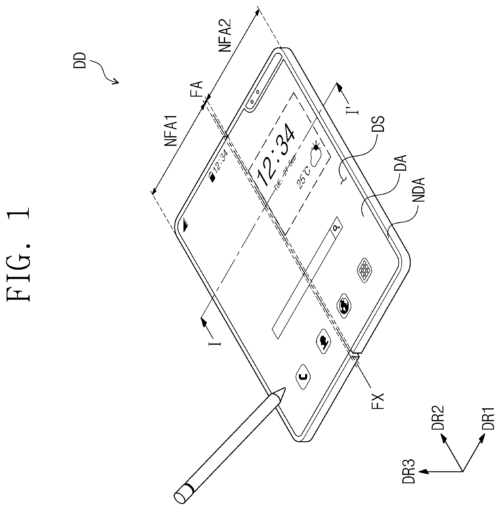
is a perspective view illustratively showing an embodiment of a display device DD. is a perspective view illustratively showing the display device DD illustrated in which is folded.
Referring to , a display device DD may be a device for generating and/or displaying an image. In an embodiment, for example, the display device DD may be a mobile phone. However, a type of the display device DD is not limited thereto. The display device DD may be another electronic apparatus for generating and/or displaying an image.
The display panel DD may have two short sides extending along a first direction DR 1 and long sides extending along a second direction DR 2 which crosses the first direction DR 1 . When viewed in a plan view, the display device DD may have a rectangular shape. However, the planar shape of the display device DD is not limited thereto. In an embodiment, for example, the display device DD may have a circular shape and a polygonal shape among planar shapes.
In this specification, the meaning of “when viewed in a plan view” or “in a plan view” may represent a view along a third direction DR 3 perpendicular or normal to a plane defined by the first direction DR 1 and the second direction DR 2 crossing each other.
The display device DD may include a display area DA and a non-display area NDA which is adjacent to the display area DA. In an embodiment, the non-display area NDA may surround the display area DA without being limited thereto. The display area DA may be a planar area at which an image is displayed. A display surface DS may define a top surface of the display device DD at the display area DA. The display device DD may provide an image to outside the display device DD, through the display surface DS. The non-display area NDA may be a planar area at which the image is not displayed. The non-display area NDA may be a bezel area of the display device DD.
According to an embodiment, the display device DD may be flexible, so as to be a flexible display device. In an embodiment, for example, the display device DD may be a foldable display device. The display device DD may be foldable and unfoldable about a folding axis FX.
In particular, the display device DD which is unfolded may include a first non-folding area NFA 1 , a folding area FA and a second non-folding area NFA 2 , which are arranged in order along the first direction DR 1 . The folding area FA may be disposed between the first non-folding area NFA 1 and the second non-folding area NFA 2 . The folding area FA may be a planar area at which the display device DD and various components thereof are foldable. A non-folding area may be a planar area at which the display device DD and various components thereof are unfoldable and/or which remain flat even when the display device DD is folded at the folding area FA.
In the embodiment, the display device DD is illustratively shown as having one of the folding area FA and two non-folding areas. However, the numbers of the folding area FA and the non-folding areas are not limited thereto. The display device DD may include more than two, for example, a plurality of non-folding areas and a plurality of folding areas respectively disposed between the non-folding areas.
Referring to , the display device DD may be folded about the folding axis FX. The folding axis FX may be a virtual line parallel to the second direction DR 2 . Here, in the display device DD which is folded, a top surface of the display device DD at the first non-folding area NFA 1 may face a top surface of the display device DD at the second non-folding area NFA 2 . Accordingly, the display surface DS of the display device DD may not be exposed to the outside. That is, the display device DD may be in-folded.
However, a folding operation of the display device DD is not limited thereto. In an embodiment, for example, the display device DD may be folded about a folding axis FX parallel to the first direction DR 1 . Also, the display device DD may be out-folded so that portions of the display surface DS face away from each other so as to be exposed to outside the display device DD.
is an exploded perspective view illustratively showing the display device DD illustrated in . is a cross-sectional view taken along line I-I′ of . is a cross-sectional view illustratively showing an embodiment of a display panel DP illustrated in . For convenience of description, adhesive layers disposed between layers of a display device DD are omitted in .
Referring to , the display device DD may include a display module DM, a digitizer module DTM, a first support layer SUP 1 , a reinforcing part RFP, a shielding sheet SSH, a second support layer SUP 2 and a compensation layer CPL.
The display module DM may be a flexible display module. In an embodiment, for example, the display module DM may be foldable or unfoldable about the folding axis FX (see ). The display module DM may include a first non-folding area NFA 1 , a folding area FA and a second non-folding area NFA 2 , which are arranged in order along a first direction DR 1 . Substantially, the first non-folding area NFA 1 , the folding area FA and the second non-folding area NFA 2 may be defined in each of the various components or layers of the display device DD (see ).
Referring to , the display module DM may include a display panel DP, an anti-reflection layer POL, a window WIN, a window protective layer WP and a cover layer CVL. Each of the layers of the display module DM may be a flexible layer.
The anti-reflection layer POL, the window WIN and the window protective layer WP may be disposed above the display panel DP in a third direction DR 3 .
The anti-reflection layer POL may be disposed on the display panel DP. The anti-reflection layer POL may be a film for reducing or effectively preventing external light from being reflected. The anti-reflection layer POL may reduce reflectivity of external light which is incident toward the display panel DP from above or outside the display device DD. In an embodiment, for example, the anti-reflection layer POL may include a phase retarder and/or a polarizer.
However, the anti-reflection layer POL is not limited thereto. The anti-reflection layer POL may be embodied with a color filter layer and a black matrix which are disposed on the display panel DP.
In particular, the external light may be filtered to have the same color as pixels within the display panel DP, by the color filter layer. In an embodiment, for example, the color filter layer may include red, green and blue color filters that correspond to pixels generating and/or emitting red, green and blue light, respectively. By the color filter layer, the external light may be filtered to have the red, green and blue light corresponding to the pixels. Consequently, the reflection of the external light is reduced or effectively prevented, and thus, the external light may not be viewed from outside the display device DD.
The window WIN may be disposed above the anti-reflection layer POL. The window WIN may protect the display panel DP and the anti-reflection layer POL from external scratches. An image generated in the display panel DP may pass through the window WIN and then be provided to outside of the display device DD. To this end, the window WIN may have optically transparent characteristics. In an embodiment, for example, the window WIN may include glass.
In the embodiment, the window WIN may be ultra-thin glass (“UTG”). However, the window WIN is not limited thereto. In an embodiment, for example, the window WIN may include transparent plastics.
The window WIN may have a multi-layer structure or a single-layer structure. In an embodiment, for example, the window WIN may include a plurality of synthetic resin films coupled by an adhesive, or a glass substrate and a synthetic resin film which are coupled to each other by an adhesive.
A first adhesive layer AU may be disposed between the window WIN and the anti-reflection layer POL. The window WIN may be attached to the anti-reflection layer POL by the first adhesive ALL In an embodiment, for example, the first adhesive layer AL 1 may be a pressure sensitive adhesive, but the type of the adhesive layer is not limited thereto. The first adhesive layer AL 1 may be another type of adhesive having optically transparent characteristics.
The window protective layer WP may be disposed on the window WIN. The window protective layer WP may include a flexible plastic material such as polyimide or polyethylene terephthalate. A second adhesive layer AL 2 may be disposed between the window protective layer WP and the window WIN. The second adhesive layer AL 2 may include the same material as the first adhesive layer AL 1 . The window protective layer WP may be attached to the window WIN by the second adhesive layer AL 2 .
The cover layer CVL may be disposed below the display panel DP. The cover layer CVL may define a lower portion or lower surface of the display module DM. The cover layer CVL may absorb external shocks applied from below the display module DM. In an embodiment, for example, the cover layer CVL may include a barrier layer and a cushion layer.
The barrier layer may increase resistance to compression due to external pressing. In an embodiment, for example, the barrier layer may have a role in reducing or effectively preventing deformation of the display panel DP. The barrier layer may include a flexible plastic material such as polyimide or polyethylene terephthalate.
The cushion layer may absorb the external shocks applied from below the display module DM to protect the display module DM. To this end, the cushion layer may include a foam sheet having a predetermined elastic force. The cushion layer may include foam, sponge, polyurethane or thermoplastic polyurethane.
Referring to , the display panel DP may include a substrate SUB, a circuit element layer CL disposed on the substrate SUB, a display element layer OL disposed on the circuit element layer CL, a thin film encapsulation layer TFE (e.g., encapsulation layer) disposed on the display element layer OL, and an input sensing layer ISP disposed on the thin film encapsulation layer TFE.
The substrate SUB may include a flexible plastic material. In an embodiment, for example, the substrate SUB may include polyimide (“PI”). However, the material of the substrate SUB is not limited thereto.
The circuit element layer CL may include an insulating layer, a semiconductor pattern and a conductive pattern, a signal line and the like. The insulating layer, the semiconductor layer and the conductive layer are provided or formed on the substrate SUB through coating and deposition methods, and subsequently, the insulating layer, the semiconductor layer and the conductive layer may be selectively patterned through photolithography processes performed multiple times. Subsequently, the semiconductor pattern, the conductive pattern, and the signal line of the circuit element layer CL may be provided or formed.
The display element layer OL may be disposed corresponding to the display area DA. The display element layer OL may include a light emitting element as a display element. In an embodiment, for example, the display element layer OL may include an organic light emitting material, a quantum dot, a quantum rod or micro light emitting diode (“LED”) as a display element.
The thin film encapsulation layer TFE may be disposed on the circuit element layer CL to cover the display element layer OL. The thin film encapsulation layer TFE may include an inorganic layer, an organic layer and an inorganic layer which are sequentially stacked along the third direction DR 3 . The inorganic layer may include an inorganic material and protect pixels from moisture/oxygen. The organic layer may include an organic material and protect pixels from impurities such as dust particles.
The input sensing layer ISP may include a plurality of sensors (not shown) for sensing an external input. The sensors may sense the external input in a capacitive method. The external input may include various types of inputs or input tools such as a portion of a body, light, heat, a pen or pressure.
The input sensing layer ISP may be disposed directly on the thin film encapsulation layer TFE when the display panel DP is manufactured. However, the invention is not limited thereto. The input sensing layer ISP may include or be made of a panel independent of the display panel DP and attached to the display panel DP by a separate member such as an adhesive layer.
In the preceding description, the display panel DP is assumed to be an organic light emitting display panel, but the invention is not limited thereto. In an embodiment, for example, the display device DD may be a liquid crystal display device.
Referring to again, the digitizer module DTM may be disposed below the display module DM. Particularly, the digitizer module DTM may be disposed below the cover layer CVL. The digitizer module DTM may be bonded to the cover layer CVL by a third adhesive layer AL 3 having an adhesive component.
The digitizer module DTM may be a flexible layer. The digitizer module DTM may be foldable together with the display module DM.
The digitizer module DTM is a device through which position information from the display surface DS is input. The digitizer module DTM may be embodied in an electromagnetic method (or an electromagnetic resonance method). In an embodiment, for example, the digitizer module DTM may include a digitizer sensor substrate (not shown) including a plurality of coils.
When an input tool such as a pen is proximate to and moved along the display device DD (see ), the pen is driven by an alternating electrical current signal to generate an oscillating magnetic field, and an electrical signal may be induced in a coil by the oscillating magnetic field. A position of the pen along the display panel DP may be detected through the electrical signal induced in the coil. The digitizer module DTM may detect an electromagnetic change caused by the approach of the pen to identify the position of the pen with respect to the display device DD, such as a position along the display panel DP. The digitizer module DTM may otherwise be a position detector layer.
According to an embodiment, the first support layer SUP 1 may be disposed below the digitizer module DTM. The first support layer SUP 1 may support the display module DM and the digitizer module DTM. The first support layer SUP 1 may face the display module DM with the digitizer module DTM therebetween. The first support layer SUP 1 may be exposed outside of the display device DD, at the folding area FA, without being limited thereto.
The first support layer SUP 1 may be bonded to the digitizer module DTM by a fourth adhesive layer AL 4 having an adhesive component. Although illustrates that the fourth adhesive layer AL 4 is disposed even in a region overlapping or corresponding to the folding area FA, the fourth adhesive layer AL 4 may be disposed only in regions overlapping or corresponding to the first non-folding area NFA 1 and the second non-folding area NFA 2 .
The first support layer SUP 1 may be a flexible layer. In an embodiment, for example, the first support layer SUP 1 may include a metal material such as stainless steel. The first support layer SUP 1 may be foldable together with the display module DM and the digitizer module DTM.
When viewed in a plan view, a surface area of the first support layer SUP 1 may be greater than each of a surface area of the display module DM and a surface area of the digitizer module DTM. Particularly, one or both of opposing ends of the first support layer SUP 1 may protrude further outward along the first direction DR 1 than corresponding ends of the display module DM and corresponding ends of the digitizer module DTM. Ends of the aforementioned components may define an edge of respective components, such as an outer edge thereof.
According to an embodiment, since an edge of the first support layer SUP 1 protrudes further outward than corresponding edges of the display module DM and the digitizer module DTM, the first support layer SUP 1 may effectively protect the display module DM and the digitizer module DTM against shocks applied from outside of the display device DD.
According to an embodiment, the first support layer SUP 1 may include a first section PP 1 (e.g., first portion or first planar area), a second section PP 2 (e.g., second portion or second planar area), and a third section PP 3 (e.g., third portion or third planar area), which are arranged along the first direction DR 1 . The third section PP 3 may be disposed between the first section PP 1 and the second section PP 2 . The first to third sections PP 1 to PP 3 may be integrated with each other in to a single one of the first support layer SUP 1 . Each of the aforementioned planar areas may have dimensions along the first direction DR 1 and the second direction DR 2 . In an embodiment, a width may be defined along the first direction DR 2 , without being limited thereto.
The first section PP 1 may overlap or correspond to the first non-folding area NFA 1 . The second section PP 2 may overlap or correspond to the second non-folding area NFA 2 . A first hole H 1 may be defined in each of the first section PP 1 and the second section PP 2 . The first hole H 1 may be provided in plurality including a plurality of first holes H 1 . Portions of the first support layer SUP 1 at the first section PP 1 and the second section PP 2 may define the first hole H 1 . The first hole H 1 may extend through a thickness of the first support layer SUP 1 . The first hole H 1 of the first support layer SUP 1 may be open at one or both surfaces thereof among an upper surface closest to the display module DM and a lower surface furthest from the display module DM.
The third section PP 3 may overlap or correspond to the folding area FA. A second hole H 2 may be defined in the third section PP 3 . The second hole H 2 may be provided in plurality including a plurality of second holes H 2 . Portions of the first support layer SUP 1 at the third section PP 3 may define the second hole H 2 . The second hole H 2 may extend through a thickness of the first support layer SUP 1 . The first hole H 1 of the first support layer SUP 1 may be open at one or both surfaces thereof among the upper surface and the lower surface thereof.
According to an embodiment, a reinforcing part RFP may be disposed below the first support layer SUP 1 . The reinforcing part RFP may include a nonmetallic lightweight material. In an embodiment, for example, the reinforcing part RFP may include a plastic material.
The reinforcing part RFP may include a reinforcing layer RFL and a plurality of dummies DU (e.g., reinforcing protrusions). The reinforcing layer RFL (e.g., reinforcing body) may include a first reinforcing layer RFL 1 (e.g., first reinforcing body) and a second reinforcing layer RFL 2 (e.g., second reinforcing body). The first reinforcing layer RFL 1 may be disposed below the first section PP 1 and overlap the first non-folding area NFA 1 . The second reinforcing layer RFL 2 may be disposed below the second section PP 2 and overlap the second non-folding area NFA 2 . The reinforcing layer RFL may be disconnected at the folding area FA. That is, within the reinforcing layer RFL, the first reinforcing body may be disconnected from the second reinforcing body, at the folding area FA.
The plurality of dummies DU may be respectively disposed in the first holes H 1 which are defined in the first section PP 1 and the second section PP 2 of the first supporting layer SUP 1 . The first support layer SUP 1 and the reinforcing part RFP will be described later in detail.
According to an embodiment, the shielding sheet SSH (e.g., shielding layer) may be disposed below the reinforcing part RFP. The shielding sheet SSH may absorb electromagnetic waves to improve operation reliability of the digitizer module DTM. The shielding sheet SSH may define an electromagnetic wave absorbing layer. In an embodiment, for example, the shielding sheet SSH may include magnetic metal powder (“MMP”). However, the material of the shielding sheet SSH is not limited thereto. In an embodiment, for example, the shielding sheet SSH may include a metal material having high permeability. The shielding sheet SSH may be disconnected at the folding area FA.
The shielding sheet SSH may include a first shielding sheet SSH 1 (e.g., first electromagnetic wave absorbing sheet) and a second shielding sheet SSH 2 (e.g., second electromagnetic wave absorbing sheet). The first shielding sheet SSH 1 may be disposed below the first reinforcing layer RFL 1 . The first shielding sheet SSH 1 may be bonded to the first reinforcing layer RFL 1 by a fifth adhesive layer AL 5 (e.g., adhesive pattern).
The first shielding sheet SSH 1 may overlap the first non-folding area NFA 1 and a first portion of the folding area FA. More particularly, a first end SSH 1 -E of the first shielding sheet SSH 1 may protrude further along the first direction DR 1 than does the second end RFL 1 -E of the first reinforcing layer RFL 1 . Accordingly, a stepped structure may be provided between the first reinforcing layer RFL 1 and the first shielding sheet SSH 1 .
The second shielding sheet SSH 2 may be disposed below the second reinforcing layer RFL 2 . The second shielding sheet SSH 2 may be spaced apart from the first shielding sheet SSH 1 along the first direction DR 1 . That is, the first shielding sheet SSH 1 and the second shielding sheet SSH 2 may be disconnected from the second reinforcing body, at the folding area FA. The second shielding sheet SSH 2 may be bonded to the second reinforcing layer RFL 2 by the fifth adhesive layer AL 5 . The adhesive patterns defined by the fifth adhesive layer may also be disconnected from each other at the folding area FA.
The second shielding sheet SSH 2 may overlap the second non-folding area NFA 2 and a second portion of the folding area FA. More particularly, a third end SSH 2 -E of the second shielding sheet SSH 2 may protrude further along the first direction DR 1 than does a fourth end RFL 2 -E of the second reinforcing layer RFL 2 . Accordingly, a stepped structure may be provided between the second reinforcing layer RFL 2 and the second shielding sheet SSH 2 .
The second support layer SUP 2 may be disposed below the shielding sheet SSH. The second support layer SUP 2 may support the first non-folding area NFA 1 and the second non-folding area NFA 2 of the display module DM. The second support layer SUP 2 may include a rigid material. In an embodiment, for example, the second support layer SUP 2 may include a metal material such as stainless steel. However, this is described as an example, and the second support layer SUP 2 may include various metals (for example, an Invar alloy).
The second support layer SUP 2 may include a first plate PL 1 and a second plate PL 2 arranged along the first direction DR 1 , and the second plate PL 2 is spaced apart from the first plate PL 1 along the first direction DR 1 . That is, the second support layer SUP 2 is disconnected at the folding area FA. The first plate PL 1 may be disposed below the first shielding sheet SSH 1 and overlap the first non-folding area NFA 1 and a portion of the folding area FA. The second plate PL 2 may be disposed below the second shielding sheet SSH 2 and overlap the second non-folding area NFA 2 and a portion of the folding area FA. That is the first plate PL 1 and the second plate PL 2 may be disconnected from each other at the folding area FA.
According to an embodiment, the compensation layer CPL may be disposed between the shielding sheet SSH and the first support layer SUP 1 . The compensation layer CPL may be disconnected at the folding area FA. The compensation layer CPL may overlap or correspond to the folding area FA. Particularly, the compensation layer CPL may include a first compensation layer CPL 1 and a second compensation layer CPL 2 . The first compensation layer CPL 1 and the second compensation layer CPL 2 may be disconnected from each other at the folding area FA. The first compensation layer CPL 1 and the second compensation layer CPL 2 may be respectively spaced apart from the second end RFL 1 -E and the fourth end RFL 2 -E.
The first compensation layer CPL 1 may be disposed between the first shielding sheet SSH 1 and the third section PP 3 of the first support layer SUP 1 . The second compensation layer CPL 2 may be disposed between the second shielding sheet SSH 2 and the third section PP 3 of the first support layer SUP 1 . The first compensation layer CPL 1 and the second compensation layer CPL 2 may be fixed to the first shielding sheet SSH 1 and the second shielding sheet SSH 2 , respectively. A distal end of the compensation layer CPL is furthest from the shielding sheet SSH and closest to the first support layer SUP 1 . The distal end of the compensation layer CPL is non-fixed or detachable from the shielding sheet SSH to be separable therefrom.
According to an embodiment, the compensation layer CPL (e.g., support member or support pattern) may support the third section PP 3 of the first support layer SUP 1 . Thus, when an external force is applied to the folding area FA from above the display device DD, the compensation layer CPL may reduce or effectively prevent deformation of layers at the folding area FA.
is an enlarged plan view illustrating region A 1 of the first support layer SUP 1 shown in . is an enlarged plan view illustrating region A 2 of the reinforcing layer RFL shown in . When viewed in a plan view, the region A 1 and the region A 2 may overlap each other or be aligned with each other along the third direction DR 3 .
Referring to , the plurality of first holes H 1 may be defined in each of the first section PP 1 and the second section PP 2 of the first support layer SUP 1 . The first holes H 1 may overlap the first and second non-folding areas NFA 1 and NFA 2 . The first holes H 1 may not overlap the folding area FA.
When viewed in a plan view, each of the first holes H 1 may have a planar shape such as a rectangular shape extending elongated along the first direction DR 1 . The first holes H 1 may be defined as passing through the first section PP 1 and the second section PP 2 of the first support layer SUP 1 along a third direction DR 3 . As passing through, the first holes H 1 may be extended completely through a thickness of a body of the support layer SUP 1 along the third direction DR 3 , without being limited thereto.
The first holes H 1 may be arranged along the first direction DR 1 and along the second direction DR 2 . The first holes H 1 which neighbor each other may be spaced apart from each other along the first direction DR 1 and along the second direction DR 2 . However, the planar shape and arrangement of the first holes H 1 along the first support layer SUP 1 are not limited to those described above.
A lattice pattern may be defined within the third section PP 3 . Particularly, the third section PP 3 may include a first branch BR 1 provided in plurality including a plurality of the first branches BR 1 and a second branch BR 2 provided in plurality including a plurality of second branches BR 2 . Each of the first branches BR 1 may lengthwise extend along the second direction DR 2 . The first branches BR 1 may be parallel to the folding axis FX illustrated in . Although only five of the first branches BR 1 are illustrated in for convenience of description, the invention is not limited thereto. In an embodiment, the number of the first branches BR 1 may be higher than five.
The second branches BR 2 may be disposed between the first branches BR 1 . Particularly, each of the second branches BR 2 may extend lengthwise along the first direction DR 1 . The second branch BR 2 may extend from portions of the first branches BR 1 which are adjacent to each other along the first direction DR 1 . The first branches BR 1 may be connected to each other by the second branches BR 2 .
The second branches BR 2 may be disposed between the first section PP 1 and the first branch BR 1 which is closest to the first section PP 1 among the first branches BR 1 . The second branches BR 2 may be disposed between the second section PP 2 and the first branch BR 1 which is closest to the second section PP 2 among the first branches BR 1 . Consequently, the third section PP 3 may be connected to each of the first section PP 1 and the second section PP 2 at the second branches BR 2 .
Second holes H 2 may be defined in the first branches BR 1 . In an embodiment, for example, the plurality of second holes H 2 (see ) may be defined by solid portions of the first support layer SUP 1 at each of the first branches BR 1 . Each of the second holes H 2 may extend elongated along the second direction DR 2 . However, the planar shape of the second holes H 2 is not limited thereto. The second holes H 2 may pass through the solid portions of the first support layer SUP 1 at the first branches BR 1 , along the third direction DR 3 .
According to the embodiment, since the lattice pattern is defined in the third section PP 3 of the first support layer SUP 1 which overlaps the folding area FA, the folding operation of the display device DD may be easily performed.
Referring to , the first reinforcing layer RFL 1 may be disposed below the first section PP 1 of the first support layer SUP 1 . The first reinforcing layer RFL 1 may overlap the first non-folding area NFA 1 . The first reinforcing layer RFL 1 may not overlap the folding area FA.
The second reinforcing layer RFL 2 may be disposed below the second section PP 2 of the first support layer SUP 1 . The second reinforcing layer RFL 2 may overlap the second non-folding area NFA 2 . The second reinforcing layer RFL 2 may not overlap the folding area FA.
The second reinforcing layer RFL 2 may be spaced apart from the first reinforcing layer RFL 1 along the first direction DR 1 . In an embodiment, for example, the second reinforcing layer RFL 2 may be spaced a distance D from the first reinforcing layer RFL 1 along the first direction DR 1 . The distance D may be the same as a width of the third section PP 3 along the first direction DR 1 illustrated in . That is, an inner edge of each of the first reinforcing layer RFL 1 and the second reinforcing layer RFL 2 may be aligned with respective boundaries of the third section PP 3 with the first section PP 1 and the second section PP 2 .
The first reinforcing layer RFL 1 and the second reinforcing layer RFL 2 may include a nonmetallic material. In an embodiment, for example, the first reinforcing layer RFL 1 and the second reinforcing layer RFL 2 may include a plastic material.
According to an embodiment, the dummies DU may extend from a top surface of the reinforcing layer RFL. A top surface of the reinforcing layer may face the display module DM and be common to each of the dummies DU. The dummies DU may be extended into the first holes H 1 of the first support layer SUP 1 . The dummies DU may include a nonmetallic material. In an embodiment, for example, the dummies DU may include a plastic material.
More particularly, the dummies DU may include first dummies DU 1 (e.g., first reinforcing protrusions) and second dummies DU 2 (e.g., second reinforcing protrusions). The first dummies DU 1 may extend from the top surface of the first reinforcing layer RFL 1 . The first dummies DU 1 may be extended into the first holes H 1 defined in the first section PP 1 of the first support layer SUP 1 .
Each of the first dummies DU 1 may have a shape corresponding to a shape of the first holes H 1 . In an embodiment, for example, when viewed in a plan view, each of the first dummies DU 1 may have a rectangular shape. That is, the first dummies DU 1 of the reinforcing part RFP engage with respective holes of the first support layer SUP 1 . Taking , 6 and 7 together, the first dummies DU 1 may fill the respective holes of the first support layer SUP 1 . A distal end of the first dummies DU 1 which is furthest from a respective reinforcing layer may be coplanar with the upper surface of the first support layer SUP 1 , without being limited thereto.
The second dummies DU 2 may extend from the top surface of the second reinforcing layer RFL 2 . The second dummies DU 2 may be extended into the first holes H 1 defined in the second section PP 2 of the first support layer SUP 1 .
Each of the second dummies DU 2 may have a shape corresponding to a shape of the first holes H 1 . In an embodiment, for example, when viewed in a plan view, each of the second dummies DU 2 may have a rectangular shape. That is, the second dummies DU 2 of the reinforcing part RFP engage with respective holes of the first support layer SUP 1 . Taking , 6 and 7 together, the second dummies DU 2 may fill the respective holes of the first support layer SUP 1 . A distal end of the second dummies DU 2 which is furthest from a respective reinforcing layer may be coplanar with the upper surface of the first support layer SUP 1 , without being limited thereto.
According to an embodiment, the plurality of first holes H 1 which are defined in the first support layer SUP 1 including a metal material, may reduce or effectively prevent generation of an electrical eddy current between the digitizer module DTM and the shielding sheet SSH including an electromagnetic wave absorbing material such as a metal material. Accordingly, the sensitivity of the digitizer module DTM may be improved.
According to an embodiment, since the dummies DU are respectively disposed in the first holes H 1 of the first support layer SUP 1 , the first holes H 1 may not be viewable from outside the first support layer SUP 1 or outside of the display device DD.
According to an embodiment, the plurality of first holes H 1 are defined in the first support layer SUP 1 including the metal material, and the dummies DU having a relatively lighter weight than the metal material as including a nonmetallic material are respectively disposed in the first holes H 1 . Thus, a total weight of the display device DD may be reduced.
is a cross-sectional view taken along line II-II′ of . For convenience of description, the display module DM is schematically illustrated in . Hereinafter, a structure of each of the layers of the display device DD in the display device DD which is folded will be described with reference to .
Referring to , the display module DM may be foldable at the folding area FA about the folding axis FX. Accordingly, in the display device DD which is folded, the first non-folding area NFA 1 may be disposed above the second non-folding area NFA 2 to be furthest along the third direction DR 3 . The display device DD which is folded may dispose the first non-folding area NFA 1 and the second non-folding area NFA 2 parallel to each other.
The digitizer module DTM and the first support layer SUP 1 may be foldable together with the display module DM. Particularly, the third section PP 3 of the first support layer SUP 1 may be foldable together with display module DM and the digitizer module DTM at the folding area FA. The first section PP 1 may be movable together with the first non-folding area NFA 1 . Accordingly, the first section PP 1 may be disposed above the second section PP 2 along the thickness direction of the display device DD which is folded. The display device DD which is folded may dispose the first section PP 1 and the second section PP 2 parallel to each other. In the display device DD which is folded, the third section PP 3 may define an end portion of the display device DD, without being limited thereto.
According to an embodiment, the first reinforcing layer RFL 1 may be movable together with the first section PP 1 of the first support layer SUP 1 . The display device DD which is folded may dispose the first reinforcing layer RFL 1 parallel to the first section PP 1 . The second reinforcing layer RFL 2 may be movable together with the second section PP 2 of the first support layer SUP 1 . The display device DD which is folded may dispose the second reinforcing layer RFL 2 parallel to the second section PP 2 .
According to an embodiment of the display device DD which is folded, the first shielding sheet SSH 1 may be movable together with the first reinforcing layer RFL 1 and be disposed parallel to the first reinforcing layer RFL 1 . The second shielding sheet SSH 2 may be movable together with the second reinforcing layer RFL 2 and be disposed parallel to the second reinforcing layer RFL 2 within the display device DD which is folded.
According to an embodiment of the display device DD which is folded, the first plate PL 1 of the second support layer SUP 2 may be movable together with the first shielding sheet SSH 1 and be disposed parallel to the first shielding sheet SSH 1 . Also, the second plate PL 2 may be movable together with the second shielding sheet SSH 2 and be disposed parallel to the second shielding sheet SSH 2 within the display device DD which is folded.
According to an embodiment, the first compensation layer CPL 1 and the second compensation layer CPL 2 may be movable together with the first shielding sheet SSH 1 and the second shielding sheet SSH 2 , respectively. In an embodiment, the display panel DP which is folded disposes the compensation layer CPL attached to the electromagnetic wave absorbing layer and detached from the first support layer SUP 1 .
In the display device DD which is unfolded ( ), layers or patterns which are disconnected from each other may be coplanar with each other, without being limited thereto. According to an embodiment, the first shielding sheet SSH 1 movable together with the first non-folding area NFA 1 is provided separated from the second shielding sheet SSH 2 movable together with the second non-folding area NFA 2 , and thus, damage to the shielding sheet SSH by folding and unfolding of the display device DD may be reduced or effectively prevented.
to 11 are top plan views illustratively showing embodiment of a first support layer SUP 1 of a display device DD. In display devices according to the following embodiments, components except for the first support layer SUP 1 and the reinforcing layer RFL are the same as the components of the embodiments described above.
Hereinafter, descriptions of the same components will be omitted, and differences will be mainly described.
Referring to , a first hole H 1 - 1 may be defined in each of a first section PP 1 and a second section PP 2 of a first support layer SUP 1 - 1 . The first holes H 1 - 1 may be provided in plurality. When viewed in a plan view, each of the first holes H 1 - 1 may have a circular shape as a planar shape. The first holes H 1 - 1 arranged along a first direction DR 1 may be disposed alternately with each other along a second direction DR 2 . Consequently, the first holes H 1 - 1 may be arranged in a zigzag pattern.
Dummies DU of the reinforcing part RFP may be respectively disposed in the first holes H 1 - 1 . The dummies DU may have a shape corresponding to a shape the first holes H 1 - 1 . When viewed in a plan view, each of dummies DU of the reinforcing part RFP may have a circular shape.
Referring to , a first hole H 1 - 2 may be provided in plurality including first holes H 1 - 2 defined in each of a first section PP 1 and a second section PP 2 of a first support layer SUP 1 - 2 . The first holes H 1 - 2 may be arranged along a first direction DR 1 and along a second direction DR 2 . The first holes H 1 - 2 which are adjacent to each other may be spaced apart from each other along the first direction DR 1 and/or the second direction DR 2 . When viewed in a plan view, each of the first holes H 1 - 2 may have a square shape.
Dummies DU of the reinforcing part RFP may be disposed in the first holes H 1 - 2 . The dummies DU may have a shape corresponding to a shape the first holes H 1 - 2 . When viewed in a plan view, each of the dummies DU of the reinforcing part RFP may have a square shape.
Referring to , a first hole H 1 - 3 may be provided in plurality including first holes H 1 - 3 defined in each of a first section PP 1 and a second section PP 2 of a first support layer SUP 1 - 3 . The first holes H 1 - 3 may be arranged in a first direction DR 1 and a second direction DR 2 . Each of the first holes H 1 - 3 may extend elongated along a second direction DR 2 . When viewed in a plan view, each of the first holes H 1 - 3 may have a rectangular shape.
Dummies DU of the reinforcing part RFP may be disposed in the first holes H 1 - 3 . The dummies DU may have a shape corresponding to a shape the first holes H 1 - 3 . When viewed in a plan view, each of the dummies DU of the reinforcing part RFP may have a rectangular shape.
According to one or more embodiment, generation of an electrical eddy current between the digitizer module DTM and the shielding sheet SSH is suppressed by the plurality of first holes H 1 defined in the first support layer SUP 1 , and thus, the sensitivity of the digitizer module DTM may be improved.
Also, according to one or more embodiment, the plurality of first holes H 1 are defined in the first support layer SUP 1 including the metal material and the dummies DU having a relatively lighter weight than the metal material are disposed in the first holes H 1 . Thus, a total weight of the display device DD may be reduced.
Although the embodiments have been described, it is understood that various changes and modifications can be made by one ordinary skilled in the art within the spirit and scope of the disclosure as hereinafter claimed. Also, the embodiments are not intended to limit the technical ideas of the disclosure, and all technical ideas within the following claims and their equivalents should be interpreted to be included in the scope of right in the disclosure.
Figures (11)
Citations
This patent cites (28)
- US10164208
- US10541373
- US10686246
- US11513415
- US11610520
- US12014018
- US2016/0084994
- US2018/0341290
- US2019/0131553
- US2019/0267430
- US2019/0334114
- US2019/0355927
- US2020/0166970
- US2020/0209998
- US2020/0389986
- US2021/0118337
- US2021/0168929
- US2021/0174711
- US2021/0311525
- US2021/0365132
- US2021/0385959
- US2021/0407344
- US1020150051054
- US1020180079091
- US1020190101584
- US1020190124844
- US1020190131154
- US1020200084495