Pressure Sensor Including a Pressure Sensor Chip to Detect a Differential Pressure with High Accuracy
Abstract
A pressure sensor chip includes a third conductive layer, a second insulating layer, a first conductive layer, a first insulating layer, and a second conductive layer stacked in order. The first insulating layer includes first and second cavities communicating externally. The second insulating layer includes third and fourth cavities respectively communicating with the second and first cavities. The first conductive layer includes first and second diaphragms, the second conductive layer includes first and second electrodes, and the third conductive layer includes third and fourth electrodes. The first diaphragm and the first electrode face each other with the cavity interposed therebetween, the second diaphragm and the electrode face each other with the first cavity interposed therebetween, the first diaphragm and the third electrode face each other with the fourth cavity interposed therebetween, and the second diaphragm and the fourth electrode face each other with the fourth cavity interposed therebetween.
Claims (20)
1. A pressure sensor chip, comprising: a first insulating layer including a first cavity and a second cavity, and being electrically insulated; a second insulating layer including a third cavity and a fourth cavity, and being electrically insulated; a first conductive layer between the first insulating layer and the second insulating layer; a second conductive layer joined to the first insulating layer on an opposite side from the first conductive layer; a third conductive layer joined to the second insulating layer on an opposite side from the first conductive layer; a first flow path through which the first cavity and the fourth cavity communicate with each other; a second flow path through which the second cavity and the third cavity communicate with each other; a first communication portion through which at least one of the first cavity and the fourth cavity communicates externally; and a second communication portion through which at least one of the second cavity and the third cavity communicates externally; wherein the first conductive layer includes: a first diaphragm between the first cavity and the third cavity; and a second diaphragm between the second cavity and the fourth cavity; the second conductive layer includes: a first electrode facing the first diaphragm with the first cavity interposed therebetween; and a second electrode facing the second diaphragm with the second cavity interposed therebetween; and the third conductive layer includes: a third electrode facing the first diaphragm with the third cavity interposed therebetween; and a fourth electrode facing the second diaphragm with the fourth cavity interposed therebetween.
Show 19 dependent claims
2. The pressure sensor chip according to claim 1 , wherein in plan view of the first conductive layer, the first diaphragm and the second diaphragm have a same or substantially a same area.
3. The pressure sensor chip according to claim 1 , wherein the first insulating layer and the second insulating layer have a same or substantially a same thickness.
4. The pressure sensor chip according to claim 1 , further comprising: a first pad electrically connected to the first electrode; a second pad electrically connected to the second electrode; a third pad electrically connected to the third electrode; a fourth pad electrically connected to the fourth electrode; and a fifth pad electrically connected to the first diaphragm and the second diaphragm.
5. The pressure sensor chip according to claim 1 , further comprising: a first pad electrically connected to the first electrode and the fourth electrode; a second pad electrically connected to the second electrode and the third electrode; a third pad electrically connected to the first diaphragm, and a fourth pad electrically connected to the second diaphragm.
6. The pressure sensor chip according to claim 1 , wherein the first flow path includes: a first through-hole in the first conductive layer; a first space in the first insulating layer and communicating with the first through-hole and the first cavity; and a second space in the second insulating layer and communicating with the first through-hole and the fourth cavity.
7. The pressure sensor chip according to claim 1 , wherein the second flow path includes: a second through-hole in the first conductive layer; a third space in the first insulating layer and communicating with the second through-hole and the second cavity; and a fourth space in the second insulating layer, and communicating with the second through-hole and the third cavity.
8. The pressure sensor chip according to claim 1 , wherein the second conductive layer is exposed externally, and includes the first communication portion and the second communication portion.
9. The pressure sensor chip according to claim 1 , further comprising: a first base portion including at least one layer, and joined to the second conductive layer on an opposite side from the first insulating layer; and a second base portion including at least one layer, and joined to the third conductive layer on an opposite side from the second insulating layer; wherein the first base portion and the second base portion are symmetrical or substantially symmetrical to each other with respect to the first conductive layer.
10. The pressure sensor chip according to claim 9 , wherein at least one of the first base portion and the second base portion includes a conductive layer.
11. A pressure sensor, comprising: the pressure sensor chip according to claim 1 ; and a control chip electrically connected to the first electrode, the second electrode, the third electrode, the fourth electrode, the first diaphragm, and the second diaphragm; wherein the control chip is configured or programmed to calculate a differential pressure between pressure applied to the first diaphragm and pressure applied to the second diaphragm, based on signals from the first electrode, the second electrode, the third electrode, the fourth electrode, the first diaphragm, and the second diaphragm.
12. The pressure sensor according to claim 11 , wherein in plan view of the first conductive layer, the first diaphragm and the second diaphragm have a same or substantially a same area.
13. The pressure sensor according to claim 11 , wherein the first insulating layer and the second insulating layer have a same or substantially a same thickness.
14. The pressure sensor according to claim 11 , further comprising: a first pad electrically connected to the first electrode; a second pad electrically connected to the second electrode; a third pad electrically connected to the third electrode; a fourth pad electrically connected to the fourth electrode; and a fifth pad electrically connected to the first diaphragm and the second diaphragm.
15. The pressure sensor according to claim 11 , further comprising: a first pad electrically connected to the first electrode and the fourth electrode; a second pad electrically connected to the second electrode and the third electrode; a third pad electrically connected to the first diaphragm, and a fourth pad electrically connected to the second diaphragm.
16. The pressure sensor according to claim 11 , wherein the first flow path includes: a first through-hole in the first conductive layer; a first space in the first insulating layer and communicating with the first through-hole and the first cavity; and a second space in the second insulating layer and communicating with the first through-hole and the fourth cavity.
17. The pressure sensor according to claim 11 , wherein the second flow path includes: a second through-hole in the first conductive layer; a third space in the first insulating layer and communicating with the second through-hole and the second cavity; and a fourth space in the second insulating layer, and communicating with the second through-hole and the third cavity.
18. The pressure sensor according to claim 11 , wherein the second conductive layer is exposed externally, and includes the first communication portion and the second communication portion.
19. The pressure sensor according to claim 11 , further comprising: a first base portion including at least one layer, and joined to the second conductive layer on an opposite side from the first insulating layer; and a second base portion including at least one layer, and joined to the third conductive layer on an opposite side from the second insulating layer; wherein the first base portion and the second base portion are symmetrical or symmetrical to each other with respect to the first conductive layer.
20. The pressure sensor according to claim 19 , wherein at least one of the first base portion and the second base portion includes a conductive layer.
Full Description
Show full text →
CROSS REFERENCE TO RELATED APPLICATIONS
This application claims the benefit of priority to Japanese Patent Application No. 2020-171848 filed on Oct. 12, 2020 and is a Continuation Application of PCT Application No. PCT/JP2021/032694 filed on Sep. 6, 2021. The entire contents of each application are hereby incorporated herein by reference.
BACKGROUND OF THE INVENTION
1. Field of the Invention
The present invention relates to a pressure sensor chip for measuring an external pressure, and a pressure sensor including the pressure sensor chip.
2. Description of the Related Art
A known pressure sensor detects an external pressure. Various types of influence exerted on the pressure sensor may cause an error in a detected pressure. Examples of such influence include impact applied to the pressure sensor from outside, a change in elasticity due to deterioration caused by aging of a material forming the pressure sensor, and the like.
In order to solve the above-described problem, in a pressure sensor disclosed in Japanese Unexamined Patent Application Publication No. 6-201419, a space on a front surface side of one film of two films that are deformed in accordance with an applied pressure and a space on a rear surface side of another film of the two films are made to communicate with each other. In addition, in the pressure sensor, a space on a rear surface side of the one film and a space on a front surface side of the other film are made to communicate with each other. Thus, when pressure is applied to the two films, the two films are deformed in directions opposite to each other, and accordingly an error in a detected pressure caused by the above-described various types of influence is canceled out and reduced.
As one type of pressure sensor, a capacitive differential pressure sensor capable of measuring a differential pressure between two pressures has been known. Such a differential pressure sensor includes a first conductive layer in which two diaphragms (a first diaphragm and a second diaphragm) are formed, and a second conductive layer facing the first conductive layer. A differential pressure between two pressures is detected by subtracting a capacitance value between the second diaphragm and the second conductive layer from a capacitance value between the first diaphragm and the second conductive layer.
When a configuration of the pressure sensor disclosed in Japanese Unexamined Patent Application Publication No. 6-201419 is applied to such a differential pressure sensor, a first pressure is applied to the first diaphragm from a side of the second conductive layer, and a second pressure is applied to the first diaphragm from an opposite side from the second conductive layer. In addition, the second pressure is applied to the second diaphragm from the side of the second conductive layer, and the first pressure is applied to the second diaphragm from the opposite side from the second conductive layer. Accordingly, since the first diaphragm and the second diaphragm are bent in directions opposite to each other, similar effects as those of the pressure sensor disclosed in Japanese Unexamined Patent Application Publication No. 6-201419 can be obtained. However, problems described below may occur.
A material forming the differential pressure sensor may be warped or solidified due to a change in temperature. The change in temperature occurs when a process of rapidly increasing or decreasing temperature is performed when manufacturing the differential pressure sensor, when a reflow process is performed when mounting the manufactured differential pressure sensor on a substrate, or the like. In addition, an elastic modulus of the material forming the differential pressure sensor may change due to moisture absorption or the like.
When the first conductive layer (the first diaphragm and the second diaphragm) of the differential pressure sensor is warped, solidified, or changed in elastic modulus as described above, stress is applied to the first conductive layer. When the stress affects the bending of the first diaphragm and the second diaphragm, an error may occur in each capacitance value. This may result in an error becoming greater in a detected differential pressure.
SUMMARY OF THE INVENTION
Preferred embodiments of the present invention provide pressure sensor chips each able to detect a differential pressure with high accuracy.
A pressure sensor chip according to a preferred embodiment of the present invention includes a first insulating layer including a first cavity and a second cavity, and being electrically insulated, a second insulating layer including a third cavity and a fourth cavity, and being electrically insulated, a first conductive layer between the first insulating layer and the second insulating layer, a second conductive layer joined to the first insulating layer on an opposite side from the first conductive layer, a third conductive layer joined to the second insulating layer on an opposite side from the first conductive layer, a first flow path through which the first cavity and the fourth cavity communicate with each other, a second flow path through which the second cavity and the third cavity communicate with each other, a first communication portion through which at least one of the first cavity and the fourth cavity communicates externally, and a second communication portion through which at least one of the second cavity and the third cavity communicates externally, wherein the first conductive layer includes a first diaphragm between the first cavity and the third cavity, and a second diaphragm between the second cavity and the fourth cavity, the second conductive layer includes a first electrode facing the first diaphragm with the first cavity interposed therebetween, and a second electrode facing the second diaphragm with the second cavity interposed therebetween, and the third conductive layer includes a third electrode facing the first diaphragm with the third cavity interposed therebetween, and a fourth electrode facing the second diaphragm with the fourth cavity interposed therebetween.
According to preferred embodiments of the present invention, a differential pressure is able to be detected with high accuracy.
The above and other elements, features, steps, characteristics and advantages of the present invention will become more apparent from the following detailed description of the preferred embodiments with reference to the attached drawings.
BRIEF DESCRIPTION OF THE DRAWINGS
is a longitudinal sectional view of a pressure sensor according to a first preferred embodiment of the present invention.
is a longitudinal sectional view of a pressure sensor chip included in the pressure sensor according to the first preferred embodiment of the present invention.
is an exploded perspective view of the pressure sensor chip included in the pressure sensor according to the first preferred embodiment of the present invention.
is a plan view of the pressure sensor chip included in the pressure sensor according to the first preferred embodiment of the present invention.
is a diagram illustrating an equivalent circuit of the pressure sensor chip of .
is a longitudinal sectional view of the pressure sensor chip of when pressure is applied to a first diaphragm and a second diaphragm.
is a flowchart illustrating a calculation process of calculating a differential pressure value by an ASIC.
is a longitudinal sectional view of a pressure sensor chip of a comparative example.
is a graph showing a simulation result of the comparative example.
is a graph showing a simulation result of the first preferred embodiment of the present invention.
is an exploded perspective view of a pressure sensor chip included in a pressure sensor according to a second preferred embodiment of the present invention.
is a diagram illustrating an equivalent circuit of the pressure sensor chip of .
is a longitudinal sectional view of a pressure sensor chip included in a pressure sensor according to a third preferred embodiment of the present invention.
DETAILED DESCRIPTION OF THE PREFERRED EMBODIMENTS
Preferred embodiments of the present invention will be described below with reference to the drawings.
A pressure sensor chip according to a preferred embodiment of the present invention includes a first insulating layer including a first cavity and a second cavity, and being electrically insulated, a second insulating layer including a third cavity and a fourth cavity, and being electrically insulated, a first conductive layer between the first insulating layer and the second insulating layer, a second conductive layer joined to the first insulating layer on an opposite side from the first conductive layer, a third conductive layer joined to the second insulating layer on an opposite side from the first conductive layer, a first flow path through which the first cavity and the fourth cavity communicate with each other, a second flow path through which the second cavity and the third cavity communicate with each other, a first communication portion through which at least one of the first cavity and the fourth cavity communicates externally, and a second communication portion through which at least one of the second cavity and the third cavity communicates externally, wherein the first conductive layer includes a first diaphragm between the first cavity and the third cavity, and a second diaphragm between the second cavity and the fourth cavity, the second conductive layer includes a first electrode facing the first diaphragm with the first cavity interposed therebetween, and a second electrode facing the second diaphragm with the second cavity interposed therebetween, and the third conductive layer includes a third electrode facing the first diaphragm with the third cavity interposed therebetween, and a fourth electrode facing the second diaphragm with the fourth cavity interposed therebetween.
According to this configuration, four capacitance values can be read by respective capacitors defined by the first cavity, the second cavity, the third cavity, and the fourth cavity. A capacitance value (first capacitance value) corresponding to pressure applied from outside via the first communication portion (a first pressure) can be detected by adding respective capacitance values of the first cavity and the fourth cavity communicating with each other by the first flow path. Similarly, a capacitance value (second capacitance value) corresponding to pressure applied from outside via the second communication portion (a second pressure) can be detected by adding respective capacitance values of the second cavity and the third cavity communicating with each other by the second flow path. A differential pressure between the first pressure and the second pressure can be obtained based on a difference between the first capacitance value and the second capacitance value.
Pressure applied to the first diaphragm of the first conductive layer from outside via the first cavity is applied from a side of the first insulating layer. Pressure applied to the second diaphragm of the first conductive layer from outside via the fourth cavity is applied from a side of the second insulating layer. Here, stress applied to the first conductive layer due to warpage or the like includes a compressive stress and a tensile stress. One of the compressive stress and the tensile stress is applied to a surface of the first conductive layer on the first insulating layer side, and another of the compressive stress and the tensile stress is applied to a surface of the first conductive layer on the second insulating layer side. Thus, a capacitance value of the first cavity is influenced by the one of the compressive stress and the tensile stress, and a capacitance value of the fourth cavity is influenced by the other of the compressive stress and the tensile stress. Thus, when the capacitance value of the first cavity and the capacitance value of the fourth cavity are added, at least a portion of the stress (the compressive stress and the tensile stress) influencing the respective capacitance values is cancelled.
Also, for the second cavity and the third cavity, similar to the first cavity and the fourth cavity, a capacitance value of the second cavity is influenced by one of the compressive stress and the tensile stress, and a capacitance value of the third cavity is influenced by another of the compressive stress and the tensile stress. Thus, when the capacitance value of the second cavity and the capacitance value of the third cavity are added, at least a portion of the stress (the compressive stress and the tensile stress) influencing the respective capacitance values is cancelled.
As a result, since the influence of the stress applied to the first conductive layer can be reduced, an error of a detected capacitance value can be reduced.
In plan view of the first conductive layer, the first diaphragm and the second diaphragm may have the same or substantially the same area.
A thickness of the first insulating layer and a thickness of the second insulating layer are the same or substantially the same.
According to these configurations, variations in the influence of the stress affecting the respective capacitance values of the first cavity, the second cavity, the third cavity, and the fourth cavity are reduced. Thus, it is possible to increase an amount of cancellation of the stress.
A pressure sensor chip according to a preferred embodiment of the present invention may include a first pad electrically connected to the first electrode, a second pad electrically connected to the second electrode, a third pad electrically connected to the third electrode, a fourth pad electrically connected to the fourth electrode, and a fifth pad electrically connected to the first diaphragm and the second diaphragm. According to this configuration, capacitance values of the respective cavities can be detected based on values of currents flowing through the respective pads or values of voltage applied between the pads.
A pressure sensor chip according to a preferred embodiment of the present invention may include a first pad electrically connected to the first electrode and the fourth electrode, a second pad electrically connected to the second electrode and the third electrode, a third pad electrically connected to the first diaphragm, and a fourth pad electrically connected to the second diaphragm. According to this configuration, capacitance values of the respective cavities can be detected based on values of currents flowing through the respective pads or values of voltage applied between the pads. Further, according to this configuration, since one pad is connected to two electrodes, it is possible to reduce the number of electrodes, as compared to a configuration in which one pad is connected to one electrode.
The first flow path may include a first through-hole provided in the first conductive layer, a first space provided in the first insulating layer, and communicating with the first through-hole and the first cavity, and a second space provided in the second insulating layer and communicating with the first through-hole and the fourth cavity. According to this configuration, it is possible to provide the first flow path without requiring a complicated configuration or a complicated manufacturing process.
The second flow path may include a second through-hole provided in the first conductive layer, a third space provided in the first insulating layer, and communicating with the second through-hole and the second cavity, and a fourth space provided in the second insulating layer and communicating with the second through-hole and the third cavity. According to this configuration, it is possible to provide the second flow path without requiring a complicated configuration or a complicated manufacturing process.
The second conductive layer may be exposed externally and may include the first communication portion and the second communication portion. According to this configuration, the first communication portion and the second communication portion can be provided without requiring a complicated configuration.
A pressure sensor chip according to a preferred embodiment of the present invention may include a first base portion including at least one layer, and joined to the second conductive layer on an opposite side from the first insulating layer, and a second base portion including at least one layer, and joined to the third conductive layer on an opposite side from the second insulating layer, and the first base portion and the second base portion may be configured to be symmetrical to each other with respect to the first conductive layer. According to this configuration, the pressure sensor chip is configured symmetrically in a stacking direction of the respective layers. Thus, warpage of the pressure sensor chip can be reduced or prevented. As a result, the occurrence of stress in the first conductive layer can be reduced or prevented.
At least one of the first base portion and the second base portion may include a conductive layer. According to this configuration, each layer can be shielded by the base portion including the conductive layer. Accordingly, since noise to each layer can be reduced, accuracy of a detected capacitance value is improved.
A pressure sensor according to a preferred embodiment of the present invention includes the pressure sensor chip, and a control chip electrically connected to the first electrode, the second electrode, the third electrode, the fourth electrode, the first diaphragm, and the second diaphragm, wherein the control chip is configured or programmed to calculate a differential pressure between pressure applied to the first diaphragm and pressure applied to the second diaphragm, based on signals from the first electrode, the second electrode, the third electrode, the fourth electrode, the first diaphragm, and the second diaphragm.
According to this configuration, in the pressure sensor including the pressure sensor chip, it is possible to cancel at least a portion of stress (a compressive stress and a tensile stress) influencing each of them.
First Preferred Embodiment
is a longitudinal sectional view of a pressure sensor according to a first preferred embodiment of the present invention.
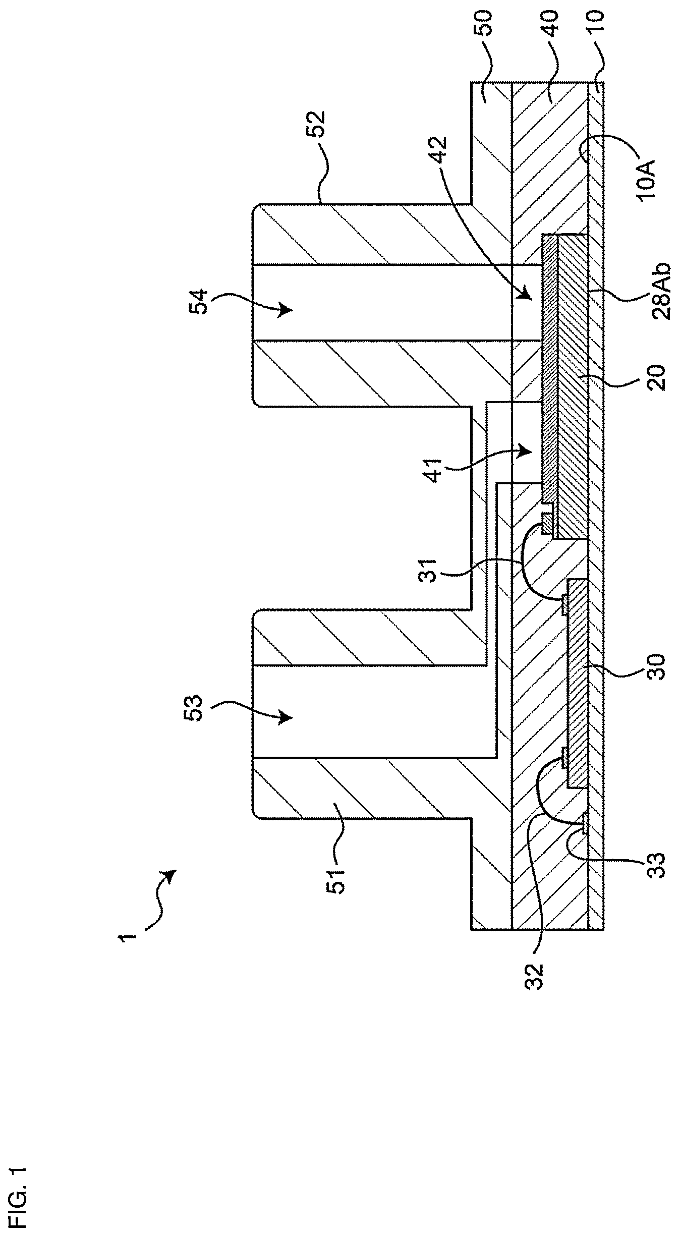
As illustrated in , a pressure sensor 1 includes a substrate 10 , a pressure sensor chip 20 , an application specific integrated circuit (ASIC) 30 , a first covering portion 40 , and a second covering portion 50 . Hereinafter, the application specific integrated circuit 30 will be referred to as an ASIC 30 . The ASIC 30 is an example of a control chip.
The substrate 10 is a plate-shaped member. The substrate 10 is made of a material such as resin, for example, epoxy resin or phenol resin, ceramic, or aluminum. A wiring pattern, a pad, a through-hole, and the like made of metal such as copper, for example, are provided on an outer surface of the substrate 10 . The wiring pattern, the pad, and the through-hole may be electrically connected to each other.
The pressure sensor chip 20 senses a minute pressure. The pressure sensor chip 20 includes two diaphragms (a first diaphragm 21 B and a second diaphragm 21 C, see and ) to be described later. The first diaphragm 21 B and the second diaphragm 21 C each sense pressure by being bent. That is, the pressure sensor 1 is capable of measuring two pressures.
The pressure sensor chip 20 is mounted on an upper surface 10 A of the substrate 10 . As a mounting method, various known methods can be used. In the first preferred embodiment, the pressure sensor chip 20 is mounted on the substrate 10 by a base portion 28 (see and ), which will be described later, being adhered to the upper surface 10 A with an adhesive.
In the first preferred embodiment, an outer shape of the pressure sensor chip 20 is a rectangular or substantially rectangular parallelepiped shape. The pressure sensor chip 20 may have a shape other than a rectangular or substantially rectangular parallelepiped shape, for example, a cylindrical or substantially cylindrical shape. The pressure sensor chip 20 is a device configured by MEMS (Micro Electro Mechanical Systems). The pressure sensor chip 20 has a structure in which a plurality of layers are stacked. A configuration of the pressure sensor chip 20 will be described in detail later.
The ASIC 30 is mounted on the upper surface 10 A of the substrate 10 . As a mounting method, various known methods can be used. In the first preferred embodiment, the ASIC 30 is adhered to the upper surface 10 A by an adhesive.
The ASIC 30 is connected to the pressure sensor chip 20 by using a plurality of conductive wires (for example, a wire 31 illustrated in ) made of, for example, aluminum or copper. The ASIC 30 is electrically connected to a plurality of pads 33 provided on the outer surface of the substrate 10 by using a plurality of conductive wires 32 made of, for example, aluminum or copper. illustrates only one wire 31 and one wire 32 , and only one pad 33 .
In the first preferred embodiment, the pressure sensor 1 includes five wires 32 . End portions of the respective five wires 32 are connected to respective pads 29 A to 29 E (see and ) to be described later. Other end portions of the respective five wires 32 are connected to the respective pads 33 .
The ASIC 30 has a function of processing a signal inputted from the pressure sensor chip 20 through the wire 31 and outputting the processed signal outside through the wire 32 . This function will be described in detail later.
The first covering portion 40 and the second covering portion 50 are made of resin such as an epoxy resin, for example.
The first covering portion 40 covers the upper surface 10 A of the substrate 10 , the pressure sensor chip 20 , the ASIC 30 , the wires 31 and 32 . The first covering portion 40 includes two cavities 41 and 42 . The cavity 41 exposes a portion of the pressure sensor chip 20 (specifically, an electrode 22 B described later) externally. The cavity 42 exposes a portion of the pressure sensor chip 20 (specifically, an electrode 22 C described later) externally.
The second covering portion 50 is joined to the first covering portion 40 . The second covering portion 50 is joined to the first covering portion 40 on an opposite side from a side where the first covering portion 40 is in contact with the pressure sensor chip 20 . The second covering portion 50 includes two cylindrical caps 51 and 52 . The caps 51 and 52 protrude away from the first covering portion 40 and the pressure sensor chip 20 . An internal space 53 of the cap 51 communicates with the cavity 41 . An internal space 54 of the cap 52 communicates with the cavity 42 .
Hereinafter, the configuration of the pressure sensor chip 20 will be described in detail. In the following description, directions of respective sides of the pressure sensor chip 20 being rectangular or substantially rectangular parallelepiped are defined as a longitudinal direction 2 , a transverse direction 3 , and a height direction 4 , respectively.
is a longitudinal sectional view of the pressure sensor chip included in the pressure sensor according to the first preferred embodiment of the present invention. is an exploded perspective view of the pressure sensor chip included in the pressure sensor according to the first preferred embodiment of the present invention. is a plan view of the pressure sensor chip included in the pressure sensor according to the first preferred embodiment of the present invention. In , the transverse direction 3 is a depth direction of a surface of paper of . As illustrated in , in the height direction 4 , a side of the base portion 28 is defined as a lower side, and a side of a second conductive layer 22 is defined as an upper side.
As illustrated in to , the pressure sensor chip 20 includes three conductive layers (a first conductive layer 21 , the second conductive layer 22 , and a third conductive layer 23 ), two insulating layers (a first insulating layer 24 and a second insulating layer 25 ), the base portion 28 , and the five pads 29 A to 29 E.
The first conductive layer 21 , the second conductive layer 22 , and the third conductive layer 23 are conductors. In the first preferred embodiment, the first conductive layer 21 , the second conductive layer 22 , and the third conductive layer 23 are made of, for example, silicon.
The first insulating layer 24 and the second insulating layer 25 are electrically insulated insulators. In the first preferred embodiment, the first insulating layer 24 and the second insulating layer 25 are made of, for example, silicon dioxide.
As illustrated in and , the base portion 28 includes a conductive layer 28 A and an insulating layer 28 B. The conductive layer 28 A is a conductor. In the first preferred embodiment, the conductive layer 28 A is made of, for example, silicon similarly to the first conductive layer 21 and the like. The insulating layer 28 B is an electrically insulated insulator. The insulating layer 28 B is made of, for example, silicon dioxide similarly to the first insulating layer 24 and the like.
As illustrated in , the conductive layer 28 A is joined to the upper surface 10 A of the substrate 10 (see ). The insulating layer 28 B is joined to an upper surface 28 Aa of the conductive layer 28 A. The third conductive layer 23 is joined to an upper surface 28 Ba of the insulating layer 28 B. The second insulating layer 25 is joined to an upper surface 23 A of the third conductive layer 23 . The first conductive layer 21 is joined to an upper surface 25 A of the second insulating layer 25 . The first insulating layer 24 is joined to an upper surface 21 A of the first conductive layer 21 . The second conductive layer 22 is joined to an upper surface 24 A of the first insulating layer 24 .
The first conductive layer 21 is sandwiched between the first insulating layer 24 and the second insulating layer 25 . The second conductive layer 22 is joined to a surface of the first insulating layer 24 on an opposite side from the first conductive layer 21 . The third conductive layer 23 is joined to a surface of the second insulating layer 25 on an opposite side from the first conductive layer 21 .
As described above, in the pressure sensor chip 20 , the base portion 28 , the third conductive layer 23 , the second insulating layer 25 , the first conductive layer 21 , the first insulating layer 24 , and the second conductive layer 22 are stacked in order from the bottom.
In the first preferred embodiment, a thickness (length in the height direction 4 ) of each of the first conductive layer 21 , the second conductive layer 22 , and the third conductive layer 23 is the same or substantially the same. In the first preferred embodiment, the first insulating layer 24 and the second insulating layer 25 have the same or substantially the same thickness. In the first preferred embodiment, the thickness of each of the first insulating layer 24 and the second insulating layer 25 is larger than the thickness of each of the first conductive layer 21 , the second conductive layer 22 , and the third conductive layer 23 .
The first conductive layer 21 , the second conductive layer 22 , and the third conductive layer 23 need not be completely the same and may be substantially the same in thickness. Further, the first conductive layer 21 , the second conductive layer 22 , and the third conductive layer 23 may have different thicknesses from each other. Further, the first insulating layer 24 and the second insulating layer 25 need not be completely the same and may be substantially the same in thickness. Further, the first insulating layer 24 and the second insulating layer 25 may have different thicknesses from each other. Further, the thickness of each of the first insulating layer 24 and the second insulating layer 25 may be equal to or less than the thickness of each of the first conductive layer 21 , the second conductive layer 22 , and the third conductive layer 23 .
As illustrated in , portions of the pressure sensor chip 20 except for a lower surface thereof (specifically, a lower surface 28 Ab of the conductive layer 28 A of the base portion 28 joined to the substrate 10 ) are covered by the first covering portion 40 .
As illustrated in and , cavities 24 B and 24 C are provided in the first insulating layer 24 . The cavity 24 B is an example of a first cavity. The cavity 24 C is an example of a second cavity. Cavities 25 B and 25 C are provided in the second insulating layer 25 . The cavity 25 B is an example of a third cavity. The cavity 25 C is an example of a fourth cavity. In the first preferred embodiment, each of the cavities 24 B, 24 C, 25 B, and 25 C has a rectangular or substantially rectangular shape in plan view when the pressure sensor chip 20 is viewed from above but may have a shape other than a rectangular or substantially rectangular shape (for example, a circular or substantially circular shape).
As illustrated in , the first conductive layer 21 includes a first diaphragm 21 B, a second diaphragm 21 C, an outer peripheral portion 21 D, communication portions 21 E and 21 F. The outer peripheral portion 21 D surrounds, in plan view, the first diaphragm 21 B, the second diaphragm 21 C, the communication portions 21 E and 21 F.
The first diaphragm 21 B and the second diaphragm 21 C are electrically connected to each other with the communication portion 21 E interposed therebetween. The first diaphragm 21 B is electrically connected to the pad 29 A with the communication portion 21 F interposed therebetween. That is, the first diaphragm 21 B, the second diaphragm 21 C, and the pad 29 A are electrically connected to each other. The pad 29 A is supported by the upper surface 25 A of the second insulating layer 25 . The pad 29 A is an example of a fifth pad. Gaps are provided between the outer peripheral portion 21 D, and the first diaphragm 21 B, the second diaphragm 21 C, and the communication portions 21 E and 21 F.
As illustrated in , the first diaphragm 21 B is sandwiched between the cavity 24 B of the first insulating layer 24 and the cavity 25 B of the second insulating layer 25 . The second diaphragm 21 C is sandwiched between the cavity 24 C of the first insulating layer 24 and the cavity 25 C of the second insulating layer 25 .
As illustrated in , in plan view, the first diaphragm 21 B and the second diaphragm 21 C have the same or substantially the same shape and area. In plan view, the first diaphragm 21 B and the second diaphragm 21 C need not be completely the same and may have substantially the same shape. In addition, in plan view, the first diaphragm 21 B and the second diaphragm 21 C need not be completely the same and may have substantially the same area. In addition, in plan view, the first diaphragm 21 B and the second diaphragm 21 C may have different shapes and/or areas.
As illustrated in , the second conductive layer 22 is located uppermost in the pressure sensor chip 20 . Thus, an upper surface 22 A of the second conductive layer 22 is exposed outside the pressure sensor chip 20 .
As illustrated in and , the second conductive layer 22 includes the electrodes 22 B and 22 C, an outer peripheral portion 22 D, and communication portions 22 E and 22 F. The outer peripheral portion 22 D surrounds, in plan view, the electrodes 22 B and 22 C and the communication portions 22 E and 22 F. The electrode 22 B is an example of a first electrode. The electrode 22 C is an example of a second electrode.
The electrode 22 B is electrically connected to a pad 29 B with the communication portion 22 E interposed therebetween. That is, the electrode 22 B and the pad 29 B are electrically connected to each other. The electrode 22 C is electrically connected to a pad 29 C with the communication portion 22 F interposed therebetween. That is, the electrode 22 C and the pad 29 C are electrically connected to each other. The pads 29 B and 29 C are supported by the upper surface 24 A of the first insulating layer 24 . The pad 29 B is an example of a first pad. The pad 29 C is an example of a second pad. Gaps are provided between the outer peripheral portion 22 D, and the electrode 22 B and the communication portion 22 E, and between the outer peripheral portion 22 D, and the electrode 22 C and the communication portion 22 F. The electrode 22 B and the communication portion 22 E are separated from the electrode 22 C and the communication portion 22 F with the outer peripheral portion 22 D interposed therebetween.
As illustrated in , the electrode 22 B faces the first diaphragm 21 B with the cavity 24 B interposed therebetween. The electrode 22 C faces the second diaphragm 21 C with the cavity 24 C interposed therebetween.
As illustrated in and , a through-hole 22 Ba is formed in the electrode 22 B. A lower end portion of the through-hole 22 Ba communicates with the cavity 24 B of the first insulating layer 24 . An upper end portion of the through-hole 22 Ba communicates with the outside of the pressure sensor chip 20 . In the first preferred embodiment, the upper end portion of the through-hole 22 Ba communicates with the cavity 41 (see ) of the first covering portion 40 . Thus, the cavity 24 B of the first insulating layer 24 communicates with an outside of the pressure sensor 1 through the through-hole 22 Ba, the cavity 41 , and the internal space 53 (see ) of the cap 51 . The through-hole 22 Ba is an example of a first communication portion.
A through-hole 22 Ca is provided in the electrode 22 C. A lower end portion of the through-hole 22 Ca communicates with the cavity 24 C of the first insulating layer 24 . An upper end portion of the through-hole 22 Ca communicates with the outside of the pressure sensor chip 20 . In the first preferred embodiment, the upper end portion of the through-hole 22 Ca communicates with the cavity 42 (see ) of the first covering portion 40 , and thus, the cavity 24 C of the first insulating layer 24 communicates with the outside of the pressure sensor 1 through the through-hole 22 Ca, the cavity 42 , and the internal space 54 (see ) of the cap 52 . The through-hole 22 Ca is an example of a second communication portion.
As illustrated in , the third conductive layer 23 includes electrodes 23 B and 23 C, an outer peripheral portion 23 D, and communication portions 23 E and 23 F. The outer peripheral portion 23 D surrounds, in plan view, the electrodes 23 B and 23 C, and the communication portions 23 E and 22 F. The electrode 23 B is an example of a third electrode. The electrode 23 C is an example of a fourth electrode.
The electrode 23 B is electrically connected to the pad 29 D with the communication portion 23 E interposed therebetween. That is, the electrode 23 B and the pad 29 D are electrically connected to each other. The electrode 23 C is electrically connected to the pad 29 E with the communication portions 23 F interposed therebetween. That is, the electrode 23 C and the pad 29 E are electrically connected to each other. The pads 29 D and 29 E are supported by the upper surface 28 Ba of the insulating layer 28 B of the base portion 28 . The pad 29 D is an example of a third pad. The pad 29 E is an example of a fourth pad. Gaps are provided between the outer peripheral portion 23 D, and the electrode 23 B and the communication portion 23 E, and between the outer peripheral portion 23 D, and the electrode 23 C and the communication portion 23 F. The electrode 23 B and the communication portion 23 E are separated from the electrode 23 C and the communication portion 23 F with the outer peripheral portion 23 D interposed therebetween.
As illustrated in , the electrode 23 B faces the first diaphragm 21 B with the cavity 25 B interposed therebetween. The electrode 23 C faces the second diaphragm 21 C with the cavity 25 C interposed therebetween.
As illustrated in , a first flow path 71 and a second flow path 72 are provided inside the pressure sensor chip 20 . Through the first flow path 71 , the cavity 24 B and the cavity 25 C communicate with each other. Through the second flow path 72 , the cavity 24 C and the cavity 25 B communicate with each other.
The first flow path 71 includes a through-hole 71 A, and spaces 71 B and 71 C. The through-hole 71 A is an example of a first through-hole. The space 71 B is an example of a first space. The space 71 C is an example of a second space.
As illustrated in , the through-hole 71 A is provided in the first conductive layer 21 . In the first preferred embodiment, the through-hole 71 A is provided between the first diaphragm 21 B and the second diaphragm 21 C.
The space 71 B is provided in the first insulating layer 24 . The space 71 B communicates with the cavity 24 B. In the first preferred embodiment, the space 71 B protrudes from the cavity 24 B in the longitudinal direction 2 . In plan view, the space 71 B overlaps the through-hole 71 A of the first conductive layer 21 . That is, the space 71 B communicates with an upper end portion of the through-hole 71 A.
The space 71 C is provided in the second insulating layer 25 . The space 71 C communicates with the cavity 25 C. In the first preferred embodiment, the space 71 C protrudes from the cavity 25 C in the longitudinal direction 2 . In plan view, the space 71 C overlaps the through-hole 71 A of the first conductive layer 21 . That is, the space 71 C communicates with a lower end portion of the through-hole 71 A.
As illustrated in , the second flow path 72 includes a through-hole 72 A, and spaces 72 B and 72 C. The through-hole 72 A is an example of a second through-hole. The space 72 B is an example of a third space. The space 72 C is an example of a fourth space.
As illustrated in , the through-hole 72 A is provided in the first conductive layer 21 . In the first preferred embodiment, the through-hole 72 A is provided between the first diaphragm 21 B and the second diaphragm 21 C. In addition, the through-hole 72 A is provided on an opposite side from the through-hole 71 A with respect to the communication portion 21 E.
The space 72 B is provided in the first insulating layer 24 . The space 72 B communicates with the cavity 24 C. In the first preferred embodiment, the space 72 B protrudes from the cavity 24 C in the longitudinal direction 2 . In plan view, the space 72 B overlaps the through-hole 72 A of the first conductive layer 21 . That is, the space 72 B communicates with an upper end portion of the through-hole 72 A.
The space 72 C is provided in the second insulating layer 25 . The space 72 C communicates with the cavity 25 B. In the first preferred embodiment, the space 72 C protrudes from the cavity 25 B in the longitudinal direction 2 . In plan view, the space 72 C overlaps the through-hole 72 A of the first conductive layer 21 . That is, the space 72 C communicates with a lower end portion of the through-hole 72 A.
The ASIC 30 is connected to the pads 29 A to 29 E of the pressure sensor chip 20 by the five wires 32 . That is, the ASIC 30 is connected to the first diaphragm 21 B and the second diaphragm 21 C with the pad 29 A interposed therebetween. Further, the ASIC 30 is connected to the electrode 22 B with the pad 29 B interposed therebetween. Further, the ASIC 30 is connected to the electrode 22 C with the pad 29 C interposed therebetween. Further, the ASIC 30 is connected to the electrode 23 B with the pad 29 D interposed therebetween. Further, the ASIC 30 is connected to the electrode 23 C with the pad 29 E interposed therebetween.
is a diagram illustrating an equivalent circuit of the pressure sensor chip of .
As illustrated in , the electrode 22 B and the first diaphragm 21 B, both of which are conductors, face each other with the cavity 24 B interposed therebetween. Thus, a capacitor C 1 (see ) is defined by the electrode 22 B and the first diaphragm 21 B. Further, the electrode 22 C and the second diaphragm 21 C, both of which are conductors, face each other with the cavity 24 C interposed therebetween. Thus, a capacitor C 2 (see ) is defined by the electrode 22 C and the second diaphragm 21 C. Further, the electrode 23 B and the first diaphragm 21 B, both of which are conductors, face each other with the cavity 25 B interposed therebetween. Thus, a capacitor C 3 (see ) is defined by the electrode 23 B and the first diaphragm 21 B. Further, the electrode 23 C and the second diaphragm 21 C, both of which are conductors, face each other with the cavity 25 C interposed therebetween. Thus, a capacitor C 4 (see ) is defined by the electrode 23 C and the second diaphragm 21 C. In the case described above, the first diaphragm 21 B and the second diaphragm 21 C define and function as electrodes of the capacitors.
is a longitudinal sectional view of the pressure sensor chip when pressure is applied to the first diaphragm 21 B and the second diaphragm 21 C. In , the above-described capacitors C 1 to C 4 are indicated by broken lines in a pseudo manner.
When the caps 51 and 52 illustrated in are each connected to different tubes or the like, fluid at different locations can be taken into the respective caps 51 and 52 . For example, it is assumed that pressure due to fluid taken into the internal space 53 of the cap 51 is a pressure P1, and pressure due to fluid taken into the internal space 54 of the cap 52 is a pressure P2.
In this case, as illustrated in , the pressure P1 reaches the cavity 24 B from the internal space 53 (see ) of the cap 51 via the cavity 41 (see ) and the through-hole 22 Ba. Further, the pressure P1 reaches the cavity 25 C from the cavity 24 B via the first flow path 71 .
On the other hand, the pressure P2 reaches the cavity 24 C from the internal space 54 (see ) of the cap 52 via the cavity 42 (see ) and the through-hole 22 Ca. Further, the pressure P2 reaches the cavity 25 B from the cavity 24 C via the second flow path 72 .
The pressure P1 reaching the cavity 24 B is applied to an upper surface 21 Ba of the first diaphragm 21 B. The pressure P2 reaching the cavity 25 B is applied to a lower surface 21 Bb of the first diaphragm 21 B. The pressure P2 reaching the cavity 24 C is applied to an upper surface 21 Ca of the second diaphragm 21 C. The pressure P1 reaching the cavity 25 C is applied to a lower surface 21 Cb of the second diaphragm 21 C. Here, when P1>P2, as illustrated in , the first diaphragm 21 B bends downward, and the second diaphragm 21 C bends upward.
In this case, since a distance between the electrodes of each of the capacitors C 1 and C 4 is increased, as compared to a state (the state illustrated in ) in which the capacitors C 1 and C 4 are not bent since the pressures P1 and P2 are not applied, capacitance values of the capacitors C 1 and C 4 are decreased as compared to the state illustrated in . On the other hand, since a distance between the electrodes of each of the capacitors C 2 and C 3 is decreased as compared to the state illustrated in , the capacitance values of the capacitors C 2 and C 3 are increased as compared to the state illustrated in .
As described above, the ASIC 30 has a function of processing a signal inputted from the pressure sensor chip 20 through the wire 31 and outputting the processed signal outside through the wire 32 . Hereinafter, the above function will be described with reference to .
is a flowchart illustrating a calculation process of calculating a differential pressure value by the ASIC. Hereinafter, the above calculation process will be described with reference to .
In steps S 10 to S 40 , the ASIC 30 calculates capacitance values Ca, Cb, Cc, and Cd of the respective capacitors C 1 , C 2 , C 3 , and C 4 . The capacitance values Ca to Cd of the respective capacitors C 1 to C 4 are calculated based on currents flowing from the capacitors C 1 to C 4 to the ASIC 30 through pads 29 A to 29 E, and voltages between the respective pads 29 E to 29 A applied to the ASIC 30 .
Specifically, the ASIC 30 calculates the capacitance value Ca of the capacitor C 1 , based on a current flowing between the pads 29 A and 29 B, and voltage applied between the pads 29 A and 29 B (S 10 ). The ASIC 30 calculates the capacitance value Cb of the capacitor C 2 , based on a current flowing between the pads 29 A and 29 C, and voltage applied between the pads 29 A and 29 C (S 20 ). The ASIC 30 calculates the capacitance value Cc of the capacitor C 3 , based on a current flowing between the pads 29 A and 29 D, and voltage applied between the pads 29 A and 29 D (S 30 ). The ASIC 30 calculates the capacitance value Cd of the capacitor C 4 , based on a current flowing between the pads 29 A and 29 E, and voltage applied between the pads 29 A and 29 E (S 40 ).
In the first preferred embodiment, the ASIC 30 includes an AD converter circuit therein, and the current values and the voltage values described above inputted to the ASIC 30 are converted from analog values to digital values in the AD converter circuit. In addition, steps S 10 to S 40 are performed in any order. Further, steps S 10 to S 40 may be performed in parallel.
Next, the ASIC 30 calculates a differential capacitance value Ctotal from the capacitance values Ca to Cd of the respective capacitors C 1 to C 4 calculated in steps S 10 to S 40 based on an equation of (Cb+Cc)−(Ca+Cd)=Ctotal (S 50 ).
Next, the ASIC 30 calculates a temperature Temp of a pressure measurement target based on an input value from a temperature sensor (not illustrated) (S 60 ). In the first preferred embodiment, the measurement target is fluid taken in from the respective caps 51 and 52 . The temperature sensor is provided to, for example, a pipe through which the fluid taken in from the caps 51 and 52 flows, or the like. The temperature sensor is connected to the ASIC 30 .
When the fluid taken in from the cap 51 is significantly different from the fluid taken in from the cap 52 in temperature, temperature sensors may be provided at both a flow position of the fluid taken in from the cap 51 and a flow position of the fluid taken in from the cap 52 . In this case, a plurality of temperatures is calculated.
Next, the ASIC 30 applies the differential capacitance value Ctotal calculated in step S 50 and the temperature Temp calculated in step S 60 to an equation of ΔP=f(Ctotal, Temp) to calculate a differential pressure value ΔP (S 70 ). The function f in the above equation corrects the differential capacitance value Ctotal in accordance with the temperature Temp, in proportion to a predetermined proportionality constant. The correction in accordance with the predetermined proportionality constant and the temperature Temp is appropriately determined based on the configuration such as a size, a material, or the like of the pressure sensor chip 20 . The calculation of the differential pressure value ΔP in step S 70 is not limited to calculation by an equation, and may be performed based on, for example, a data table of the differential pressure value ΔP with respect to each value of the differential capacitance Ctotal, or the like. The data table is stored, for example, in the ASIC 30 .
Next, the ASIC 30 outputs the differential pressure value ΔP calculated in step S 70 to an outside of the pressure sensor 1 (for example, a device connected to the pressure sensor 1 ) through the wire 32 and the substrate 10 (S 80 ).
As described above, based on signals from the electrodes 22 B, 22 C, 23 B, 23 C, the first diaphragm 21 B, and the second diaphragm 21 C, the ASIC 30 calculates the differential pressure between pressure applied to the first diaphragm 21 B and pressure applied to the second diaphragm 21 C.
The differential capacitance value Ctotal calculated by the pressure sensor 1 including the pressure sensor chip 20 described above, and a differential capacitance value Ctotal′ calculated by a pressure sensor (not illustrated) including a pressure sensor chip 120 of a comparative example were compared by simulation.
is a longitudinal sectional view of the pressure sensor chip of the comparative example.
The pressure sensor chip 120 of the comparative example includes a conductive layer 130 , a base portion 140 , and an insulating layer 150 . The conductive layer 130 and the base portion 140 are conductors. The insulating layer 150 is an electrically insulated insulator. The conductive layer 130 is joined to an upper surface 150 A of the insulating layer 150 . The base portion 140 is joined to a lower surface 150 B of the insulating layer 15 . Cavities 150 C and 150 D are provided in the insulating layer 150 . A portion of the conductive layer 130 and a portion of the base portion 140 that sandwich the cavity 150 C define a capacitor C 5 that is indicated by broken lines in in a pseudo manner. A portion of the conductive layer 130 and a portion of the base portion 140 that sandwich the cavity 150 D define a capacitor C 6 that is indicated by broken lines in in a pseudo manner. In the conductive layer 130 , the portion defining the capacitor C 5 is a first diaphragm 130 A, and the portion defining the capacitor C 6 is a second diaphragm 130 B. In , the first diaphragm 130 A and the second diaphragm 130 B are each a portion sandwiched between two broken lines.
The pressure sensor chip 120 is covered, similarly to the pressure sensor chip 20 , by a covering portion (not illustrated). Two cavities (not illustrated) are provided in the covering portion through which the conductive layer 130 of the pressure sensor chip 120 communicates externally. Through one of the two cavities, the first diaphragm 130 A communicates with an outside of the pressure sensor chip 120 . Further, the one of the two cavities communicates with the cavity 150 D of the insulating layer 150 . Through another of the two cavities, the second diaphragm 130 B communicates with the outside of the pressure sensor chip 120 . Further, the other of the two cavities communicates with the cavity 150 C of the insulating layer 150 .
In the pressure sensor chip 120 configured as described above, when the above pressure P1 is applied to an upper surface 130 Aa of the first diaphragm 130 A, and the above pressure P2 is applied to a lower surface 130 Ab of the first diaphragm 130 A, the above pressure P2 is applied to an upper surface 130 Ba of the second diaphragm 130 b , and the above pressure P1 is applied to a lower surface 130 Bb of the second diaphragm 130 B. Further, the differential capacitance value Ctotal′ of the pressure sensor chip 120 is calculated by Cb′−Ca′. Ca′ is a capacitance value of the capacitor C 5 , and Cb′ is a capacitance value of the capacitor C 6 .
is a graph showing a simulation result of the comparative example. The graph of shows the differential capacitance value Ctotal′ corresponding to a differential pressure (P2−P1) between the pressure P1 and the pressure P2 applied to the pressure sensor chip 120 . A broken line in the graph of indicates characteristics when stress is not applied. A solid line in the graph of indicates characteristics when stress is applied.
As illustrated in , as a difference between the pressure P1 and the pressure P2 increases, separation of the differential capacitance value Ctotal′ of characteristics of the solid line from the differential capacitance value Ctotal′ of characteristics of the broken line increases. That is, the fact that as the difference between the pressure P1 and the pressure P2 increases, the separation of the differential capacitance value Ctotal′ of characteristics of the solid line from the differential capacitance value Ctotal′ of the characteristics of the broken line increases indicates that as the difference between the pressure P1 and the pressure P2 increases, influence of stress received by the first diaphragm 130 A and the second diaphragm 130 B increases. The influence of the stress received by the first diaphragm 130 A and the second diaphragm 130 B results in an error in the differential capacitance value Ctotal′. That is, as the difference between the pressure P1 and the pressure P2 increases, an error of the differential capacitance value Ctotal′ of the pressure sensor chip 120 increases.
is a graph showing a simulation result of the first preferred embodiment. The graph of shows the differential capacitance value Ctotal corresponding to a differential pressure (P2−P1) between the pressure P1 and the pressure P2 applied to the pressure sensor chip 20 . A broken line in the graph of indicates characteristics when stress is not applied. A solid line in the graph of indicates characteristics when stress is applied.
As illustrated in , as the difference between the pressure P1 and the pressure P2 increases, separation of the differential capacitance value Ctotal of characteristics of the solid line from the differential capacitance value Ctotal of characteristics of the broken line increases. However, a width of the separation in is smaller than a width of the separation in . This indicates that the influence of stress received by the pressure sensor chip 20 of the first preferred embodiment is smaller than the influence of stress received by the pressure sensor chip 120 of the comparative example. As a result, an error of the differential capacitance value Ctotal of the pressure sensor chip 20 of the first preferred embodiment is smaller than an error of the differential capacitance value Ctotal′ of the pressure sensor chip 120 of the comparative example. That is, the pressure sensor chip 20 of the first preferred embodiment can detect the differential pressure between the pressure P1 and the pressure P2 with high accuracy as compared to the pressure sensor chip 120 of the comparative example.
According to the first preferred embodiment, the four capacitance values Ca, Cb, Cc, and Cd can be read by the capacitors C 1 , C 2 , C 3 , and C 4 defined by the respective cavities 24 B, 24 C, 25 B, and 25 C. By adding the capacitance values Ca and Cd of the respective cavities 24 B and 25 C communicating with each other by the first flow path 71 , it is possible to detect a capacitance value (first capacitance value) corresponding to the pressure P1 applied from outside via the through-hole 22 Ba. Similarly, by adding the capacitance values Cb and Cc of the respective cavities 24 C and 25 B communicating with each other by the second flow path 72 , it is possible to detect a capacitance value (second capacitance value) corresponding to the pressure P2 applied from outside via the through-hole 22 Ca. Based on a difference between the first capacitance value and the second capacitance value, the differential pressure between the pressure P1 and the pressure P2 can be obtained.
Pressure applied from outside to the first diaphragm 21 B of the first conductive layer 21 via the cavity 24 B is applied from above (from a side of the first insulating layer 24 ). On the other hand, pressure applied from outside to the second diaphragm 21 C of the first conductive layer 21 via the cavity 25 C is applied from below (from a side of the second insulating layer 25 ). Here, stress that is applied to the first conductive layer 21 due to warpage or the like includes a compressive stress and a tensile stress. One of the compressive stress and the tensile stress is applied to the upper surface of the first conductive layer 21 , and another of the compressive stress and the tensile stress is applied to the lower surface of the first conductive layer 21 . Thus, the capacitance value Ca of the cavity 24 B is influenced by the one of the compressive stress and the tensile stress, and the capacitance value Cd of the cavity 25 C is influenced by the other of the compressive stress and the tensile stress. Thus, when the capacitance value Ca of the cavity 24 B and the capacitance value Cd of the cavity 25 C are added, at least a portion of the stress (the compressive stress and the tensile stress) influencing the respective capacitance values is cancelled.
Also, for the cavities 24 C and 25 B, similarly to the cavities 24 B and 25 C, the capacitance value Cb of the cavity 24 C is influenced by one of the compressive stress and the tensile stress, and the capacitance value Cc of the cavity 25 B is influenced by another of the compressive stress and the tensile stress. Thus, when the capacitance value Cb of the cavity 24 C and the capacitance value Cc of the cavity 25 B are added, at least a portion of the stress (the compressive stress and the tensile stress) influencing the respective capacitance values is canceled.
As a result, since the influence of the stress applied to the first conductive layer 21 can be reduced, an error of a detected capacitance value can be reduced.
According to the first preferred embodiment, in plan view, the first diaphragm 21 B and the second diaphragm 21 C have the same or substantially the same area. Further, the thickness of the first insulating layer 24 and the thickness of the second insulating layer 25 are the same or substantially the same. Accordingly, variations in the influence of the stress affecting the capacitance values Ca, Cb, Cc, and Cd of the respective cavities 24 B, 24 C, 25 B, and 25 C are reduced. Thus, it is possible to increase an amount of cancellation of the stress.
According to the first preferred embodiment, it is possible to detect the capacitance values Ca, Cb, Cc, and Cd of the respective cavities 24 B, 24 C, 25 B, and 25 C, based on values of currents flowing through the respective pads 29 A to 29 E and values of voltages applied between the pads.
According to the first preferred embodiment, the first flow path 71 and the second flow path 72 can be provided simply by providing the through-hole in the first conductive layer 21 and providing the space in each of the first insulating layer 24 and the second insulating layer 25 . That is, the first flow path 71 and the second flow path 72 can be provided without requiring a complicated configuration or a complicated manufacturing process.
According to the first preferred embodiment, the cavities 24 B and 24 C can be made to communicate with the outside of the pressure sensor chip 20 only by providing the through-hole in the second conductive layer 22 , that is, without requiring a complicated configuration.
According to the first preferred embodiment, in the pressure sensor 1 including the pressure sensor chip 20 , it is possible to cancel at least a portion of the stress (the compressive stress and the tensile stress) influencing each of them.
In the first preferred embodiment, of the cavities 24 B and 25 C communicating with each other, the cavity 24 B communicates with the outside of the pressure sensor chip 20 . In addition, in the first preferred embodiment, of the cavities 24 C and 25 B communicating with each other, the cavity 24 C communicates with the outside of the pressure sensor chip 20 . That is, in the first preferred embodiment, the cavities 24 B and 24 C provided in the first insulating layer 24 communicate with the outside of the pressure sensor chip 20 .
However, the cavities 25 B and 25 C provided in the second insulating layer 25 may communicate with the outside of the pressure sensor chip 20 . In this case, a flow path through which the cavity 25 B communicates with the outside of the pressure sensor chip 20 , and a flow path through which the cavity 25 C communicates with the outside of the pressure sensor chip 20 are provided in the pressure sensor chip 20 . For example, the above flow paths extend from the respective cavities 25 B and 25 C, to the outside of the pressure sensor chip 20 , through the second insulating layer 25 , the first conductive layer 21 , the first insulating layer 24 , and the second conductive layer 22 . In the case of the above example, the flow path through which the cavity 25 C and the outside of the pressure sensor chip 20 communicate with each other corresponds to the first communication portion. In addition, the flow path through which the cavity 25 B and the outside of the pressure sensor chip 20 communicate with each other corresponds to the second communication portion.
Further, both of the cavities 24 B and 25 C may communicate with the outside of the pressure sensor chip 20 , or both of the cavities 24 C and 25 B may communicate with the outside of the pressure sensor chip 20 .
In the first preferred embodiment, the cavity 24 B and the cavity 25 C communicate with each other through the first flow path 71 as illustrated in and , and the cavity 24 C and the cavity 25 B communicate with each other through the second flow path 72 as illustrated in and . However, it is not limited to the first flow path 71 and the second flow path 72 as illustrated in and that make the cavities 24 B and 25 C communicate with each other and the cavities 24 C and 25 B communicate with each other.
For example, the flow path through which the cavities 24 B and 25 C communicate with each other, and the flow path through which the cavities 24 C and 25 B communicate with each other may pass through the base portion 28 .
Further, for example, the flow path through which the cavities 24 B and 25 C communicate with each other, and the flow path through which the cavities 24 C and 25 B communicate with each other may pass through the outside of the pressure sensor chip 20 . In this case, each of the cavities 24 B, 24 C, 25 B, and 25 C communicates with the outside of the pressure sensor chip 20 by a through-hole or the like, and two through-holes corresponding to the cavities 24 B and 25 C are connected to each other by a pipe or the like. Further, two through-holes corresponding to the cavities 24 C and 25 B are connected to each other by a pipe or the like.
Second Preferred Embodiment
In the first preferred embodiment, the pressure sensor chip 20 includes the five pads 29 A to 29 E. The pad 29 A is electrically connected to the first diaphragm 21 B and the second diaphragm 21 C. The pads 29 B, 29 C, 29 D, and 29 E are electrically connected to the electrodes 22 B, 22 C, 23 B, and 23 C, respectively. However, the number of pads included in the pressure sensor chip 20 is not limited to five. Further, a combination of connection between the respective pads and the first diaphragm 21 B, the second diaphragm 21 C, and the electrodes 22 B, 22 C, 23 B, and 23 C is not limited to the combination of connection described in the first preferred embodiment.
is an exploded perspective view of a pressure sensor chip included in a pressure sensor according to a second preferred embodiment of the present invention. A pressure sensor chip 200 of the pressure sensor according to the second preferred embodiment differs from the pressure sensor chip 20 of the pressure sensor 1 according to the first preferred embodiment in that the pressure sensor chip 200 includes four pads 129 A to 129 D.
As illustrated in , the pressure sensor chip 200 includes the pads 129 A to 129 D instead of the pads 29 A to 29 E.
The pad 129 A is electrically connected to the first diaphragm 21 B. The pad 129 B is electrically connected to the second diaphragm 21 C. The first diaphragm 21 B and the second diaphragm 21 C are not electrically connected to each other. The pads 129 A and 129 B are supported by the upper surface 25 A of the second insulating layer 25 . The pad 129 A is an example of a third pad. The pad 129 B is an example of a fourth pad.
The pad 129 C is electrically connected to the electrode 22 B. The pad 129 D is electrically connected to the electrode 22 C. The pads 129 C and 129 D are supported by the upper surface 24 A of the first insulating layer 24 .
The pressure sensor chip 200 includes vias 81 and 82 . Both of the vias 81 and 82 are through-holes passing through the first insulating layer 24 , the first conductive layer 21 , and the second insulating layer 25 . The vias 81 and 82 are filled with conductors. An upper end portion of the via 81 is connected to the electrode 22 B. A lower end portion of the via 81 is connected to the electrode 23 C. Thus, the electrodes 22 B and 23 C are electrically connected to each other through the via 81 . An upper end portion of the via 82 is connected to the electrode 22 C. A lower end portion of the via 82 is connected to the electrode 23 B. Thus, the electrodes 22 C and 23 B are electrically connected to each other through the via 82 .
As described above, the pad 129 C is electrically connected to the electrodes 22 B and 23 C. The pad 129 C is an example of a first pad. The pad 129 D is electrically connected to the electrodes 22 C and 23 B. The pad 129 D is an example of a second pad.
is a diagram illustrating an equivalent circuit of the pressure sensor chip of . Also, in the case of the second preferred embodiment, similarly to the case of the first preferred embodiment, the differential capacitance value Ctotal can be calculated from the capacitance values of the respective capacitors C 1 to C 4 , based on the equation (Cb+Cc)−(Ca+Cd)=Ctotal. Further, a simulation result is similar to that in the first preferred embodiment. That is, the pressure sensor chip 200 of the second preferred embodiment can detect a differential pressure between the pressure P1 and the pressure P2 with high accuracy as compared to the pressure sensor chip 120 of the comparative example.
According to the second preferred embodiment, it is possible to detect the capacitance values Ca, Cb, Cc, and Cd of the respective cavities 24 B, 24 C, 25 B, and 25 C, based on values of currents flowing through the respective pads 129 A to 129 D and values of voltage applied between the pads. Further, according to the second preferred embodiment, since one pad is connected to two electrodes, it is possible to reduce the number of electrodes, as compared to the first preferred embodiment in which one pad is connected to one electrode.
Third Preferred Embodiment
is a longitudinal sectional view of a pressure sensor chip included in a pressure sensor according to a third preferred embodiment of the present invention. A pressure sensor chip 300 of the pressure sensor according to the third preferred embodiment is different from the pressure sensor chip 20 of the pressure sensor 1 according to the first preferred embodiment in that a base portion 90 is included. In other words, the pressure sensor chip 300 includes the two base portions 28 and 90 .
As illustrated in , the base portion 28 is joined to the third conductive layer 23 on an opposite side from the second insulating layer 25 . The base portion 90 is joined to the second conductive layer 22 on an opposite side from the first insulating layer 24 . In the third preferred embodiment, the base portion 90 is an example of a first base portion, and the base portion 28 is an example of a second base portion.
The base portion 90 includes a conductive layer 90 A and an insulating layer 90 B. In the third preferred embodiment, the conductive layer 90 A is made of, for example, silicon similarly to the conductive layer 28 A of the base portion 28 , and the insulating layer 90 B is made of, for example silicon dioxide similarly to the insulating layer 28 B of the base portion 28 .
The insulating layer 90 B is joined to the upper surface 22 A of the second conductive layer 22 . The conductive layer 90 A is joined to an upper surface 90 Ba of the insulating layer 90 B.
A configuration of the conductive layer 90 A is the same as or similar to the configuration of the conductive layer 28 A of the base portion 28 . A configuration of the insulating layer 90 B is the same as or similar to the configuration of the insulating layer 28 B of the base portion 28 . For example, thicknesses of the conductive layer 90 A and the insulating layer 90 B are the same or substantially the same as thicknesses of the conductive layer 28 A and the insulating layer 28 B, respectively.
As described above, the base portions 28 and 90 are configured to be symmetrical or substantially symmetrical to each other with respect to the first conductive layer 21 .
According to the third preferred embodiment, the pressure sensor chip 300 is configured to be symmetrical or substantially symmetrical in a stacking direction (the height direction 4 ) of the respective layers. Thus, warpage of the pressure sensor chip 300 can be reduced or prevented. As a result, generation of stress in the first conductive layer 21 can be reduced or prevented.
According to the third preferred embodiment, the respective layers (the first conductive layer 21 , the second conductive layer 22 , the third conductive layer 23 , the first insulating layer 24 , and the second insulating layer 25 ) can be shielded by the base portions 28 and 90 including the conductive layers 28 A and 90 A. Accordingly, since noise to each layer can be reduced, accuracy of the detected capacitance values Ca, Cb, Cc, and Cd is improved.
In the third preferred embodiment, each of the base portions 28 and 90 includes, for example, the two layers, but each of the base portions 28 and 90 only needs to include at least one layer. For example, each of the base portions 28 and 90 may include two insulating layers and three conductive layers.
In the third preferred embodiment, each of the base portions 28 and 90 includes the conductive layer, but only one of the base portions 28 and 90 may include the conductive layer, and another of the base portions 28 and 90 may include only the insulating layer without including the conductive layer. In addition, each of the base portions 28 and 90 may include only the insulating layer without including the conductive layer.
In the third preferred embodiment, the base portions 28 and 90 each include the same number of layers, but the number of layers of the base portion 28 and the number of layers of the base portion 90 may be different from each other. Further, in the third preferred embodiment, the base portions 28 and 90 have the same or substantially the same configuration, but the base portions 28 and 90 may have configurations different from each other. For example, the base portion 28 may include only one insulating layer, and the base portion 90 may include two conductive layers.
By appropriately combining any preferred embodiments among the various preferred embodiments described above, it is possible to achieve the advantageous effects of the respective preferred embodiments.
While preferred embodiments of the present invention have been described above, it is to be understood that variations and modifications will be apparent to those skilled in the art without departing from the scope and spirit of the present invention. The scope of the present invention, therefore, is to be determined solely by the following claims.
Figures (13)
Citations
This patent cites (15)
- US6374680
- US9726561
- US11299392
- US11540048
- US11733114
- US11767218
- US11827511
- US2010/0199778
- US2017/0315008
- US2018/0074090
- US2022/0048761
- US2001013026
- US2010538242
- US2020053485
- US6201419