Abstract
According to one embodiment, a sensor includes a base, first and second detection element portions, first to third resistor terminals, and first and second conductive terminals. The base includes first and second base regions. The first detection element portion is provided at the first base region. The first detection element portion includes a first detection dement. The first detection dement includes a first resistance member and a first conductive member. The first resistance member includes a first resistance portion and other portion. The first conductive member includes a first conductive portion and other portion. The second detection element portion is provided at the second base region. The second detection dement portion includes a second detection element. The second detection element includes a second resistance member and a second conductive member. The second resistance member includes a second resistance portion and other portion. The second conductive member includes a second conductive portion and other portion.
Claims (20)
1. A sensor, comprising: a base including a first base region and a second base region, a first detection element portion provided at the first base region, the first detection element portion including a first detection element, the first detection element including a first resistance member and a first conductive member, the first resistance member including a first resistance portion and a first resistance other portion, the first conductive member including a first conductive portion and a first conductive other portion; a second detection element portion provided at the second base region, the second detection element portion including a second detection element, the second detection element including a second resistance member and a second conductive member, the second resistance member including a second resistance portion and a second resistance other portion, the second conductive member including a second conductive portion and a second conductive other portion; a first resistor terminal electrically connected with the first resistance portion; a second resistor terminal electrically connected with the first resistance other portion and the second resistance portion; a third resistor terminal electrically connected with the second resistance other portion; a first conductive terminal electrically connected with the first conductive portion; and a second conductive terminal electrically connected with the first conductive other portion.
4. A sensor, comprising: a base including a first base region and a second base region, a first detection element portion provided at the first base region, the first detection element portion including a first detection element, the first detection element including a first resistance member and a first conductive member, the first resistance member including a first resistance portion and a first resistance other portion, the first conductive member including a first conductive portion and a first conductive other portion; a second detection element portion provided at the second base region, the second detection element portion including a second detection element, the second detection element including a second resistance member and a second conductive member, the second resistance member including a second resistance portion and a second resistance other portion, the second conductive member including a second conductive portion and a second conductive other portion; a first resistor terminal electrically connected with the first resistance portion; a second resistor terminal electrically connected with the first resistance other portion; a third resistor terminal electrically connected with the second resistance other portion; a fourth resistor terminal electrically connected with the second resistance portion; a first conductive terminal electrically connected with the first conductive portion; and a second conductive terminal electrically connected with the first conductive other portion.
Show 18 dependent claims
2. The sensor according to claim 1 , further comprising a connecting conductive member provided on the base, the connecting conductive member electrically connecting the first resistance other portion and the second resistance portion.
3. The sensor according to claim 1 , further comprising a processor electrically connected with the first resistor terminal, the second resistor terminal, the third resistor terminal, the first conductive terminal, and the second conductive terminal, the processor being configured to perform a first operation of supplying a first current between the first conductive terminal and the second conductive terminal to raise the temperature of the first detection element, in the first operation, the processor being configured to output a signal corresponding to a first ratio of a first electric resistance between the first resistor terminal and the second resistor terminal to a second electric resistance between the second resistor terminal and the third resistor terminal.
5. The sensor according to claim 4 , further comprising a processor electrically connected with the first resistor terminal, the second resistor terminal, the third resistor terminal, the fourth resistor terminal, the first conductive terminal, and the second conductive terminal, the processor being configured to perform a first operation of supplying a first current between the first conductive terminal and the second conductive terminal to raise the temperature of the first detection element, in the first operation, the processor being configured to output a signal corresponding to a first ratio of a first electric resistance between the first resistor terminal and the second resistor terminal to a second electric resistance between the third resistor terminal and the fourth resistor terminal.
6. The sensor according to claim 3 , wherein the first ratio changes according to a concentration of a first element included in an atmosphere around the first detection element and the second detection element.
7. The sensor according to claim 3 , wherein the first electric resistance of the first detection element when the temperature rises changes according to a concentration of a first element included in the atmosphere around the first detection element.
8. The sensor according to claim 6 , wherein the first element includes at least one selected from the group consisting of hydrogen, helium, carbon dioxide, methane and sulfur hexafluoride.
9. The sensor according to claim 5 , further comprising: a third conductive terminal electrically connected with the second conductive portion; and a fourth conductive terminal electrically connected with the second conductive other portion, the processor is configured to perform a second operation switching from the first operation, the second operation including supplying a second current between the third conductive terminal and the fourth conductive terminal to raise a temperature of the second detection element, in the second operation, the processor s configured to output a signal corresponding to a second ratio of a third electric resistance between the first resistor terminal and the second resistor terminal to a fourth electric resistance between the second resistor terminal and the third resistor terminal.
10. The sensor according to claim 9 , wherein the processor is configured to output an average of the first ratio and the second ratio.
11. The sensor according to claim 1 , wherein at least one of the second conductive portion or the second conductive other portion has a floating potential or a fixed potential.
12. The sensor according to claim 1 , wherein the second conductive member is a dummy conductive member.
13. The sensor according to claim 1 , wherein the first detection element portion further includes a first connection portion and a first support portion, the first support portion is fixed to the base, a part of the first connection portion is supported by the first support portion, an other part of the first connection portion supports the first detection element to be apart from the first base region, the second detection element portion further includes a second connection portion and a second support portion, the second support portion is fixed to the base, a part of the second connection portion is supported by the second support portion, and an other part of the second connection portion supports the second detection element to be apart from the second base region.
14. The sensor according to claim 13 , wherein a first gap is provided between the first base region and the first detection element, and a second gap is provided between the second base region and the second detection element.
15. The sensor according to claim 13 , wherein the first detection element portion further includes a first other connection portion and a first other support portion, the first other support portion is fixed to the base, a part of the first other connection portion is supported by the first other support portion, an other part of the first other connection portion supports the first detection element to be apart from the first base region, the second detection element portion further includes a second other connection portion and a second other support portion, the second other support portion is fixed to the base, a part of the second other connection portion is supported by the second other support portion, an other part of the second other connection portion supports the second detection element to be apart from the second base region, at least a part of the first detection element is located between the first connection portion and the first other connection portion, and at least a part of the second detection element is located between the second connection portion and the second other connection portion.
16. The sensor according to claim 15 , wherein the first detection element portion further includes a first conductive layer, at least a part of the first conductive layer is provided at the first support portion, a current flowing between the first resistor terminal and the first resistance portion flows through the first conductive layer, the second detection element portion further includes a second conductive layer, at least a part of the second conductive layer is provided at the second support portion, and a current flowing between the second resistor terminal and the second resistance portion flows through the second conductive layer.
17. The sensor according to claim 16 , wherein the first detection element portion further includes a third conductive layer, at least a part of the third conductive layer is provided at the first support portion, and a first current flowing between the first conductive terminal and the first conductive portion flows through the third conductive layer.
18. The sensor according to claim 17 , wherein the second detection element portion further includes a fourth conductive layer, at least a part of the fourth conductive layer is provided at the second support portion, and the fourth conductive layer is electrically connected with the second conductive portion.
19. The sensor according to claim 16 , wherein the first detection element portion further includes a third connection portion, a third support portion, and a third conductive layer, the third support portion is fixed to the base, a part of the third connection portion is supported by the third support portion, an other part of the third connection portion supports the first detection element to be apart from the first base region, at least a part of the third conductive layer is provided at the third support portion, and a first current flowing between the first conductive terminal and the first conductive portion flows through the third conductive layer.
20. The sensor according to claim 19 , wherein the second detection element portion further includes a fourth connection portion, a fourth support portion, and a fourth conductive layer, the fourth support portion is fixed to the base, a part of the fourth connection portion is supported by the fourth support portion, an other part of the fourth connection portion supports the second detection element to be apart from the second base region, at least a part of the fourth conductive layer is provided at the fourth support portion, and the fourth conductive layer is electrically connected with the second conductive portion.
Full Description
Show full text →
CROSS-REFERENCE TO RELATED APPLICATIONS
This application is based upon and claims the benefit of priority from Japanese Patent Application No. 2021-096291, filed on Jun. 9, 2021; the entire contents of which are incorporated herein by reference.
FIELD
Embodiments described herein relate generally to a sensor.
BACKGROUND
For example, there is a sensor that uses a MEMS (Micro Electro Mechanical Systems) element or the like. It is desirable to improve the characteristics of the sensor.
BRIEF DESCRIPTION OF THE DRAWINGS
is a schematic cross-sectional view illustrating a sensor according to a first embodiment;
A and B are schematic cross-sectional views illustrating the sensor according to the first embodiment;
is a schematic plan view illustrating the sensor according to the first embodiment;
A and B are schematic plan views illustrating the sensor according to the first embodiment;
is a schematic plan view illustrating a sensor according to the first embodiment;
is a schematic plan view illustrating a sensor according to a second embodiment; and
is a schematic plan view illustrating a sensor according to a third embodiment.
DETAILED DESCRIPTION
According to one embodiment, a sensor includes a base, a first detection element portion, a second detection element portion, a first resistor terminal, a second resistor terminal, a third resistor terminal, a first conductive terminal, and a second conductive terminal. The base includes a first base region and a second base region. The first detection element portion is provided at the first base region. The first detection element portion includes a first detection element. The first detection element includes a first resistance member and a first conductive member. The first resistance member includes a first resistance portion and a first resistance other portion. The first conductive member includes a first conductive portion and a first conductive other portion. The second detection element portion is provided at the second base region. The second detection element portion includes a second detection element. The second detection element includes a second resistance member and a second conductive member. The second resistance member includes a second resistance portion and a second resistance other portion. The second conductive member includes a second conductive portion and a second conductive other portion. The first resistor terminal is electrically connected with the first resistance portion. The second resistor terminal is electrically connected with the first resistance other portion and the second resistance portion. The third resistor terminal is electrically connected with the second resistance other portion. The first conductive terminal is electrically connected with the first conductive portion. The second conductive terminal is electrically connected with the first conductive other portion.
According to one embodiment, a sensor includes a base, a first detection element portion, a second detection element portion, a first resistor terminal, a second resistor terminal, a third resistor terminal, a fourth resistor terminal, a first conductive terminal, and a second conductive terminal. The base includes a first base region and a second base region. The first detection element portion is provided at the first base region. The first detection element portion includes a first detection element. The first detection element includes a first resistance member and a first conductive member. The first resistance member includes a first resistance portion and a first resistance other portion. The first conductive member includes a first conductive portion and a first conductive other portion. The second detection element portion is provided at the second base region. The second detection element portion includes a second detection element. The second detection element includes a second resistance member and a second conductive member. The second resistance member includes a second resistance portion and a second resistance other portion. The second conductive member includes a second conductive portion and a second conductive other portion. The first resistor terminal is electrically connected with the first resistance portion. The second resistor terminal is electrically connected with the first resistance other portion. The third resistor terminal is electrically connected with the second resistance other portion. The fourth resistor terminal is electrically connected with the second resistance portion. The first conductive terminal is electrically connected with the first conductive portion. The second conductive terminal is electrically connected with the first conductive other portion.
Various embodiments are described below with reference to the accompanying drawings.
The drawings are schematic and conceptual; and the relationships between the thickness and width of portions, the proportions of sizes among portions, etc., are not necessarily the same as the actual values. The dimensions and proportions may be illustrated differently among drawings, even for identical portions.
In the specification and drawings, components similar to those described previously or illustrated in an antecedent drawing are marked with like reference numerals, and a detailed description is omitted as appropriate.
First Embodiment
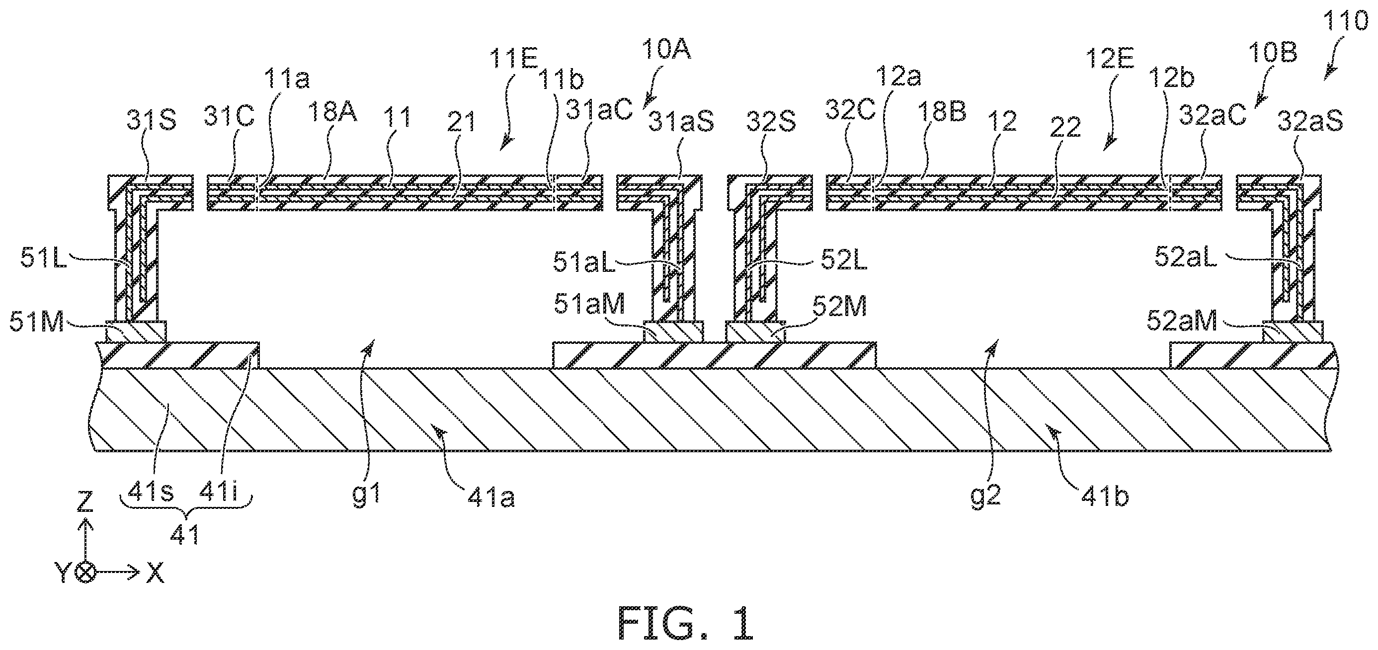
is a schematic cross-sectional view illustrating a sensor according to a first embodiment.
A and B are schematic cross-sectional views illustrating the sensor according to the first embodiment.
is a schematic plan view illustrating the sensor according to the first embodiment,
is a cross-sectional view taken along the line A 1 -A 2 of . A is a cross-sectional view taken along the line B 1 -B 2 of . B is a cross-sectional view taken along the line C 1 -C 2 of .
As shown in , 2 A, 2 B and 3 , a sensor 110 according to the embodiment includes a base 41 , a first detection element portion 10 A, a second detection element portion 10 B, a first resistor terminal 51 , a second resistor terminal 52 , a third resistor terminal 53 , a first conductive terminal 61 , and a second conductive terminal 62 .
The base 41 includes a first base region 41 a and a second base region 41 b . In this example, the base 41 includes a substrate 41 s and an insulating film 41 i . The substrate 41 s may be, for example, a semiconductor substrate (for example, a silicon substrate), The substrate 41 s may include, for example, a semiconductor circuit or the like. The substrate 41 s may include a connecting member such as a via electrode.
The first detection element portion 10 A is provided at the first base region 41 a . A direction from the first base region 41 a to the first detection element portion 10 A is a Z-axis direction. One direction perpendicular to the Z-axis direction is defined as an X-axis direction. The direction perpendicular to the Z-axis direction and the X-axis direction is defined as a Y-axis direction.
The first detection element portion 10 A includes a first detection element 11 E, The first detection element 11 E includes a first resistance member 11 and a first conductive member 21 . As shown in , the first resistance member 11 includes a first resistance portion 11 a and a first resistance other portion 11 b . For example, the first resistance portion 11 a may be one end of the first resistance member 11 , The first resistance other portion 11 b may be another end portion of the first resistance member 11 . As shown in A and 3 , the first conductive member 21 includes a first conductive portion 21 a and a first conductive other portion 21 b . For example, the first conductive portion 21 a may be one end of the first conductive member 21 . The first conductive other portion 21 b may be another end of the first conductive member 21 .
As shown in , in this example, the first detection element portion 10 A further includes a first connection portion 31 C and a first support portion 31 S. The first support portion 31 S is fixed to the base 41 . A part of the first connection portion 31 C is supported by the first support portion 31 S, Another part of the first connection portion 31 C supports the first detection element 11 E to be apart from the first base region 41 a . A first gap g 1 is provided between the first base region 41 a and the first detection element 11 E.
In this example, the first detection element portion 10 A further includes a first other connection portion 31 a C and a first other support portion 31 a S. The first other support portion 31 a S is fixed to the base 41 . A part of the first other connection portion 31 a C is supported by the first other support portion 31 a S. Another part of the first other connection portion 31 a C supports the first detection element 11 E to be apart from the first base region 41 a . In this example, at least a part of the first detection element 11 E is located between the first connection portion 31 C and the first other connection portion 31 a C.
The second detection element portion 103 is provided at the second base region 41 b . A direction from the second base region 41 b to the second detection element portion 10 B is along the Z-axis direction.
The second detection element portion 103 includes a second detection element 12 E. The second detection element 12 E includes a second resistance member 12 and a second conductive member 22 . As shown in , the second resistance member 12 includes a second resistance portion 12 a and a second resistance other portion 12 b . For example, the second resistance portion 12 a may be one end of the second resistance member 12 . The second resistance other portion 12 b may be another end portion of the second resistance member 12 , As shown in B and 3 , the second conductive member 22 includes a second conductive portion 22 a and a second conductive other portion 22 b . For example, the second conductive portion 22 a may be one end of the second conductive member 22 . The second conductive other portion 22 b may be another end of the second conductive member 22 .
As shown in , in this example, the second detection element portion 10 B further includes a second connection portion 32 C and a second support portion 32 S. The second support portion 32 S is fixed to the base 41 , A part of the second connection portion 32 C is supported by the second support portion 32 S. Another part of the second connection portion 32 C supports the second detection element 12 E to be apart from the second base region 41 b . A second gap g 2 is provided between the second base region 41 b and the second detection element 12 E.
In this example, the second detection element portion 10 B further includes a second other connection portion 32 a C and a second other support portion 32 a S. The second other support portion 32 a S is fixed to the base 41 . A part of the second other connection portion 32 a C is supported by the second other support portion 32 a S, Another part of the second other connection portion 32 a C supports the second detection element 12 E to be apart from the second base region 41 b . In this example, at least a part of the second detection element 12 E is between the second connection portion 32 C and the second other connection portion 32 a C.
By supporting the first detection element 11 E and the second detection element 12 E apart from the base 41 , it is possible to suppress the heat of these detection elements from being conducted through the base 41 , This facilitates stable detection of the detection target with high sensitivity.
The first resistor terminal 51 is electrically connected with the first resistance portion 11 a . In this example, the second resistor terminal 52 is electrically connected with the first resistance other portion lib and the second resistance portion 12 a . The third resistor terminal 53 is electrically connected with the second resistor other portion 12 b . As will be described later, other resistor terminals may be provided. In this case, the second resistor terminal 52 may be electrically connected with the first resistance other portion lib, and the other resistor terminal may be electrically connected with the second resistance portion 12 a.
In this example, as shown in , the connecting conductive member 25 is provided. The connecting conductive member 25 is provided on the base 41 , The connecting conductive member 25 electrically connects the first resistance other portion 11 b and the second resistance portion 12 a . In this example, the second resistor terminal 52 is electrically connected with the first resistance other portion lib and the second resistance portion 12 a via the connecting conductive member 25 .
The first conductive terminal 61 is electrically connected with the first conductive portion 21 a , The second conductive terminal 62 is electrically connected with the first conductive other portion 21 b.
As shown in , a processor 70 may be provided in the sensor 110 . The processor 70 may be included in the sensor 110 . The processor 70 may be provided separately from the sensor 110 , The processor 70 is electrically connected with the first resistor terminal 51 , the second resistor terminal 52 , the third resistor terminal 53 , the first conductive terminal 61 , and the second conductive terminal 62 .
The processor 70 can perform a first operation. In the first operation, the processor 70 supplies the first current i 1 between the first conductive terminal 61 and the second conductive terminal 62 to raise the temperature of the first detection element 11 E, A first current i 1 flows through the first conductive member 21 . Due to Joule heat, the temperature of the first conductive member 21 rises with respect to the atmospheric temperature, and the temperature of the first detection element 11 E rises. The first current i 1 may be alternating current or direct current.
In the first operation, the processor 70 can output a signal 70 s corresponding to a first ratio of a first electric resistance between a first resistor terminal 51 and the second resistor terminal 52 to a second electric resistance between the second resistor terminal 52 and the third resistor terminal 53 . “Corresponding to the first ratio” includes “corresponding to the reciprocal of the first ratio”.
For example, the electric resistance of the first resistance member 11 changes according to the temperature of the first resistance member 11 . The temperature of the first resistance member 11 is substantially the same as the temperature of the first detection element 11 E. For example, the electric resistance of the second resistance member 12 changes according to the temperature of the second resistance member 12 . The temperature of the second resistance member 12 is substantially the same as the temperature of the second detection element 12 E. As described above, in the first operation, for example, the temperature of the first detection element 11 E rises, and the temperature of the first resistance member 11 also rises. On the other hand, the processor 70 does not supply a current to the second conductive member 22 in, for example, the first operation. In the first operation, no current flows through the second conductive member 22 , and the temperatures of the second detection element 12 E and the second resistance member 12 do not substantially change. The first resistance member 11 and the second resistance member 12 become, for example, at least a part of a half-bridge circuit. The first ratio of the first electric resistance to the second electric resistance depends on the temperature difference between the two resistance members.
Here, the first ratio when a first element to be inspected exists in the atmosphere around the first detection element 11 E changes from the first ratio when the atmosphere does not include the first element. This is based on the fact that the temperature conduction characteristics of the first detection element 11 E change depending on the presence (and concentration) of the first element. For example, the first element includes at least one selected from the group consisting of hydrogen, helium, carbon dioxide, methane and sulfur hexafluoride (SF6). When the atmosphere includes hydrogen as the first element, the temperature of the first detection element 11 E is lower than when the atmosphere includes substantially no hydrogen. The first ratio changes according to the concentration of the first element included in the atmosphere around the first detection element and the second detection element.
By utilizing such characteristics, the sensor 110 can detect the first element. The first ratio changes according to the concentration of the first element included in the atmosphere around the first detection element 11 E and the second detection element 12 E, For example, the first electric resistance when the temperature of the first detection element 11 E rises changes according to the concentration of the first element included in the atmosphere around the first detection element 11 E, For example, the processor 70 can detect the presence/absence or concentration of the first element to be detected by detecting the first ratio.
In the embodiment, a plurality of detection element portions are provided on one base 41 . The second detection element portion 103 E has substantially the same structure as the first detection element portion 10 A. As a result, the heat capacity of the second detection element portion 10 B becomes the same as the heat capacity of the first detection element portion 10 A. In the embodiment, by detecting the ratio of the electric resistances of these two detection element portions, it is possible to detect with higher accuracy and higher sensitivity.
For example, even when the ambient temperature of the sensor 110 changes, the influence of the change in the ambient temperature can be suppressed by using the two detection element portions. In the embodiment, the change in the electric resistance of the first detecting element 11 E due to the presence or absence or the concentration of the first element is detected by suppressing other influences. It is possible to provide a sensor whose characteristics can be improved.
In the embodiment, the second detection element portion 10 B has substantially the same structure as the first detection element portion 10 A. The length, width, thickness and material of the second resistance member 12 are substantially the same as the length, width, thickness and material of the first resistance member 11 . The length, width, thickness and material of the second conductive member 22 are substantially the same as the length, width, thickness and material of the first conductive member 21 .
In the embodiment, the second conductive member 22 does not have to be supplied with an electric current. For example, at least one of the second conductive portion 22 a and the second conductive other portion 22 b may have a floating potential. For example, the second conductive member 22 is a dummy conductive member. The potential of the second conductive member 22 may be a fixed potential (for example, a ground potential).
As shown in , the first detection element portion 10 A (and the first detection element 11 E) may include the first insulating portion 18 A. The second detection element portion 10 B (and the second detection element 12 E) may include the second insulating portion 18 B, At least a part of the first insulating portion 18 A is provided around the first resistance member 11 and the first conductive member 21 . A part of the first insulating portion 18 A is provided between the first resistance member 11 and the first conductive member 21 . At least a part of the second insulating portion 18 B is provided around the second resistance member 12 and the second conductive member 22 . A part of the second insulating portion 18 B is provided between the second resistance member 12 and the second conductive member 22 . The second insulating portion 18 B has substantially the same structure as the first insulating portion 18 A. The length, width, thickness and material of the second insulating portion 188 are substantially the same as the length, width, thickness and material of the first insulating portion 18 A.
For example, the thermal conductivity of hydrogen gas is 174 mW (m·K). The thermal conductivity of carbon dioxide is 14.2 mW (m·K). The thermal conductivity of nitrogen is 24.3 mW (m·K), The thermal conductivity of methane is 30 mW/(m·K). For example, when hydrogen is included in the air atmosphere, the change in the temperature of the first resistance member 11 is greater than the change in the temperature of the second resistance member 12 , due to the change in the effective thermal conductivity of the atmosphere according to the presence or absence or concentration of hydrogen. Higher sensitivity detection can be performed when the first element includes hydrogen. The sensor 110 is, for example, a thermal conductivity-type hydrogen sensor.
As shown in , the first detection element portion 10 A may further include a first conductive layer 51 L, The first conductive layer 51 L is electrically connected with the first resistance portion 11 a of the first resistance member 11 . At least a part of the first conductive layer 51 L may be provided at the first support portion 31 S. In this example, the first conductive layer 51 L is electrically connected with the wiring layer 51 M provided on the base 41 . The wiring layer 51 M is electrically connected with the first resistor terminal 51 (see ).
As shown in , the second detection element portion 103 E may further include a second conductive layer 52 L. The second conductive layer 52 L is electrically connected with the second resistance portion 12 a of the second resistance member 12 . At least a part of the second conductive layer 52 L may be provided at the second support portion 32 S. In this example, the second conductive layer 52 L is electrically connected with the wiring layer 52 M provided on the base 41 . The wiring layer 52 M is electrically connected with the second resistor terminal 52 (see ).
A current flowing between the first resistor terminal 51 and the first resistance portion 11 a flows through the first conductive layer 51 L. A current flowing between the second resistor terminal 52 and the second resistance portion 12 a flows through the second conductive layer 52 L.
The first detection element portion 10 A may further include a first other conductive layer 51 a L. The first other conductive layer 51 a L is electrically connected with the first resistance other portion lib of the first resistance member 11 . At least a part of the first other conductive layer 51 a L may be provided at the first other support portion 31 a S. In this example, the first other conductive layer 51 a L is electrically connected with the wiring layer 51 a M provided on the base 41 . The wiring layer 51 a M is electrically connected with the second resistor terminal 52 (see ).
The second detection element portion 10 B may further include a second other conductive layer 52 a L. The second other conductive layer 52 a L is electrically connected with the second resistance other portion 12 b of the second resistance member 12 . At least a part of the second other conductive layer 52 a L may be provided at the second other support portion 32 a S. In this example, the second other conductive layer 52 a L is electrically connected with the wiring layer 52 a M provided on the base 41 . The wiring layer 52 a M is electrically connected with the third resistor terminal 53 (see ).
As shown in A and 3 , in this example, the first detection element portion 10 A includes a third connection portion 33 C and a third support portion 33 S. The third support portion 33 S is fixed to the base 41 . A part of the third connection portion 33 C is supported by the third support portion 33 S. Another part of the third connection portion 33 C supports the first detection element 11 E to be apart from the first base region 41 a.
In this example, the first detection element portion 10 A includes a third other connection portion 33 a C and a third other support portion 33 a S. The third other support portion 33 a S is fixed to the base 41 . A part of the third other connection portion 33 a C is supported by the third other support portion 33 a S. Another part of the third other connection portion 33 a C supports the first detection element 11 E to be apart from the first base region 41 a.
As shown in A , the first detection element portion 10 A may further include a third conductive layer 53 L. At least a part of the third conductive layer 53 L is provided at the third support portion 33 S. In this example, the third conductive layer 53 L is electrically connected with the wiring layer 53 M provided on the base 41 . The wiring layer 53 M is electrically connected with the first conductive terminal 61 (see ). The first current i 1 flowing between the first conductive terminal 61 and the first conductive portion 21 a flows through the third conductive layer 53 L.
As shown in A , the first detection element portion 10 A may further include a third other conductive layer 53 a L. At least a part of the third other conductive layer 53 a L is provided at the third other support portion 33 a 5 . In this example, the third other conductive layer 53 a L is electrically connected with the wiring layer 53 a M provided on the base 41 . The wiring layer 53 a M is electrically connected with the second conductive terminal 62 (see ), The first current i 1 flowing between the second conductive terminal 62 and the first conductive other portion 21 b flows through the third other conductive layer 53 a L.
As shown in B and 3 , in this example, the second detection element portion 10 B includes a fourth connection portion 34 C and a fourth support portion 34 S. The fourth support portion 34 S is fixed to the base 41 . A part of the fourth connection portion 34 C is supported by the fourth support portion 34 S. Another part of the fourth connection portion 34 C supports the second detection element 12 E to be apart from the second base region 41 b.
In this example, the second detection element portion 10 B includes a fourth other connection portion 34 a C and a fourth other support portion 34 a S. The fourth other support portion 34 a S is fixed to the base 41 , A part of the fourth other connection portion 34 a C is supported by the fourth other support portion 34 a S. Another part of the fourth other connection portion 34 a C supports the second detection element 12 E to be apart from the second base region 41 b.
As shown in B , the second detection element portion 10 B may further include a fourth conductive layer 54 L. At least a part of the fourth conductive layer 54 L is provided at the fourth support portion 34 S. In this example, the fourth conductive layer 54 L is electrically connected with the wiring layer 54 M provided on the base 41 . The fourth conductive layer 54 L is electrically connected with the second conductive portion 22 a.
As shown in B , the second detection element portion 10 B may further include a fourth other conductive layer 54 a L. At least a part of the fourth other conductive layer 54 a L is provided at the fourth other support portion 34 a S. In this example, the fourth other conductive layer 54 a L is electrically connected with the wiring layer 54 a M provided on the base 41 . The fourth other conductive layer 54 a L is electrically connected with the second conductive other portion 22 b,
A and B are schematic plan views illustrating the sensor according to the first embodiment.
These figures are plan views of the layer including the first resistance member 11 and the second resistance member 12 .
As shown in A , the first detection dement 11 E may include a first layer 15 a and a second layer 15 b , The first layer 15 a and the second layer 15 b have the same material and thickness as the first resistance member 11 . The first resistance member 11 is provided between the first layer 15 a and the second layer 15 b . By providing these layers, the warp (deformation) of the first detection dement 11 E is suppressed.
As shown in B , the second detection dement 12 E may include a third layer 15 c and a fourth layer 15 d . The third layer 15 c and the fourth layer 15 d have the same material and thickness as the second resistance member 12 . The second resistance member 12 is provided between the third layer 15 c and the fourth layer 15 d , By providing these layers, the warp (deformation) of the second detection dement 12 E is suppressed,
is a schematic plan view illustrating a sensor according to the first embodiment.
As shown in , in a sensor 111 according to the embodiment, a fourth resistor terminal 54 is provided in addition to the first resistor terminal 51 , the second resistor terminal 52 , the third resistor terminal 53 , the first conductive terminal 61 , and the second conductive terminal 62 , the first resistor terminal 51 , the second resistor terminal 52 , the third resistor terminal 53 , and the second conductive terminal 62 . Other configurations of the sensor 111 may be the same as those of the sensor 110 .
In the sensor 111 , the first resistor terminal 51 is electrically connected with the first resistance portion 11 a . The second resistor terminal 52 is electrically connected with the first resistor other portion 11 b . The third resistor terminal 53 is electrically connected with the second resistor other portion 12 b . The fourth resistor terminal 54 is electrically connected with the second resistance portion 12 a . The first conductive terminal 61 is electrically connected with the first conductive portion 21 a . The second conductive terminal 62 is electrically connected with the first conductive other portion 21 b.
In this case as well, the processor 70 may be provided. The processor 70 is electrically connected with the first resistor terminal 51 , the second resistor terminal 52 , the third resistor terminal 53 , the fourth resistor terminal 54 , the first conductive terminal 61 , and the second conductive terminal 62 , The processor 70 can perform the first operation. In the first operation, the processor 70 supplies the first current i 1 between the first conductive terminal 61 and the second conductive terminal 62 to raise the temperature of the first detection element 11 E. In the first operation, the processor 70 can output the signal 70 s corresponding to the first ratio of the first electric resistance between the first resistor terminal 51 and the second resistor terminal 52 to the second electric resistance between the third resistor terminal 53 and the fourth resistor terminal 54 , For example, the operation in the sensor 111 other than the above may be the same as the operation in the sensor 110 .
The sensor 111 can also detect changes in the electric resistance of the first detection element 11 E due to the presence or absence or concentration of the first element while suppressing other effects. It is possible to provide a sensor whose characteristics can be improved.
In the sensor 110 and the sensor 111 , for example, the configuration (shape, material, etc.) of the first detection element 11 E may be substantially the same as the configuration (shape, material, etc.) of the second detection element 12 E. In this case, in these detection elements, the difference in temperature rise due to the difference in configuration does not substantially occur. Higher accuracy detection can be performed more easily. For example, when the processor 70 obtains the signal 70 s , the processor 70 supplies a detection current to, for example, the first detection element 11 E and the second detection element 12 E. The detection current flows through the first resistance member 11 and the second resistance member 12 . The temperature rise due to Joule heat generated by the detection current is substantially the same between the first detection element 11 E and the second detection element 12 E.
Second Embodiment
is a schematic plan view illustrating a sensor according to a second embodiment.
As shown in , in a sensor 120 according to the embodiment, a third conductive terminals 63 and the fourth conductive terminal 64 are provided in addition to the first resistor terminal 51 , the second resistor terminal 52 , the third resistor terminal 53 , the first conductive terminal 61 , and the second conductive terminal 62 , the first resistor terminal 51 , the second resistor terminal 52 , the third resistor terminal 53 , and the second conductive terminal 62 , Other configurations of the sensor 120 may be the same as those of the sensor 110 .
The third conductive terminal 63 is electrically connected with the second conductive portion 22 a . The fourth conductive terminal 64 is electrically connected with the second conductive other portion 22 b.
The processor 70 can perform a second operation. For example, the processor 70 can switch the second operation from the first operation.
The processor 70 supplies a second current i 2 between the third conductive terminal 63 and the fourth conductive terminal 64 to raise the temperature of the second detection element 12 E, The second current i 2 may be alternating current or direct current. In the second operation, the processor 70 can output the signal 70 s corresponding to a second ratio of a third electric resistance between the first resistor terminal 51 and the second resistor terminal 52 to a fourth electric resistance between the second resistor terminal 52 and the third resistor terminal 53 .
In this way, the first operation in which the first detection element 11 E functions as a temperature sensor and the second operation in which the second detection element 12 E functions as a temperature sensor may be switched and performed.
The processor 70 may be able to output an average of the first ratio of the first operation and the second ratio of the second operation. Higher accuracy detection is possible.
The third conductive terminal 63 and the fourth conductive terminal 64 may be provided in the sensor 111 .
In the above example, the current flowing when the electric resistance of the first resistance member 11 is detected passes through the first support portion 31 S and the first other support portion 31 a S. At this time, the first current i 1 flowing through the first conductive member 21 flows through the third support portion 33 S and the third other support portion 33 a S.
In the embodiment, the first current i 1 flowing through the first conductive member 21 may pass through the first support portion 31 S and the first other support portion 31 a S.
For example, the first detection element portion 10 A may include the third conductive layer 53 L (see A ). At least a part of the third conductive layer 53 L is provided at the first support portion 31 S, The first current i 1 flowing between the first conductive terminal 61 and the first conductive portion 21 a flows through the third conductive layer 53 L. For example, the second detection element portion 10 B may further include the fourth conductive layer 54 L (see B ). At least a part of the fourth conductive layer 54 L is provided at the second support portion 32 S. The fourth conductive layer 54 L is electrically connected with the second conductive portion 22 a . As described above, various modifications are possible in the embodiment.
Third Embodiment
is a schematic plan view illustrating a sensor according to a third embodiment.
As shown in , a sensor 130 according to the embodiment includes the third detection element portion 10 C. The sensor 130 includes the base 41 , the first detection element portion 10 A, and the second detection element portion 10 B, The sensor 130 includes the first resistor terminal 51 , the second resistor terminal 52 , the third resistor terminal 53 , the first conductive terminal 61 , and the second conductive terminal 62 , which have already been described.
The base 41 includes a third base region 41 c . The third detection element portion 10 C is provided at the third base region 41 c . The third detection element portion 10 C includes a third detection element 13 E. The third detection element 13 E includes a fixed electrode E 1 and a movable electrode E. In this example, the third detection element 13 E includes a member 13 M and a third conductive member 23 . In this example, the movable electrode E 2 is provided between the fixed electrode E 1 and the member 13 M. A third conductive member 23 is provided between the movable electrode E 2 and the member 13 M.
A third gap g 3 is provided between the fixed electrode E 1 and the movable electrode E 2 . A distance between the fixed electrode E 1 and the movable electrode E 2 changes according to the concentration of the first element included in the environment around the third detection element 13 E. This is based on the deformation of the first movable electrode E 2 caused by the adsorption of the first element on the movable electrode E 2 and the member 13 M around the movable electrode E 2 , A capacitance between the fixed electrode E 1 and the movable electrode E 2 changes according to the deformation of the distance. The processor 70 can output a value according to a change in the electric capacitance. The third detection element portion 10 C is a capacitive-type sensor.
For example, the processor 70 can supply an electric current to the third conductive member 23 , This current raises the temperature of the member 13 M. For example, in the member 13 M, it becomes easy to efficiently take in (for example, adsorb) the first element. For example, the change in capacitance with respect to the concentration of the first element can be increased. It becomes easy to obtain high sensitivity.
In the sensor 130 , any configuration described with respect to the first embodiment and the second embodiment can be applied to the first detection element portion 10 A and the second detection element portion 10 B.
In one example according to the embodiment, the first conductive member 21 may be provided between the base 41 (first base region 41 a ) and the first resistance member 11 . For example, a distance along the Z-axis direction between the first base region 41 a and the first conductive member 21 is shorter than a distance along the Z-axis direction between the first base region 41 a and the first resistance member 11 . In another example, the first resistance member 11 may be provided between the base 41 (first base region 41 a ) and the first conductive member 21 . For example, the distance along the Z-axis direction between the first base region 41 a and the first resistance member 11 is shorter than the distance along the Z-axis direction between the first base region 41 a and the first conductive member 21 .
In one example according to the embodiment, the second conductive member 22 may be provided between the base 41 (second base region 41 b ) and the second resistance member 12 , For example, a distance along the Z-axis direction between the second base region 41 b and the second conductive member 22 is shorter than a distance along the Z-axis direction between the second base region 41 b and the second resistance member 12 . In another example, the second resistance member 12 may be provided between the base 41 (second base region 41 b ) and the second conductive member 22 . For example, the distance along the Z-axis direction between the second base region 41 b and the second resistance member 12 is shorter than the distance along the Z-axis direction between the second base region 41 b and the second conductive member 22 .
In the embodiment, the processor 70 may include a current source. The processor 70 may include a voltage source. The current supplied by the current source or voltage source is provided to the sensing element, One current flows through the conductive member. Another current may be supplied to the resistance member and used to detect a value corresponding to the resistance of the resistance member.
The embodiments may include following configurations (for example, technical proposals).
Configuration 1
A sensor, comprising:
•
• a base including a first base region and a second base region, • a first detection element portion provided at the first base region, the first detection element portion including a first detection element, the first detection element including a first resistance member and a first conductive member, the first resistance member including a first resistance portion and a first resistance other portion, the first conductive member including a first conductive portion and a first conductive other portion; • a second detection element portion provided at the second base region, the second detection element portion including a second detection element, the second detection element including a second resistance member and a second conductive member, the second resistance member including a second resistance portion and a second resistance other portion, the second conductive member including a second conductive portion and a second conductive other portion; • a first resistor terminal electrically connected with the first resistance portion; • a second resistor terminal electrically connected with the first resistance other portion and the second resistance portion; • a third resistor terminal electrically connected with the second resistance other portion; • a first conductive terminal electrically connected with the first conductive portion; and • a second conductive terminal electrically connected with the first conductive other portion. Configuration 2
The sensor according to Configuration 1, further comprising a connecting conductive member provided on the base,
•
• the connecting conductive member electrically connecting the first resistance other portion and the second resistance portion. Configuration 3
The sensor according to Configuration 1 or 2, further comprising a processor electrically connected with the first resistor terminal, the second resistor terminal, the third resistor terminal, the first conductive terminal, and the second conductive terminal,
•
• the processor being configured to perform a first operation of supplying a first current between the first conductive terminal and the second conductive terminal to raise the temperature of the first detection element, • in the first operation, the processor being configured to output a signal corresponding to a first ratio of a first electric resistance between the first resistor terminal and the second resistor terminal to a second electric resistance between the second resistor terminal and the third resistor terminal. Configuration 4
A sensor, comprising:
•
• a base including a first base region and a second base region, • a first detection element portion provided at the first base region, the first detection element portion including a first detection element, the first detection element including a first resistance member and a first conductive member, the first resistance member including a first resistance portion and a first resistance other portion, the first conductive member including a first conductive portion and a first conductive other portion; • a second detection element portion provided at the second base region, the second detection element portion including a second detection element, the second detection element including a second resistance member and a second conductive member, the second resistance member including a second resistance portion and a second resistance other portion, the second conductive member including a second conductive portion and a second conductive other portion; • a first resistor terminal electrically connected with the first resistance portion; • a second resistor terminal electrically connected with the first resistance other portion; • a third resistor terminal electrically connected with the second resistance other portion; • a fourth resistor terminal electrically connected with the second resistance portion; • a first conductive terminal electrically connected with the first conductive portion; and • a second conductive terminal electrically connected with the first conductive other portion. Configuration 5
The sensor according to Configuration 4, further comprising a processor electrically connected with the first resistor terminal, the second resistor terminal, the third resistor terminal, the fourth resistor terminal, the first conductive terminal, and the second conductive terminal,
•
• the processor being configured to perform a first operation of supplying a first current between the first conductive terminal and the second conductive terminal to raise the temperature of the first detection element, • in the first operation, the processor being configured to output a signal corresponding to a first ratio of a first electric resistance between the first resistor terminal and the second resistor terminal to a second electric resistance between the third resistor terminal and the fourth resistor terminal. Configuration 6
The sensor according to Configuration 3 or 5, wherein the first ratio changes according to a concentration of a first element included in an atmosphere around the first detection element and the second detection element.
Configuration 7
The sensor according to Configuration 3 or 5, wherein the first electric resistance of the first detection element when the temperature rises changes according to a concentration of a first element included in the atmosphere around the first detection element.
Configuration 8
The sensor according to Configuration 6 or 7, wherein the first element includes at least one selected from the group consisting of hydrogen, helium, carbon dioxide, methane and sulfur hexafluoride,
Configuration 9
The sensor according to one of Configuration 5-8, further comprising:
•
• a third conductive terminal electrically connected with the second conductive portion; and • a fourth conductive terminal electrically connected with the second conductive other portion, • the processor is configured to perform a second operation switching from the first operation, the second operation including supplying a second current between the third conductive terminal and the fourth conductive terminal to raise a temperature of the second detection element, • in the second operation, the processor is configured to output a signal corresponding to a second ratio of a third electric resistance between the first resistor terminal and the second resistor terminal to a fourth electric resistance between the second resistor terminal and the third resistor terminal. Configuration 10
The sensor according to Configuration 9, wherein the processor is configured to output an average of the first ratio and the second ratio.
Configuration 11
The sensor according to one of Configurations 1-10, wherein at least one of the second conductive portion or the second conductive other portion has a floating potential or a fixed potential.
Configuration 12
The sensor according to one of Configurations 1-11, wherein the second conductive member is a dummy conductive member.
Configuration 13
The sensor according to one of Configurations 1-12, wherein
•
• the first detection element portion further includes a first connection portion and a first support portion, • the first support portion is fixed to the base, • a part of the first connection portion is supported by the first support portion, • an other part of the first connection portion supports the first detection element to be apart from the first base region, • the second detection element portion further includes a second connection portion and a second support portion, • the second support portion is fixed to the base, • a part of the second connection portion is supported by the second support portion, and • an other part of the second connection portion supports the second detection element to be apart from the second base region. Configuration 14
The sensor according to Configuration 13, wherein
•
• a first gap is provided between the first base region and the first detection element, and • a second gap is provided between the second base region and the second detection element. Configuration 15
The sensor according to Configuration 13 or 14, wherein
•
• the first detection element portion further includes a first other connection portion and a first other support portion, • the first other support portion is fixed to the base, • a part of the first other connection portion is supported by the first other support portion, • an other part of the first other connection portion supports the first detection element to be apart from the first base region, • the second detection element portion further includes a second other connection portion and a second other support portion, • the second other support portion is fixed to the base, • a part of the second other connection portion is supported by the second other support portion, • an other part of the second other connection portion supports the second detection element to be apart from the second base region, • at least a part of the first detection element is located between the first connection portion and the first other connection portion, and • at least a part of the second detection element is located between the second connection portion and the second other connection portion. Configuration 16
The sensor according to Configuration 15, wherein
•
• the first detection element portion further includes a first conductive layer, • at least a part of the first conductive layer is provided at the first support portion, • a current flowing between the first resistor terminal and the first resistance portion flows through the first conductive layer, • the second detection element portion further includes a second conductive layer, • at least a part of the second conductive layer is provided at the second support portion, and • a current flowing between the second resistor terminal and the second resistance portion flows through the second conductive layer. Configuration 17
The sensor according to Configuration 16, wherein the first detection element portion further includes a third conductive layer,
•
• at least a part of the third conductive layer is provided at the first support portion, and • a first current flowing between the first conductive terminal and the first conductive portion flows through the third conductive layer. Configuration 18
The sensor according to Configuration 17, wherein
•
• the second detection element portion further includes a fourth conductive layer, • at least a part of the fourth conductive layer is provided at the second support portion, and • the fourth conductive layer is electrically connected with the second conductive portion. Configuration 19
The sensor according to Configuration 16, wherein
•
• the first detection element portion further includes a third connection portion, a third support portion, and a third conductive layer, • the third support portion is fixed to the base, • a part of the third connection portion is supported by the third support portion, • an other part of the third connection portion supports the first detection element to be apart from the first base region. • at least a part of the third conductive layer is provided at the third support portion, and • a first current flowing between the first conductive terminal and the first conductive portion flows through the third conductive layer. Configuration 20
The sensor according to Configuration 19, wherein
•
• the second detection element portion further includes a fourth connection portion, a fourth support portion, and a fourth conductive layer, • the fourth support portion is fixed to the base, • a part of the fourth connection portion is supported by the fourth support portion, • an other part of the fourth connection portion supports the second detection element to be apart from the second base region, • at least a part of the fourth conductive layer is provided at the fourth support portion, and • the fourth conductive layer is electrically connected with the second conductive portion.
According to the embodiments, it is possible to provide a sensor whose characteristics can be improved.
Hereinabove, exemplary embodiments of the invention are described with reference to specific examples. However, the embodiments of the invention are not limited to these specific examples. For example, one skilled in the art may similarly practice the invention by appropriately selecting specific configurations of components included in sensors such as base, detection element portion, processor, etc., from known art, Such practice is included in the scope of the invention to the extent that similar effects thereto are obtained.
Further, any two or more components of the specific examples may be combined within the extent of technical feasibility and are included in the scope of the invention to the extent that the purport of the invention is included.
Moreover, all sensors practicable by an appropriate design modification by one skilled in the art based on the sensors described above as embodiments of the invention also are within the scope of the invention to the extent that the spirit of the invention is included.
Various other variations and modifications can be conceived by those skilled in the art within the spirit of the invention, and it is understood that such variations and modifications are also encompassed within the scope of the invention.
While certain embodiments have been described, these embodiments have been presented by way of example only, and are not intended to limit the scope of the inventions. Indeed, the novel embodiments described herein may be embodied in a variety of other forms; furthermore, various omissions, substitutions and changes in the form of the embodiments described herein may be made without departing from the spirit of the inventions. The accompanying claims and their equivalents are intended to cover such forms or modifications as would fall within the scope and spirit of the invention.
Figures (7)
Citations
This patent cites (21)
- US5551283
- US2011/0271759
- US2013/0234263
- US2013/0283909
- US2014/0245831
- US2015/0362317
- US2018/0292338
- US2019/0086377
- US2019/0330053
- US2020/0080954
- US2020/0088519
- US2021/0109071
- US2021/0175035
- US2022/0107285
- US3 534 154
- USH7-55748
- US2010-197285
- US2019-152451
- US2020-41893
- US6797852
- US6926040