Touch Sensing Unit and Display Device Including the Same
Abstract
According to an exemplary embodiment of the present invention, a touch sensing unit includes a touch driving wiring and a sensing electrode unit including a driving electrode pattern connected to the touch driving wiring and a sensing electrode pattern with a rounded corner. The touch driving wiring includes a junction portion connected to the driving electrode pattern and a wiring portion extending from the junction portion and bypassing the sensing electrode unit along the rounded corner of the sensing electrode pattern. A line width of the junction portion is greater than a line width of the wiring portion.
Claims (1)
1. A display device comprising: a base layer including a sensing area with rounded corners and a non-sensing area surrounding the sensing area; a plurality of driving electrode patterns disposed in the sensing area and arranged in a first direction; a plurality of sensing electrode patterns disposed in the sensing area and arranged in a second direction intersecting the first direction; a plurality of touch sensing wirings which are disposed in the non-sensing area, wherein each of the plurality of touch sensing wirings is connected to one of the plurality of sensing electrode patterns; and a plurality of touch driving wirings disposed in the non-sensing area, wherein each of the plurality of touch driving wirings is connected to one of the plurality of driving electrode patterns, wherein the plurality of driving electrode patterns include a first driving electrode pattern disposed adjacent to a first rounded corner of the rounded corners, wherein the plurality of sensing electrode patterns include a first sensing electrode pattern adjacent to the first rounded corner and adjacent to the first driving electrode pattern, wherein the first driving electrode pattern has a first curved outer boundary line extending a long the first rounded corner, wherein the first sensing electrode pattern has a second curved outer boundary line extending a long the first rounded corner, wherein the plurality of touch driving wirings includes: a first touch driving wiring including a first junction portion connected to the first driving electrode pattern and overlapping the rounded portion of the first driving electrode pattern in a thickness direction thereof, and a first wiring portion extending from a second side surface of the first junction portion and bypassing the sensing area; a second touch driving wiring including a second junction portion and connected to a second driving electrode pattern among the plurality of driving electrode patterns, the second junction portion disposed adjacent to an upper recessed portion of the sensing area and overlapping the second driving electrode pattern in a thickness direction thereof, wherein the upper recessed portion is connected to the first rounded corner and is indented toward an inside of the sensing area relative to the first rounded corner; a third touch driving wiring most adjacent to the first junction portion of the first touch driving wiring; and a fourth touch driving wiring most adjacent to the second junction portion of the second touch driving wiring, and wherein a first shortest distance between the first junction portion and the third touch driving wiring is smaller than a second shortest distance between the second junction portion and the fourth touch driving wiring.
Full Description
Show full text →
This application claims priority under 35 U.S.C. § 119 to Korean Patent Application No. 10-2018-0112009, filed on Sep. 19, 2018 in the Korean Intellectual Property Office, the disclosure of which is incorporated by reference herein in its entirety.
BACKGROUND
1. Field of the Invention
The present invention relates to a touch sensing unit and a display device including the same.
2. Description of the Related Art
To increase a screen to body ratio, smart phones have a display area having a notch or trench shape in a plan view to provide components such as a speaker and an optical sensor other than pixels for display. The display area may display information and also receive a human input by pushing or touching the display area.
SUMMARY
According to an exemplary embodiment of the present invention, a touch sensing unit includes a touch driving wiring and a sensing electrode unit including a driving electrode pattern connected to the touch driving wiring and a sensing electrode pattern with a rounded corner. The touch driving wiring includes a junction portion connected to the driving electrode pattern and a wiring portion extending from the junction portion and bypassing the sensing electrode unit along the rounded corner of the sensing electrode pattern. A line width of the junction portion is greater than a line width of the wiring portion.
According to an exemplary embodiment of the present invention, a display device includes a base layer including a sensing area with rounded corners and a non-sensing area surrounding the sensing area, driving electrode patterns disposed in the sensing area and arranged in a first direction, sensing electrode patterns disposed in the sensing area and arranged in a second direction intersecting the first direction, touch sensing wirings disposed in the non-sensing area and touch driving wirings disposed in the non-sensing area. Each of the touch sensing wirings is connected to one of the sensing electrode patterns. Each of the touch driving wirings is connected to one of the driving electrode patterns. The driving electrode patterns include a first driving electrode pattern disposed adjacent to the rounded corner. The touch driving wirings include a first touch driving wiring connected to the first driving electrode pattern. The first touch driving wiring includes a junction portion connected to the first driving electrode pattern and a wiring portion bypassing the sensing area. The wiring portion has a first line width defined in a direction intersecting an extending direction of the wiring portion. The junction portion has a second line width greater than the first line width.
According to an exemplary embodiment of the present invention, a display device includes a base layer including a sensing area and a non-sensing area surrounding the sensing area, a first driving electrode pattern and a second driving electrode pattern are adjacent to a boundary of the sensing area and the non-sensing area and spaced apart from each other in the sensing area, a sensing electrode pattern is adjacent to the boundary and between the first and second driving electrode patterns, an island electrode is disposed within the sensing electrode pattern and electrically isolated therefrom, a driving bridge electrode portion connects the first driving electrode pattern and the second driving electrode pattern to the island electrode, a first touch driving wiring is disposed in the non-sensing area and connected to the first driving electrode pattern, and a second touch driving wiring is disposed in the non-sensing area and connected to the second driving electrode pattern. The first touch driving wiring includes a first junction portion connected to the first driving electrode pattern and a first wiring portion extending from the first junction portion. The first junction portion has a first line width and the first wiring portion has a second line width. The first line width is greater than the second line width.
However, aspects of the present invention are not restricted to the one set forth herein. The above and other aspects of the present invention will become more apparent to one of ordinary skill in the art to which the present invention pertains by referencing the detailed description of the present invention given below.
BRIEF DESCRIPTION OF THE DRAWINGS
The above and other aspects and features of the present invention will become more apparent by describing in detail exemplary embodiments thereof with reference to the attached drawings, in which:
is a plan view of an organic light emitting display device according to an embodiment of the present invention;
is a schematic cross-sectional view of an organic light emitting display device according to an embodiment of the present invention;
is a plan view schematically showing a layout structure of a touch sensing unit;
is a plan view schematically showing each area of a base layer;
is an enlarged plan view showing a layout of the sensing electrode unit of ;
is an enlarged view of the area FF 1 of ;
is a cross-sectional view of an organic light emitting display device taken along the line I 1 -I 1 ′ of ;
is a plan view of the sensing electrode unit of divided into unit sensing areas;
is an enlarged view of the area FF 2 of ;
is a cross-sectional view of a part of an organic light emitting display device taken along the line I 2 -I 2 ′ of ;
is an enlarged view of the area FF 3 of ;
is a cross-sectional view of an organic light emitting display device taken along the line I 3 -I 3 ′ of ;
to 15 are cross-sectional views of parts of organic light emitting display devices according to other embodiments;
is an enlarged view of a part of an organic light emitting display device according to another embodiment;
is a plan view schematically showing a layout structure of a touch sensing unit for an organic light emitting display device according to another embodiment; and
is a plan view schematically showing a layout structure of a touch sensing unit for an organic light emitting display device according to another embodiment.
DETAILED DESCRIPTION OF THE EMBODIMENTS
Features of the inventive concept and methods of accomplishing the same may be understood more readily by reference to the following detailed description of embodiments and the accompanying drawings. The inventive concept may, however, be embodied in many different forms and should not be construed as being limited to the embodiments set forth herein. Rather, these embodiments are provided so that this disclosure will be thorough and complete and will fully convey the concept of the inventive concept to those skilled in the art, and the inventive concept will only be defined by the appended claims.
The terminology used herein is for the purpose of describing particular embodiments only and is not intended to be limiting of the inventive concept. As used herein, the singular forms “a”, “an” and “the” are intended to include the plural forms as well, unless the context clearly indicates otherwise. It will be further understood that the terms “comprises” and/or “comprising,” when used in this specification, specify the presence of stated features, integers, steps, operations, elements, and/or components, but do not preclude the presence or addition of one or more other features, integers, steps, operations, elements, components, and/or groups thereof.
It will be understood that when an element or layer is referred to as being “on”, “connected to” or “coupled to” another element or layer, it can be directly on, connected or coupled to the other element or layer or intervening elements or layers may be present. In contrast, when an element is referred to as being “directly on”, “directly connected to” or “directly coupled to” another element or layer, there are no intervening elements or layers present. As used herein, the term “and/or” includes any and all combinations of one or more of the associated listed items.
It will be understood that, although the terms first, second, etc. may be used herein to describe various elements, components, regions, layers and/or sections, these elements, components, regions, layers and/or sections should not be limited by these terms. These terms are only used to distinguish one element, component, region, layer or section from another region, layer or section. Thus, a first element, component, region, layer or section discussed below could be termed a second element, component, region, layer or section without departing from the teachings of the inventive concept.
A display device according to various embodiments of the present invention is a device for displaying a moving image or a still image, or a device for displaying a stereoscopic image, and may be used as a display screen for various products such as televisions, notebook computers, monitors, billboards, and things of internet as well as portable electronic appliances such as mobile communication terminals, smart phones, tablet PCs, smart watches, and navigators.
Hereinafter, embodiments of the present invention will be described with reference to the attached drawings. Hereinafter, an organic light emitting display device will be described as an example of a display device. However, the present invention is not limited thereto, and may be applied to other display devices such as a liquid crystal display device, a field emission display device, an electrophoretic device, a quantum dot light emitting display device, and micro LED display device without changing the spirit of the invention. The same or similar reference numerals are used for the same components in the drawings.
is a plan view of an organic light emitting display device according to an embodiment of the present invention. is a schematic cross-sectional view of an organic light emitting display device according to an embodiment of the present invention.
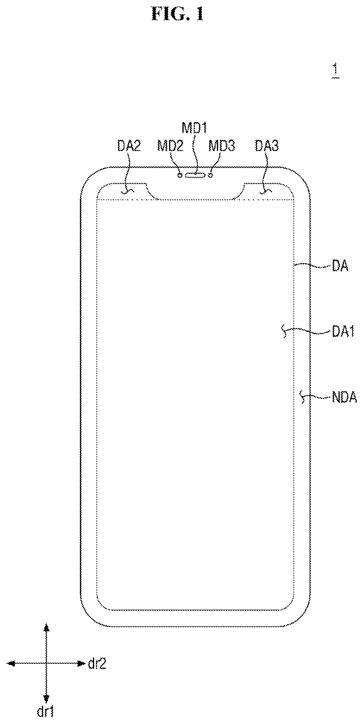
Referring to , an organic light emitting display device 1 has a rectangular shape in which a length in a first direction dr 1 is longer than a length in a second direction dr 2 . For example, the rim of the organic light emitting display device 1 includes long sides extending in the first direction dr 1 and short sides extending in the second direction dr 2 . The rim of the organic light emitting display device 1 includes a curved corner between adjacent long and short sides.
As used herein, for convenience of explanation, the longitudinal direction is defined as a first direction dr 1 , and the direction intersecting the first direction dr 1 is defined as a second direction dr 2 . That is, the second direction dr 2 indicates the horizontal direction in the drawings. However, in embodiments, the present invention is not limited to the aforementioned directions, and it should be understood that the first direction dr 1 and the second direction dr 2 refer to relative directions intersecting each other. Further, for convenience of explanation, based on the center of the drawing, the upper side is defined as one side of the first direction dr 1 , the lower side is defined as the other side of the first direction dr 1 , the left side is defined as one side of the second direction dr 2 , and the right side is defined as the other side of the second direction dr 2 . However, it is obvious that these positions are relative positions.
The organic light emitting display device 1 includes a display area DA and a non-display area NDA.
The display area DA is defined as an area where an image is displayed. The organic light emitting display device 1 may include a plurality of pixels in the display area DA. The display area DA may be used not only as an area for displaying an image but also as an area for recognizing a user's touch input or fingerprint. In an embodiment, the display area DA has one side edge (for example, upper edge in ) having a partially-recessed portion. For example, the one side edge of the display area DA may have a planar bay, notch or trench shape. Here, the display area has a notch shape on the upper edge of the display area DA in which two protrusion portions protrude toward the outside of the display area DA and the recessed portion is relatively indented toward the inside of the display device DA between the two protrusion portions.
In an embodiment, the display area DA includes a first display area DA 1 , a second display area DA 2 protruding from the first display area DA 1 to one side in the first direction dr 1 , and a third display area DA 3 protruding from the first display area DA 1 to one side in the first direction dr 1 . In the drawing, the second display area DA 2 is an area disposed at the left upper left end of the first display area DA 1 , and the third display area DA 3 is an area disposed at the right upper right end of the first display area DA 1 . The second display area DA 2 and the third display area DA 3 are spaced apart from each other along the second direction dr 2 .
The two protrusion portions of the edge of the display area DA include the second display area DA 2 and the third display area DA 3 . Further, the recessed portion may be formed on the upper edge of the first display area DA 1 between the second display area DA 2 and the third display area DA 3 .
The display area DA includes a plurality of rounded corners corresponding to the shape of the rim of the organic light emitting display device 1 . Each rounded corner is disposed between adjacent edges. For example, in the display area DA, rounded corners are disposed at a place where a left edge and an upper edge meet each other, a place where an upper edge and a left edge meet each other, a place where a right edge and a lower edge meet each other, and a place where a lower edge and a left edge meet each other. The rounded corners are disposed adjacent to the corners of the organic light emitting display device 1 .
The non-display area NDA is defined as an area where no image is displayed. The non-display area NDA is disposed outside the display area DA. In an embodiment, the non-display area NDA is a ring-shaped area having an outer rim and an inner rim each having a rectangular shape with rounded corners. The inner rim of the non-display area NDA has a shape including portions protruding toward the recessed portion of the display area DA.
A part of the non-display area NDA is provided with a speaker module MD 1 , a camera module MD 2 , and a sensor module MD 3 . In an embodiment, the speaker module MD 1 , the camera module MD 2 , and the sensor module MD 3 are disposed adjacent to the outer rim of the protrusion portion in the non-display area NDA. As will be described later, various types of wirings bypassing the speaker module MD 1 , the camera module MD 2 , and the sensor module MD 3 may be arranged adjacent to the protrusion portions of the inner rim in the non-display area NDA. In an embodiment, the sensor module MD 3 may include at least one of a luminance sensor, a proximity sensor, an infrared sensor, and an ultrasonic sensor. The arrangement of the speaker module MD 1 , the camera module MD 2 , and the sensor module MD 3 is not limited thereto.
Referring to , in an embodiment, the organic light emitting display device 1 includes a substrate 10 , a circuit layer 20 disposed on the substrate 10 , a light emitting element layer 30 disposed on the circuit layer 20 , an encapsulation layer 40 disposed on the light emitting element layer 30 , a touch layer 50 disposed on the encapsulation layer, and a cover layer 60 disposed on the touch layer 50 . However, the present invention is not limited thereto. Each of the layers may have a single-layer or multi-layer structure, and, if necessary, may be provided with an additional layer or a part thereof may be omitted. A laminate structure of the organic light emitting display device 1 will be described later with reference to , 10 , and 12 .
The touch layer 50 may include a touch sensing unit 50 a that senses a touch input of a user. The arrangement structure of the components constituting the touch layer 50 will be described with reference to .
is a plan view schematically showing a layout structure of a touch sensing unit. is a plan view schematically showing each area of a base layer. is an enlarged plan view showing a layout of the sensing electrode unit of . is an enlarged view of the area FF 1 of . is a cross-sectional view of an organic light emitting display device taken along the line I 1 -I 1 ′ of .
Referring to to 5 , the touch sensing unit 50 a includes sensing electrode units IE 1 and IE 2 , signal wiring units TX, RX, ES, and GL, and a pad terminal unit TPA. The organic light emitting display device 1 includes a base layer BL on which the touch sensing unit 50 a is disposed. One end of each of at least some of the signal wiring units is directly to the sensing electrode units IE 1 and IE 2 , and the other end thereof is directly connected to the pad terminal unit TPA, thereby electrically connecting the sensing electrode units IE 1 and IE 2 to the pad terminal unit TPA. The signal wiring units TX, RX, ES, and GL are disposed in a non-sensing area NAA surrounding the sensing electrode units IE 1 and IE 2 . For convenience of explanation, the space of the non-sensing area NAA where the signal wiring units are disposed is exaggerated in the drawing.
The base layer BL may be a layer on which the sensing electrode units IE 1 and IE 2 , the signal wiring units TX, RX, ES, and GL, and the pad terminal unit TPA are disposed. In an embodiment, the base layer BL may correspond to the encapsulation layer 40 of . However, the present invention is not limited thereto. In another embodiment, the organic light emitting layer may separately include a touch substrate as the base layer BL, and the touch substrate may be directly disposed on the encapsulation layer 40 . The aforementioned touch substrate may be made of glass or plastic such as polyethylene terephthalate (PET), polyimide (PI), polycarbonate (PC), polyethylene (PE), polypropylene (PP), polysulfone (PSF), polymethyl methacrylate (PMMA), triacetyl cellulose (TAC), or a cycloolefin polymer (COP).
The base layer BL may include a plurality of areas. The base layer BL may be provided in substantially the same shape corresponding to the shape of the organic light emitting display device 1 . The base layer BL includes a sensing area AA and a non-sensing area NAA surrounding the outside of the sensing area AA. The sensing area AA may include a plurality of areas, and at least two of the areas may have different areas from each other. For example, the sensing area AA includes first to third sensing areas AA 1 , AA 2 , and AA 3 .
The sensing area AA may have substantially the same shape as the display area DA. The sensing area AA has an edge including a portion indented inward at one side of the sensing area AA. The edge may be the upper edge of the sensing area AA in the drawing. The first to third sensing areas AA 1 , AA 2 and AA 3 may have the same shape corresponding to the first to third display areas DA 1 , DA 2 and DA 3 of the display area DA. That is, the sensing area AA includes a first sensing area AA 1 . The sensing area AA further includes a second sensing area AA 2 and a third sensing area AA 3 , each protruding from the first sensing area AA 1 in the first direction dr 1 . The second sensing area AA 2 and the third sensing area AA 3 are spaced apart from each other, and overlap each other along the second direction dr 2 .
The sensing area AA, like the display area DA, includes a plurality of rounded corners. In an embodiment, the sensing area AA includes a first corner EG 1 disposed at place where a left edge and an upper edge meet each other, a second corner EG 2 disposed at a place where the upper edge and a right edge meet each other, a third corner EG 3 disposed at a place where a lower edge and the left edge meet each other, and a fourth corner EG 4 disposed at a place where the right edge and the lower edge meet each other.
Specifically, the third corner EG 3 and the fourth corner EG 4 are disposed at the left lower side and right lower side of the first sensing area AA 1 , respectively, the first corner EG 1 is disposed at the left upper side of the second sensing area AA 2 , and the second corner EG 2 is disposed at the right upper side of the third sensing area AA 3 . The left upper side and right lower side corners of the second sensing area AA 2 and the right upper side and left lower side corners of the third sensing area AA 3 may be rounded corners. The right lower side corner of the second sensing area AA 2 may be disposed at a place adjacent to the upper edge of the first sensing area AA 1 and at the right edge of the second sensing area AA 2 . The left lower side corner of the third sensing area AA 3 may be disposed at a place adjacent to the upper edge of the first sensing area AA 1 and at the left edge of the third sensing area AA 3 .
When the sensing area AA is formed to have the aforementioned first to fourth corners EG 1 to EG 4 corresponding to the rounded corners of the organic light emitting display device 1 , the dead space of the organic light emitting display device 1 may be reduced. However, the present invention is not limited thereto. Even when the organic light emitting display device 1 has angled rectangular corners, the sensing area AA may be formed to have round corners.
The sensing area AA is defined as an area where the sensing electrode units IE 1 and IE 2 are formed. The sensing electrode units IE 1 and IE 2 are disposed inside the sensing area AA.
The non-sensing area NAA may be defined as an area that is not the sensing area AA. For example, the non-sensing area NAA surrounds the first to third sensing areas AA 1 , AA 2 , and AA 3 with substantially the same shape as the non-display area NDA. The signal wiring units TX, RX, ES, and GL and the pad terminal unit TPA are disposed in the non-sensing area NAA.
The sensing electrode units IE 1 and IE 2 include a plurality of first touch sensing electrodes IE 1 extending in the first direction dr 1 and a plurality of second touch sensing electrodes IE 2 intersecting at least one of the plurality of first touch sensing electrodes IE 1 . The plurality of second sensing electrodes IE 2 extend in the second direction dr 2 .
The sensing electrode units IE 1 and IE 2 may include a sensing electrode and a driving electrode. In this specification, the sensing electrode units IE 1 and IE 2 or the sensing electrode may be used as a term collectively indicating the sensing electrode and the driving electrode.
In the present embodiment, a case where the first touch sensing electrode IE 1 is a driving electrode and the second touch sensing electrode IE 2 is a sensing electrode will be described. Although it is illustrated in the drawing that the plurality of first touch sensing electrodes IE 1 include first to fifth driving electrodes TE 1 to TE 5 and the plurality of second touch sensing electrode IE 2 include first to ninth sensing electrodes RE 1 to RE 9 , the number of the first touch sensing electrodes IE 1 and the number of second touch sensing electrode IE 2 are not limited to that exemplified above.
When the organic light emitting display device 1 has a shape in which a length in the first direction dr 1 is longer than a length in the second direction dr 2 , the length of the first touch sensing electrode IE 1 in the first direction dr 1 is longer than the length of the second touch sensing electrode IE 2 in the second direction dr 2 , but the present invention is not limited thereto.
In an embodiment, the plurality of first touch sensing electrodes IE 1 include a first driving electrode TE 1 extending from the second sensing area AA 2 to the other side of the first direction dr 1 , a fifth driving electrode TE 5 extending from the third sensing area AA 3 to the other side of the first direction dr 1 , and second to fourth driving electrodes TE 2 to TE 4 extending from the first sensing area AA 1 in the first direction dr 1 and disposed between the first driving electrode TE 1 and the fifth driving electrode TE 5 . Each of the first driving electrode TE 1 and the fifth driving electrode TE 5 extends from the second sensing area AA 2 and the third sensing area AA 3 to the first sensing area AA 1 .
The first touch sensing electrodes IE 1 are spaced apart from each other in the second direction dr 2 . For example, the first to fifth driving electrodes TE 1 to TE 5 are sequentially arranged in the second direction dr 2 . The first driving electrode TE 1 and the fifth driving electrode TE 5 are disposed adjacent to both side edges of the sensing area AA in the second direction dr 2 .
The first touch sensing electrode IE 1 may include driving electrode having different extending lengths in the first direction dr 1 . For example, the lengths of the first driving electrode TE 1 and the fifth driving electrode TE 5 , extending from the second sensing area AA 2 and the third sensing area AA 3 to the first sensing area AA 1 , in the first sensing area AA 1 are longer than the lengths of the second to fourth driving electrodes TE 2 to TE 4 , extending only from the first sensing area AA 1 , in the first direction dr 1 .
Each driving electrode may include at least one driving electrode pattern. For example, the first driving electrode TE 1 and the fifth driving electrode TE 5 include first to ninth driving electrode patterns TE 11 to TE 19 and TE 51 to TE 59 sequentially spaced apart from each other along the first direction dr 1 . The second, third and fourth driving electrodes TE 2 , TE 3 and TE 4 include first to eighth driving electrode patterns TE 21 to TE 28 , TE 31 to TE 38 , and TE 41 to TE 48 sequentially spaced apart from each other along the first direction dr 1 .
The first driving electrode pattern TE 11 of the first driving electrode TE 1 and the first driving electrode pattern TE 51 of the fifth driving electrode TE 5 may be disposed in the second sensing area AA 2 and the third sensing area AA 3 without overlapping the second to fourth driving electrodes TE 2 to TE 4 in the second direction dr 2 . The second to ninth driving electrode patterns TE 12 to TE 19 and TE 52 to TE 59 may overlap the first to eighth driving electrode patterns TE 21 to TE 28 , TE 31 to TE 33 , and TE 41 to TE 46 of the second to fourth driving electrode TE 2 to TE 4 in the second direction dr 2 . In an embodiment, the second driving electrode pattern TE 12 of the first driving electrode TE 1 is disposed in the sensing area AA 2 and the first sensing area AA 1 and at the boundary between the sensing area AA 2 and the first sensing area AA 1 . In an embodiment, the second driving electrode pattern TE 52 of the fifth driving electrode TE 5 is disposed in the third sensing area AA 3 and the first sensing area AA 1 and at the boundary between the third sensing area AA 3 and the first sensing area AA 1 . The first driving electrode TE 1 and the fifth driving electrode TE 5 include an area overlapping the second to fourth driving electrodes TE 2 to TE 4 in the second direction dr 2 and an area non-overlapping the second driving electrode TE 2 to TE 4 in the second direction dr 2 . Further, the first driving electrode TE 1 and the fifth driving electrode TE 5 overlap each other in the second direction dr 2 in the area non-overlapping the second to fourth driving electrodes TE 2 to TE 4 .
The plurality of second touch sensing electrodes IE 2 include a first sub-touch sensing electrode unit IE 2 a continuously extending from one side edge of the first sensing area AA 1 to the other side edge thereof in the second direction dr 2 and a second sub-touch sensing electrode unit IE 2 b disposed in the second sensing area AA 2 and the third sensing area AA 3 and extending in the second dr 2 . The first sub-touch sensing electrode unit IE 2 a and the second sub-touch sensing electrode unit IE 2 b may include at least one sensing electrode. For example, the first sub-touch sensing electrode unit IE 2 a includes first to seventh sensing electrodes RE 1 to RE 7 , and the second sub-touch sensing electrode unit IE 2 b includes eighth and ninth sensing electrodes RE 8 and RE 9 .
The first to seventh sensing electrodes RE 1 to RE 7 of the first sub-touch sensing electrode unit IE 2 a are spaced apart from each other in the first direction dr 1 . For example, the first to seventh sensing electrodes RE 1 to RE 7 are sequentially arranged in the first direction dr 1 .
The second sub-touch sensing electrode unit IE 2 b is adjacent to and spaced apart from the first sub-touch sensing electrode unit IE 2 a in the first direction dr 1 . In an embodiment, the eighth sensing electrode RE 8 and the ninth sensing electrode RE 9 are disposed adjacent to and spaced apart from the first sensing electrode RE 1 in the first direction dr 1 .
In an embodiment, the plurality of first to seventh sensing electrodes RE 1 to RE 7 have the same extending length in the second direction dr 2 . Meanwhile, the lengths of the first sub-touch sensing electrode unit IE 2 a and the second sub-touch sensing electrode unit IE 2 b in the second direction dr 2 are different from each other. For example, the length of the first sub-touch sensing electrode unit IE 2 a in the second direction dr 2 is longer than the length of the second sub-touch sensing electrode unit IE 2 b in the second direction dr 2 .
The second sub-touch sensing electrode unit IE 2 b may have the same shape as a part of the middle portion of the first sensing electrode RE 1 cut off. For example, the second sub-touch sensing electrode unit IE 2 b has a shape having only a portion including one end of the first sensing electrode RE 1 and a portion including the other end thereof.
The second sub-touch sensing electrode unit IE 2 b includes an eighth sensing electrode RE 8 disposed in the second sensing area AA 2 and a ninth sensing electrode RE 9 disposed in the third sensing area AA 3 . The eighth sensing electrode RE 5 and the ninth sensing electrode RE 9 are disposed on the same virtual straight line extending in the second direction dr 2 . For example, the eighth sensing electrode RE 8 and the ninth sensing electrode RE 9 are spaced apart from each other in the second direction dr 2 and overlap each other in the second direction dr 2 .
Each of the sensing electrodes RE to RE 9 may include at least one sensing electrode pattern. For example, the first to seventh sensing electrodes RE 1 to RE 7 include first to sixth sensing electrode patterns RE 11 to RE 16 , RE 21 to RE 26 , RE 31 to RE 36 , RE 41 to RE 46 , RE 51 to RE 56 , RE 61 to RE 66 , and RE 71 to RE 76 , which are sequentially arranged to be spaced apart from each other. The eighth sensing electrode RE 8 and the ninth sensing electrode RE 9 include first sensing electrode patterns RE 81 and RE 91 and second sensing electrode patterns RE 82 and RE 92 , which are arranged in the second direction dr 2 . The areas of the first sensing electrode pattern RE 81 and the second sensing electrode pattern RE 82 of the eighth sensing electrode RE 8 may be different from each other. For example, the area of the first sensing electrode pattern RE 81 of the eighth sensing electrode RE 8 is larger than the area of the second sensing electrode pattern RE 82 thereof. Similarly, the areas of the first sensing electrode pattern RE 91 and the second sensing electrode pattern RE 92 of the ninth sensing electrode RE 9 may be different from each other. For example, the area of the second sensing electrode pattern RE 92 of the ninth sensing electrode RE 9 is larger than the area of the first sensing electrode pattern RE 91 thereof.
Meanwhile, the sensing electrode patterns adjacent to each other in each of the sensing electrodes RE 1 to RE 9 in the second direction dr 2 may be physically connected to each other. For example, a connection portion CP connecting the sensing electrode patterns adjacent to each other in the second direction dr 2 is disposed between the driving electrode patterns adjacent to each other in the first direction dr 1 of the first touch sensing electrode IE 1 . For example, the first sensing electrode pattern RE 11 and second sensing electrode pattern RE 12 of the first sensing electrode RE 1 are physically connected to each other through the connection portion CP, whereas the second driving electrode pattern TE 12 and third driving electrode pattern TE 13 of the first driving electrode TE 1 are physically separated from each other by the connection portion CP.
The first sensing electrode pattern RE 81 and second sensing electrode pattern RE 82 of the eighth sensing electrode RE 8 may be physically connected to each other using the connection portion CP disposed between the first driving electrode pattern TE 11 and second driving electrode pattern TE 12 of the first driving electrode TE 1 . The first driving electrode pattern TE 11 and the second driving electrode pattern TE 12 may be physically separated from each other by the connection portion CP. Similarly, the first sensing electrode pattern RE 91 and second sensing electrode pattern RE 92 of the ninth sensing electrode RE 9 may be physically connected to each other using the connection portion CP disposed between the first driving electrode pattern TE 51 and second driving electrode pattern TE 52 of the fifth driving electrode TE 5 . The first driving electrode pattern TE 51 and the second driving electrode pattern TE 52 may be physically separated from each other by the connection portion CP. In this case, the second sensing electrode pattern RE 82 of the eight sensing pattern RE 8 and the first sensing electrode pattern RE 91 of the ninth sensing electrode RE 9 are disposed between the first driving electrode TE 1 and the fifth driving electrode TE 5 .
The eighth sensing electrode RE 8 traverses only the first driving electrode TE 1 without traversing the second to fifth driving electrodes TE 2 to TE 5 . The ninth sensing electrode RE 9 traverses only the fifth driving electrode TE 5 without traversing the first to fourth driving electrodes TE 1 to TE 4 . The first to seventh sensing electrodes RE to RE 7 traverse all the driving electrodes TE 1 to TE 5 .
In an embodiment, each of the sensing electrode patterns disposed at one end and the other end of the first touch sensing electrode IE 1 and the second touch sensing electrode IE 2 may have an approximately rhombus shape. Each of the sensing electrode patterns disposed at one end and the other end of the first touch sensing electrode IE 1 and the second touch sensing electrode IE 2 may have an isosceles triangle shape in which the rhombus shape is cut in half. Each of the driving electrode patterns TE 11 to TE 59 and each of the sensing electrode patterns RE 11 to RE 92 may include at least one zigzag-shaped side. For example, each of the sides of the rhombic driving electrode pattern (for example, TE 12 ) and the rhombic sensing electrode pattern (for example, RE 12 ) may have a zigzag shape. Further, two isosceles of an isosceles triangular driving electrode pattern (for example, TE 11 ) and an isosceles triangular sensing electrode pattern (for example, RE 11 ) may have a zigzag shape, and the other one may have a linear shape. When each of the driving electrode patterns TE 11 to TE 59 and each of the sensing electrode patterns RE 11 to RE 92 include zigzag-shaped sides, it is possible to prevent a moire pattern from being viewed to a user, and it is possible to prevent the display failure of the organic light emitting display device 1 due to a moire pattern.
Since the sensing area AA includes rounded corners EG 1 to EG 4 , each of the sensing electrode units IE 1 and IE 2 adjacent to the rounded corners EG 1 to EG 4 of the sensing area AA may have shapes cut according to the shapes of the rounded corners EG 1 to EG 4 of the sensing area AA. For example, the first driving electrode pattern TE 11 and ninth driving electrode pattern TE 19 of the first driving electrode TE 1 , the first driving electrode pattern TE 15 and ninth driving electrode pattern TE 59 of the fifth driving electrode TE 5 , the first sensing electrode pattern RE 71 and sixth sensing electrode pattern RE 76 of the seventh sensing electrode RE 7 , the first sensing electrode pattern RE 81 and second sensing electrode pattern RE 82 of the eighth sensing electrode RE 8 have shapes cut according to the shapes of the rounded corners EG 1 to EG 4 of the sensing area AA. The position and area where the sensing electrode units IE 11 and IE 12 are cut off may be determined by the radius of curvature of the rounded corners EG 1 to EG 4 of the sensing area AA.
Additionally, referring to , the sensing area AA further includes island electrodes IS 1 and IS 2 disposed inside the second touch sensing electrode IE 2 and insulated and spaced from the second touch sensing electrode IE 2 . The driving electrode patterns adjacent to each other of the first touch sensing electrode IE 1 may be electrically connected to each other through the island electrodes IS 1 and IS 2 . For convenience of explanation, in the drawing, a portion where the first sensing electrode RE 1 intersects the first driving electrode TE 1 will be described as an example, but it will be understood that the same configuration is disposed at a place where each of the driving electrodes TE 1 to TE 5 intersects each of the sensing electrodes RE 1 to RE 7 .
In an embodiment, the first island electrode IS 1 and the second island electrode IS 2 disposed between the first sensing electrode pattern RE 11 and second sensing electrode pattern RE 12 of the first sensing electrode RE 1 are disposed in the sensing area AA. The first island electrode IS 1 is disposed between the first sensing electrode pattern RE 11 and the connection CP in the first sensing electrode RE 1 . The second island electrode IS 2 is disposed between the second sensing electrode pattern RE 12 and the connection CP in the first sensing electrode RE 1 .
The second driving electrode pattern TE 12 and first island electrode IS 1 of the first driving electrode TE 1 may be electrically connected to each other through a first bridge wiring BE 1 , and the third driving electrode pattern TE 13 and first island electrode IS 1 of the first driving electrode TE 1 may be electrically connected to each other through a second bridge wiring BE 2 . Further, the second driving electrode pattern TE 12 and second island electrode IS 2 of the first driving electrode TE 1 may be electrically connected to each other through a third bridge wiring BE 3 , and the third driving electrode pattern TE 13 and second island electrode IS 2 of the first driving electrode TE 1 may be electrically connected to each other through a fourth bridge wiring BE 4 . The second driving electrode pattern TE 12 and third driving electrode pattern TE 13 of the first driving electrode TE 1 may be electrically connected to each other through the first island electrode IS 1 , the second island electrode IS 2 , and the first to fourth bridge wirings BE 1 to BE 4 .
As described above, the two island electrodes IS 1 and IS 2 are disposed between the second driving electrode pattern TE 12 and third driving electrode pattern TE 13 of the first driving electrode TE 1 in the first direction dr 1 . Even when any one of the first to fourth bridge wirings BE 1 to BE 4 is disconnected, the second driving electrode pattern TE 12 and third driving electrode pattern TE 13 of the first driving electrode TE 1 may still be electrically connected to each other
The island electrodes IS 1 and IS 2 , as shown in the drawings, have a diamond shape, but the shape thereof is not limited thereto. The island electrodes IS 1 and IS 2 may have various shapes such as a square or another polygon, a circle, and an ellipse.
When the driving electrode patterns of the first sensing electrode IE 1 are connected through the island electrodes IS 1 and IS 2 , the margin of the bridge wirings may be reduced, compared to when the driving electrode patterns of the first sensing electrode IE 1 are connected through one bridge wiring without going through the island electrodes. That is, the lengths of the bridge wirings BE 1 to BE 4 may be reduced. As a result, transmittance may be improved by reducing overlap between the bridge wirings BE 1 to BE 4 and the display area DA. Further, since the contact area between the first sensing electrode IE 1 and the bridge wirings BE 1 to BE 4 is increased, the contact resistance therebetween may be improved.
The lamination relationship of the island electrodes IS 1 and IS 2 , the bridge wirings BE 1 to BE 4 , the driving electrode patterns, the sensing electrode patterns, and other components of the organic light emitting display device will be described later.
Next, a relationship between the unit sensing area and the sensing electrode unit will be described with reference to .
is a plan view of the sensing electrode unit of divided into unit sensing areas.
Referring to , the driving electrode patterns TE 11 to TE 59 of the driving electrodes TE 1 to TE 5 and the sensing electrode patterns of the sensing electrodes RE 1 to RE 9 , adjacent to each other, may constitute unit sensing areas. For example, based on an area where the driving electrodes TE 1 to TE 5 and the sensing electrodes RE 1 to RE 9 intersect each other, one of the two driving electrode patterns (for example, TE 22 and TE 32 ) adjacent to each other in the second direction dr 2 and one of the two sensing electrode patterns (for example, RE 13 and RE 23 ) adjacent to each other in the first direction dr 1 may constitute one square or rectangle. As such, the area defined by the half of the adjacent driving electrode patterns and sensing electrode patterns may be one unit sensing area SUT. In the unit sensing area SUT, the capacitance values between the adjacent driving electrode patterns and sensing electrode patterns are measured, thereby determining whether or not a touch input is applied and calculating the corresponding position as touch input coordinates. The touch sensing may be performed by a mutual capping method, but is not limited thereto.
Each unit sensing area SUT may be larger than a pixel in size. For example, the unit sensing area SUT may correspond to a plurality of pixels. The length of one side of the unit sensing area SUT may be in a range of 4 mm to 5 mm, but is not limited thereto.
Meanwhile, the plurality of unit sensing areas SUT are arranged in row and column directions. Here, the row and column directions may refer to the second direction dr 2 and the first direction dr 1 , respectively. For example, as shown in the drawing, the plurality of unit sensing areas SUT may be in the form of a matrix of eight rows and five columns. However, some of the plurality of unit sensing areas SUT may include areas where the sensing electrode units IE 1 and IE 2 are not provided. For example, the areas of first row and second column, first row and third column and first row and fourth column may be areas where the sensing electrode units IE 1 and IE 2 are not disposed substantially due to the atypical edge of the sensing area AA. Therefore, the arrangement form of the plurality of unit sensing areas SUT may be one in which first row and second column, first row and third column and first row and fourth column of the matrix of eight rows and five columns are omitted.
The ratio of the area occupied by the sensing electrode units IE 1 and IE 2 in each unit sensing area SUT may not be the same. In particular, since the sensing area AA includes atypical edges and rounded corners, the ratio of the area occupied by the sensing electrode units IE 1 and IE 2 in the unit sensing area SUT including atypical edges and the unit sensing area SUT including rounded corners may be small as compared with in the unit sensing area SUT not including atypical edges and rounded corners.
If the ratio (hereinafter, referred to as an area ratio) of the area occupied by the sensing electrode units IE 1 and IE 2 in the unit sensing area SUT is defined as 1 in the unit sensing area SUT where the sensing electrode units IE 1 and IE 2 are not cut off (for example, the unit sensing area SUT of second row and second column), in an embodiment, the area ratio of the unit sensing area SUT where the sensing electrode units IE 1 and IE 2 are not cut off (for example, the unit sensing area SUT of first row and first column, including the corner EG 1 ) may be 0.6 to 0.8, but is not limited thereto. In another embodiment, the area ratio of the unit sensing area SUT where the sensing electrode units IE 1 and IE 2 are not cut off may have various values of less than 1.
As the ratio of the area occupied by the sensing electrode units IE 1 and IE 2 in each unit sensing area SUT increases, touch sensitivity and touch performance may be improved. For example, the touch sensitivity in the unit sensing area SUT having an area ratio of 1 may be higher than the touch sensitivity in the unit sensing area SUT having an area ratio of 0.6.
For convenience of explanation, the unit sensing area SUT having an area ratio of 1 will be referred to as a first unit sensing area SUT 1 , and the unit sensing area SUT having an area ratio of less than 1 will be referred to as a second unit sensing area SUT 2 . For example, the second unit sensing area SUT 2 may include unit sensing areas (unit sensing areas of first row and first column, first row and fifth column, eighth row and first column, and eighth row and fifth column). The first unit sensing area SUT 1 may include, for example, a unit sensing unit SUT of third row and second column).
The second unit sensing area SUT 2 may require a compensation design to increase the touch sensitivity by the first unit sensing area SUT. First, a connection relationship between the signal wiring units TX, RX, ES, and GL and the sensing electrode units IE 1 and IE 2 will be described.
is an enlarged view of the area FF 2 of . is a cross-sectional view of a part of an organic light emitting display device taken along the line I 2 -I 2 ′ of .
Referring to together with , driving signals may be transmitted to the driving electrodes TE 1 to TE 5 through the touch driving wirings TX 1 _ 1 to TX 5 _ 1 and TX 1 _ 2 to TX 5 _ 2 , and sensing signals may be transmitted to the sensing electrodes RE 1 to RE 9 through the touch sensing wirings RX 1 _ 1 to RX 8 _ 1 .
The touch driving wirings TX 1 _ 1 to TX 5 _ 1 and TX 1 _ 2 to TX 5 _ 2 are connected to each of the driving electrodes TE 1 to TE 5 . In an embodiment, the plurality of touch driving wirings TX 1 _ 1 to TX 5 _ 1 and TX 1 _ 2 to TX 5 _ 2 may be connected to each of the driving electrode TE 1 to TE 5 . That is, each of the driving electrodes TE 1 to TE 5 may be double-routed. For example, the touch driving wirings TX 1 _ 1 to TX 5 _ 1 and TX 1 _ 2 to TX 5 _ 2 include first touch driving wirings TX 1 _ 1 to TX 5 _ 1 connected to the lower end of each of the driving electrodes TE 1 to TE 5 and second touch driving wirings TX 1 _ 2 to TX 5 _ 2 connected to the upper end of each of the driving electrodes TE 1 to TE 5 .
In an exemplary embodiment, the second touch driving wrings TX 1 _ 2 to TX 5 _ 2 may be mainly disposed on one side of the non-sensing area NAA in the second direction, and the touch sensing wrings RX 1 _ 1 to RX 8 _ 1 may be mainly disposed on one side of the non-sensing area NAA in the second direction.
The first touch driving wirings TX 1 _ 1 to TX 5 _ 1 extend from the pad terminal unit TPA to one side and/or the other side in the second direction dr 2 and are connected to the lower ends of the driving electrodes TE 1 to TE 5 .
The second touch driving wirings TX 1 _ 2 to TX 5 _ 2 extend from the pad terminal unit TPA to one side in the second direction dr 2 , bypass the left edge of the display area DA, and bypass the upper edge of the display area DA including protrusion portions to be connected to the upper end of each of the driving electrodes TE 1 to TE 5 .
In an embodiment, when at least some of the second touch driving wirings TX 1 _ 2 to TX 5 _ 2 bypass the upper edge of the sensing area AA, they bypass an area where the speaker module MD 1 , the camera module MD 2 , and the sensor module MD 3 are disposed in the second sensing area AA 2 , the third sensing area AA 3 , and the non-display area NDA. For example, when the second touch driving wirings TX 1 _ 2 to TX 5 _ 2 connected to the first to fifth driving electrodes TE 1 to TE 5 bypass the upper edge of the sensing area AA, they extend approximately in the second direction dr 2 with portions extending in the first direction dr 1 to bypass an area where the speaker module MD 1 , the camera module MD 2 , and the sensor module MD 3 are disposed.
The second to fourth wirings TX 2 _ 2 to TX 4 _ 2 of the second touch driving wirings TX 1 _ 2 to TX 5 _ 2 connected to the second to fourth driving electrodes TE 2 to TE 4 include a portion disposed between the eighth sensing electrode RE 8 and the ninth sensing electrode RE 9 . The second to fourth wirings TX 2 _ 2 to TX 4 _ 2 of the second touch driving wirings TX 1 _ 2 to TX 5 _ 2 connected to the second to fourth driving electrodes TE 2 to TE 4 include a portion overlapping the eighth sensing electrode RE 8 and the ninth sensing electrode RE 9 in the second direction dr 2 .
The touch sensing wirings RX 1 _ 1 to RX 8 _ 1 are connected to the respective sensing electrodes RE 1 to RE 9 . In an embodiment, unlike the driving electrodes TE 1 to TE 5 , each of the first to seventh sensing electrodes RE 1 to RE 7 and the ninth sensing electrode RE 9 is connected to the touch sensing wiring RX 1 _ 1 to RX 8 _ 1 at only one end thereof, but the present invention is not limited thereto.
In an embodiment, each of the touch sensing wirings RX 1 _ 1 to RX 8 _ 1 connected to the first to seventh sensing electrodes RE 1 to RE 7 and the ninth sensing electrode RE 9 extends from the pad terminal unit TPA to the lower side of the non-sensing area NAA in the first direction dr 1 and then turns to the other side thereof in the second direction dr 2 , and further extends from the outside of the right edge of the sensing area AA in the first direction dr 1 to the right ends (for example, RE 16 , RE 26 , RE 36 , RE 46 , RE 56 , RE 76 , and RE 92 ) of the first to seventh sensing electrodes RE 1 to RE 7 and the ninth sensing electrode RE 9 for connections between the touch sensing wirings RX 1 _ 1 to RX 8 _ 1 to the sensing electrodes RE 1 to RE 7 and RE 9 . For example, in the first to seventh sensing electrodes RE 1 to RE 7 , the touch sensing wirings RX 2 _ 1 to RX 8 _ 1 are connected only to the ends of the respective sixth sensing electrode patterns RE 16 , RE 26 , RE 36 , RE 46 , RE 56 and RE 76 . Further, in the ninth sensing electrode RE 9 , the touch sensing wiring RX 1 _ 1 is connected only to the end of the second sensing electrode pattern RE 92 of the ninth sensing electrode RE 9 .
Meanwhile, a connection wiring RX 1 _ 2 for connecting the eighth sensing electrode RE 8 and the ninth sensing electrode RE 9 is provided between the eighth sensing electrode RE 8 and the ninth sensing electrode RE 9 . Thus, the connection wiring RX 1 _ 2 traverses some of the second touch driving wirings TX 1 _ 2 to TX 5 _ 2 . For example, the connection wiring RX 1 _ 2 traverses the second to fourth wirings TX 2 _ 2 to TX 4 _ 2 of the second touch driving wirings TX 1 _ 2 to TX 5 _ 2 . In this case, to prevent a short circuit between the second to fourth wirings TX 2 _ 2 to TX 4 _ 2 of the second touch driving wirings TX 1 _ 2 to TX 5 _ 2 and the connection wiring RX 1 _ 2 , the second to fourth driving electrodes TE 2 to TE 4 and the second to fourth wirings TX 2 _ 2 to TX 4 _ 2 of the second touch driving wirings TX 1 _ 2 to TX 5 _ 2 are connected to each other through a driving bridge electrode portion (for example, TE 31 a ) extending from the second to fourth driving electrodes TE 2 to TE 4 .
The connection wiring RX 1 _ 2 traverses the driving bridge electrode portion TE 31 a and extends in the second direction dr 2 from the eighth sensing electrode RE 8 to the ninth sensing electrode RE 9 . An insulating material (for example, a first touch insulating layer 511 in ) is disposed between the driving bridge electrode portion TE 31 a and the connection wiring RX 1 _ 2 .
In an embodiment, the eighth sensing electrode RE 8 need not be directly connected to the touch sensing wirings RX 1 _ 1 to RX 8 _ 1 connected to the pad terminal unit TPA. The eighth sensing electrode RE 8 and the ninth sensing electrode RE 9 are electrically connected to each other through the connection wiring RX 1 _ 2 , and the touch sensing wiring RX 8 _ 1 connected to the ninth sensing electrode RE 9 is connected to the pad terminal unit TPA, so that the eighth sensing electrode RE 8 and the ninth sensing electrode RE 9 may receive the same sensing signal.
Meanwhile, the driving voltage signal provided to each of the driving electrodes TE 1 to TE 5 may be a driving voltage signal having a voltage level higher than a sensing voltage signal provided to each of the sensing electrodes RE 1 to RE 9 . When a signal of a relatively high voltage level is provided to each of the driving electrodes TE 1 to TE 5 , the voltage level in the touch sensing electrode may vary greatly for each position depending on the distance between the driving electrode and the wiring. For example, when one of the touch driving wirings TX 1 _ 1 to TX 5 _ 1 is connected only to one end of each of the driving electrodes TE 1 to TE 5 , the voltage level at the first driving electrode pattern (for example, TE 11 or TE 21 ) and the voltage level at the eighth or ninth driving electrode pattern (for example, TE 19 or TE 28 ) may be greatly different from each other. The plurality of touch driving wirings TX 1 _ 1 to TX 5 _ 1 and TX 1 _ 2 to TX 5 _ 2 are connected to each of the driving electrodes TE 1 to TE 5 , so that the difference between the voltage levels of the driving electrode patterns of the respective driving electrodes TE 1 to TE 5 may be minimized.
Antistatic wirings ES 1 and ES 2 are disposed at the outermost portions of the touch driving wirings TX 1 _ 1 to TX 5 _ 1 and TX 1 _ 2 to TX 5 _ 2 and the touch sensing wirings RX 1 _ 1 to RX 8 _ 1 arranged to surround the sensing electrode units IE 1 and IE 2 . In an embodiment, the antistatic wirings ES 1 and ES 2 include a first antistatic wiring ES 1 and a second antistatic wiring ES 2 . The first and second antistatic wirings ES 1 and ES 2 surround the display area DA, the touch driving wirings TX 1 _ 1 to TX 5 _ 1 and TX 1 _ 2 to TX 5 _ 2 and the touch sensing wirings RX 1 _ 1 to RX 8 _ 1 in a ring shape. The first antistatic wiring ES 1 and the second antistatic wiring ES 2 need not be connected to each other.
The first antistatic wiring ES 1 surrounds the touch sensing wirings RX 1 _ 1 to RX 8 _ 1 located on the right and lower sides of the display area DA.
The second antistatic wiring ES 2 may cover the touch driving wirings TX 1 _ 1 to TX 5 _ 1 and TX 1 _ 2 to TX 5 _ 2 located on the left, upper and lower sides of the display area DA.
Each of the antistatic wirings ES 1 and ES 2 may be a wiring to which a first reference voltage applies. Each of the antistatic wirings ES 1 and ES 2 may serve to alleviate an electrostatic shock that may apply to the touch driving wirings TX 1 _ 1 to TX 5 _ 1 and TX 1 _ 2 to TX 5 _ 2 , the touch sensing wirings RX 1 _ 1 to RX 8 _ 1 and the sensing electrode units IE 1 and IE 2 .
Guard wirings GL 1 to GL 4 are disposed between the touch driving wirings TX 1 _ 1 to TX 5 _ 1 and TX 1 _ 2 to TX 5 _ 2 and the touch sensing wirings RX 1 _ 1 to RX 8 _ 1 and/or between the touch driving wirings TX 1 _ 1 to TX 5 _ 1 and TX 1 _ 2 to TX 5 _ 2 and the touch sensing wirings RX 1 _ 1 to RX 8 _ 1 and the respective antistatic wirings ES 1 and ES 2 . The guard wirings GL 1 to GL 4 include a first guard wiring GL 1 , a second guard wiring GL 2 , a third guard wiring GL 3 , and a fourth guard wiring GL 4 .
The first guard wiring GL 1 is disposed between the touch sensing wiring lines RX 1 _ 1 to RX 8 _ 1 extending to the right side of the non-sensing area NAA and the first antistatic wiring ES 1 .
The second guard wiring GL 2 is disposed between the first touch driving wirings TX 1 _ 1 to TX 5 _ 1 connected to the lower end of the first touch sensing electrode IE 1 and the touch sensing wirings RX 1 _ 1 to RX 8 _ 1 extending to the right side of the non-sensing area NAA.
The third guard wiring GL 3 is disposed between the first touch driving wirings TX 1 _ 1 to TX 5 _ 1 and the second touch driving wirings TX 1 _ 2 to TX 5 _ 2 on the lower side of the non-sensing area NAA, and is disposed between the second touch driving wirings TX 1 _ 2 to TX 5 _ 2 and the sensing electrode units IE 1 and IE 2 on the left side of the non-sensing area NAA. For example, the third guard wiring GL 3 is disposed between a first wiring portion (TX 1 _ 2 a in ) of the first wiring TX 1 _ 2 of the second touch driving wirings TX 1 _ 2 to TX 5 _ 2 and the sensing electrode units IE 1 and IE 2 on the left side of the non-sensing area NAA. The first wiring portion TX 1 _ 2 a will be described with reference to .
The fourth guard wiring GL 4 is disposed between the second touch driving wirings TX 1 _ 2 to TX 5 _ 2 connected to the upper end of the first touch sensing electrode IE 1 and the second antistatic wiring ES 2 .
Each of the guard wirings GL 1 to GL 4 is a wiring through which a second reference voltage signal flows. Each of the guard wirings GL 1 to GL 4 may prevent a signal interference phenomenon that may occur between adjacent wirings.
In an embodiment, the pad terminal unit TPA is disposed on the right side of the lower end of the non-sensing area NAA. The position of the pad terminal unit TPA is not limited thereto, and may vary depending on the electrical connection relationship with the elements other than the touch sensing unit 50 a . The pad terminal unit TPA may include pad terminals connected to the touch driving wirings TX 1 _ 1 to TX 5 _ 1 and TX 1 _ 2 to TX 5 _ 2 , touch sensing wirings RX 1 _ 1 to RX 8 _ 1 , guard wirings GL 1 to GL 4 and antistatic wirings ES 1 and ES 2 .
Next, a compensation design of the second unit sensing area will be described. For convenience of explanation, a unit sensing area SUT of one row and one column including the first corner EG 1 , of the second unit sensing area SUT 2 , will be described as an example.
is an enlarged view of the area FF 3 of . is a cross-sectional view of an organic light emitting display device taken along the line I 3 -I 3 ′ of .
The first driving electrode pattern TE 11 of the first driving electrode TE 1 is connected to the first wiring TX 1 _ 2 of the second touch driving wirings TX 1 _ 2 to TX 5 _ 2 . The first wiring TX 1 _ 2 of the second touch driving wirings TX 1 _ 2 to TX 5 _ 2 includes a first wiring portion TX 1 _ 2 a having a first line width L 1 and a first junction portion TX 1 _ 2 b having a second line width L 2 larger than the first line width L 1 . The first junction portion TX 1 _ 2 b is connected to the first driving electrode pattern TE 11 of the first driving electrode TE 1 .
Like the first wiring TX 1 _ 2 , each of the second to fifth wirings TX 2 _ 2 to TX 5 _ 2 of the second touch driving wirings TX 1 _ 2 to TX 5 _ 2 may include a wiring portion and a junction portion.
The second line width L 2 is larger than the sum of the first line width L 1 and the line width of the third guard wiring GL 3 adjacent to the first wiring TX 1 _ 2 of the second touch driving wirings TX 1 _ 2 to TX 5 _ 2 .
In an embodiment, the first line width L 1 of the first junction portion TX 1 _ 2 b may occupy 30% or more of the width L 3 of an area where the second touch driving wirings TX 1 _ 2 to TX 5 _ 2 , the fourth guard wiring GL 4 and the second antistatic wiring ES 2 are disposed at the upper side of the non-sensing area NAA. The total width L 3 of the non-sensing area NAA in which the wirings are arranged may be about 250 μm to about 350 μm. The total width L 3 may refer to a width occupied by the second touch driving wirings TX 1 _ 2 to TX 5 _ 2 , the fourth guard wiring GL 4 , and the second antistatic wiring ES 2 , and may be a width including intervals between the respective wirings.
The first line width L 1 of the first wiring portion TX 1 _ 2 a may be about 15 μm to about 25 μm. The first wiring portion TX 1 _ 2 a extends from one side of the first junction portion TX 1 _ 2 b . A portion of the first wiring portion TX 1 _ 2 a extending along the outside of the first corner EG 1 may have a curved shape, a portion of the first wiring portion TX 1 _ 2 a extending along the left edge of the non-sensing area may have a linear shape, and a portion of the first wiring portion TX 1 _ 2 a extending along the outside of the third corner EG 3 may have a curved shape.
The second line width L 2 of the first junction portion TX 1 _ 2 b may be about 90 μm to about 110 μm. The second line width L 2 may be a width occupied by the first junction portion TX 1 _ 2 b in the normal line direction of the extending direction of the first corner EG 1 . The first junction portion TX 1 _ 2 b may include a portion overlapping the first driving electrode pattern TE 11 of the first driving electrode TE 1 in the thickness direction. The first driving electrode pattern TE 11 of the first driving electrode TE 1 may be in contact with the overlapped portion of the first junction portion TX 1 _ 2 b through a first contact hole CNT 1 of a first touch insulating layer 511 disposed between the first junction portion TX 1 _ 2 b and the first driving electrode pattern TE 11 .
In an embodiment, the first contact hole CNT 1 may have a shape extending in a direction similar to the first corner EG 1 . For example, the first contact hole CNT 1 has a shape extending in the normal line of the second line width L 2 . That is, the first contact hole CNT 1 may extend in a direction parallel to the first corner EG 1 .
In an embodiment, the width L 4 of a portion where the first driving electrode pattern TE 11 of the first driving electrode TE 1 overlaps the first junction portion TX 1 _ 2 b in the thickness direction may be about 15 μm to about 25 μm, but is not limited thereto.
Referring to , the first driving electrode pattern TE 31 of the third driving electrode TE 3 may be connected to the third wiring TX 3 _ 2 of the second touch driving wirings TX 1 _ 2 to TX 5 _ 2 .
The third wiring TX 3 _ 2 of the second touch driving wirings TX 1 _ 2 to TX 5 _ 2 includes a second wiring portion TX 3 _ 2 a having a third line width L 5 and a second junction portion TX 3 _ 2 b having a fourth line width L 6 larger than the third line width L 5 . The second junction portion TX 3 _ 2 b may be connected to a driving bridge electrode portion TE 31 a of the third driving electrode TE 3 .
When the first driving electrode pattern TE 31 of the third driving electrode TE 3 is cut off by the sensing area AA, the area ratio in the unit sensing area (SUT) is less than 1, so that a compensation design may be required. For this purpose, the fourth line width L 6 may be adjusted.
The fourth line width L 6 is larger than the width L 7 of a portion where the driving bridge electrode portion TE 31 a and the second junction portion TX 3 _ 2 b overlap each other. Further, in an embodiment, the fourth wiring width L 6 may be equal to or less than the second wiring width L 2 .
Hereinafter, a connection relationship of a laminate structure of the touch sensing unit 50 a and other members of the organic light emitting display device 1 will be described with reference to , 7 , 10 , and 12 .
The touch layer 50 including the touch sensing unit 50 a includes a first touch conductive layer, a first touch insulating layer 511 , a second touch conductive layer, and a second touch insulating layer 512 , which are sequentially disposed on the encapsulation layer 40 .
The first touch conductive layer is disposed on the encapsulation layer 40 . For example, the first touch conductive layer may be disposed on a second inorganic film 453 to be described later. The first touch conductive layer may include at least one selected from molybdenum (Mo), aluminum (Al), platinum (Pt), palladium (Pd), silver (Ag), magnesium (Mg), gold (Au), nickel (Ni), neodymium (Nd), iridium (Ir), chromium (Cr), calcium (Ca), titanium (Ti), tantalum (Ta), tungsten (W), and copper (Cu). The first touch conductive layer may be a single-layer film or a multi-layer film.
As described above, the first touch conductive layer may include the bridge wirings BE 1 and BE 2 , the touch driving wirings TX 1 _ 1 to TX 5 _ 1 and TX 1 _ 2 to TX 5 _ 2 , the touch sensing wirings RX 1 _ 1 to RX 8 _ 1 , the connection wiring RX 1 _ 2 , the guard wirings GL 1 to GL 4 , and the antistatic wirings ES 1 and ES 2 . That is, the bridge wirings BE 1 and BE 2 , the touch driving wirings TX 1 _ 1 to TX 5 _ 1 and TX 1 _ 2 to TX 5 _ 2 , the touch sensing wirings RX 1 _ 1 to RX 8 _ 1 , the guard wirings GL 1 to GL 4 , and the antistatic wirings ES 1 and ES 2 may be disposed on the same layer, and may include the same material.
The first touch insulating layer 511 is disposed on the first touch conductive layer. As described above, the first touch insulating layer 511 may include a plurality of contact holes CNT 1 , CNT 2 , and CNT 3 exposing a part of each of the bridge wirings BE 1 and BE 2 , the touch driving wirings TX 1 _ 1 to TX 5 _ 1 and TX 1 _ 2 to TX 5 _ 2 , and the touch sensing wirings RX 1 _ 1 to RX 8 _ 1 .
In an embodiment, the first touch insulating layer 511 may be disposed over the entire surface of the substrate 10 in , but the present invention is not limited thereto. The first insulating layer may include silicon oxide (SiOx), silicon nitride (SiNx), silicon oxynitride, aluminum oxide, tantalum oxide, hafnium oxide, zirconium oxide, or titanium oxide. These may be used alone or in combination with each other. The first touch insulating layer 511 may be a single-layer film or a multi-layer film including a lamination layer of different materials.
The second touch conductive layer is disposed on the first touch insulating layer 511 . The second touch conductive layer may include a transparent conductive oxide such as ITO (indium tin oxide), IZO (indium zinc oxide), ZnO (zinc oxide), or ITZO (indium tin zinc oxide).
The second touch conductive layer may include a first touch sensing electrode IE 1 , a second touch sensing electrode IE 2 , a dummy electrode DE, and island electrodes IS 1 and IS 2 , each including the aforementioned driving bridge electrode portion (for example, TE 31 a ). The first touch sensing electrode IE 1 , the second touch sensing electrode IE 2 , the dummy electrode DE, and the island electrodes IS 1 and IS 2 may be disposed on the same layer, and may include the same material.
One end and/or the other end of the first touch sensing electrode IE 1 and the second touch sensing electrode IE 2 may be connected to the respective corresponding touch driving wirings TX 1 _ 1 to TX 5 _ 1 and TX 1 _ 2 to TX 5 _ 2 and the touch sensing wirings RX 1 _ 1 to RX 8 _ 1 through the plurality of contact holes (for example, CNT 1 and CNT 2 ) formed in the first touch insulating layer 511 .
The second touch insulating layer 512 is disposed on the second touch conductive layer. The second touch insulating layer 512 may include the same material as the first touch insulating layer 511 . However, the present invention is not limited thereto, and the second touch insulating layer 512 may be formed of one of the materials exemplified in the first touch insulating layer 511 or a combination of the exemplified materials. The second touch insulating layer 512 may be a single-layer film or a multi-layer film including a lamination layer of different materials.
In an embodiment, the second touch insulation layer 512 may be a planarizing film for planarizing the surface of the touch sensing unit 50 a , but in another embodiment, the touch sensing unit 50 a may further be provided thereon with a planarizing film for planarizing the surface of the touch sensing unit 50 a.
A base substrate 101 may be a rigid or flexible substrate. For example, when the base substrate 101 is a rigid substrate, the base substrate 101 may include a glass substrate, a quartz substrate, a glass ceramic substrate, or a crystalline glass substrate. When the base substrate 101 is a flexible substrate, the base substrate 101 may be a film substrate including a polymer organic material or a plastic material.
The base substrate 101 may be provided with the display area DA, non-display area NDA, sensing area AA, and non-sensing area NAA.
The base substrate 101 shown in , 10 and 12 may correspond to the substrate 10 of .
A buffer layer 201 is disposed on the base substrate 101 . The buffer layer 201 may serve to provide a planarized surface for a plurality of thin film transistors to be formed on the base substrate 101 and prevent the penetration of moisture or outside air. The buffer layer 201 may be an inorganic film. The buffer layer 201 may be a single-layer film or a multi-layer film.
The plurality of thin film transistors (for example, TR 1 ) are disposed on the buffer layer 201 . Here, the plurality of thin film transistors TR 1 may be driving thin film transistors. The number of the thin film transistors TR 1 may be three or more, for example. Each pixel may include at least one thin film transistor TR 1 . In an exemplary embodiment, each pixel may be, but is not limited to, one of a red pixel, a green pixel, and a blue pixel. In another embodiment, each pixel may be a cyan pixel, a magenta pixel, or a yellow pixel instead of the red pixel, the green pixel, or the blue pixel.
Each thin film transistor TR 1 may include a semiconductor layer (for example, A 1 ), a gate electrode (for example, G 1 ), a source electrode (for example, S 1 ), and a drain electrode (for example, D 1 ). More specifically, the semiconductor layer A 1 is disposed on the buffer layer 201 . The semiconductor layer A 1 may include amorphous silicon, poly silicon, low-temperature poly silicon, and an organic semiconductor. In another embodiment, the semiconductor layer A 1 may include an oxide semiconductor. Although not clearly shown, the semiconductor layer A 1 may include a channel region, and source and drain regions disposed on both sides of the channel region and doped with impurities.
A gate insulating film 211 is disposed on the semiconductor layer A 1 . The gate insulating film 211 may be an inorganic film. The gate insulating film 211 may be a single-layer film or a multi-layer film.
The gate electrode G 1 is disposed on the gate insulating film 211 . The gate electrode G 1 may be formed of a conductive metal material. For example, the gate electrode G 1 may include molybdenum (Mo), aluminum (Al), copper (Cu), or titanium (Ti). The gate electrode G 1 may be a single-layer film or a multi-layer film.
The interlayer insulating film 212 is disposed on the gate electrode G 1 . The interlayer insulating film 212 may be an inorganic film. The interlayer insulating film 212 may be a single-layer film or a multi-layer film.
The source electrode S 1 and the drain electrode D 1 are disposed on the interlayer insulating film 212 . The source electrode S 1 and the drain electrode D 1 may be formed of a conductive metal material. For example, the source electrode S 1 and the drain electrode D 1 may include aluminum (Al), copper (Cu), titanium (Ti), or molybdenum (Mo).
The source electrode S 1 and the drain electrode D 1 may be electrically connected to the source region and drain region of the semiconductor layer A 1 through a contact hole penetrating the interlayer insulating film 212 and the gate insulating film 211 .
Although not shown, the organic light emitting display device 1 may further include a storage capacitor and a switch thin film transistor on the base substrate 101 .
A protective layer 213 is disposed on the source electrode S 1 , the drain electrode D 1 , and the interlayer insulating film 212 . Here, the protective layer 213 is disposed to cover a pixel circuit unit including the thin film transistor TR 1 . The protective layer 213 may be a passivation film or a planarizing film. The passivation film may include SiO 2 , SiNx, or the like, and the planarizing film may include a material such as acrylate or polyimide. The protective layer 213 may include both the passivation film and the planarizing film. In this case, the passivation film may be disposed on the source electrode S 1 , the drain electrode D 1 , and the interlayer insulating film 212 , and the planarization film may be disposed on the passivation film. The upper surface of the protective layer 213 may be flat.
The stacked structure of the buffer layer 201 , the gate insulating film, the interlayer insulating film 212 and the protective layer 213 , shown in , 10 , and 12 , may correspond to the circuit layer 20 of . The stacked structure may also include the thin film transistor TR 1 .
A plurality of first pixel electrodes 311 are disposed on the protective layer 213 . The first pixel electrode 311 may be a pixel electrode disposed for each pixel. The first pixel electrode 311 may be an anode electrode of an organic light emitting diode.
The first pixel electrode 311 may be electrically connected to the drain electrode D 1 (or the source electrode S 1 ) disposed on the base substrate 101 through a via hole penetrating the protective layer 213 .
The first pixel electrode 311 may include a material having a high work function. The first pixel electrode 311 may include indium-tin-oxide (ITO), indium-zinc-oxide (IZO), zinc oxide (ZnO) indium oxide (In 2 O 3 ), or the like.
A pixel defining layer 320 is disposed on the first pixel electrode 311 . The pixel defining layer 320 includes an opening for exposing at least a part of the first pixel electrode 311 . The pixel defining layer 320 may include an organic material or an inorganic material. In an embodiment, the pixel defining layer 320 may include a material such as a photoresist, a polyimide resin, an acrylic resin, a silicon compound, or a polyacrylic resin.
An organic light emitting element layer 312 is disposed on the first pixel electrode 311 exposed by the pixel defining layer 320 .
A second pixel electrode 313 is disposed on the organic light emitting element layer 312 . The second pixel electrode 313 may be a common electrode disposed over the entire of the pixels. The second pixel electrode 313 may be a cathode electrode of an organic light emitting diode.
The second pixel electrode 313 may include a material having a low work function. The second pixel electrode 313 may include Li, Ca, LiF/Ca, LiF/Al, Al, Mg, Ag, Pt, Pd, Ni, Au, Nd, Ir, Cr, BaF, Ba, a compound thereof, or a mixture thereof (for example, a mixture of Ag and Mg). The second pixel electrode 313 may be connected to a power supply line through an electrode formed on the same layer as the first pixel electrode 311 .
The first pixel electrode 311 , organic light emitting element layer 312 , and second pixel electrode 313 may constitute an organic light emitting diode.
The first pixel electrode 311 to the second pixel electrode 313 , shown in , 10 , and 12 , may correspond to the light emitting element layer 30 of .
An encapsulation layer 450 is disposed on the second pixel electrode 313 . The encapsulation layer 450 includes an inorganic film and an organic film. The encapsulation layer 450 may include a plurality of laminate films. As shown in the drawing, the encapsulation layer 450 may be formed of a multilayer film including a first inorganic film 451 , an organic film 452 , and a second inorganic film 453 , which are sequentially laminated. Here, the first inorganic film 451 and the second inorganic film 453 may include at least one selected from the group consisting of silicon oxide (SiOx), silicon nitride (SiNx), and silicon oxynitride (SiONx), and the organic film 452 may include any one selected from the group consisting of epoxy, acrylate, and urethane acrylate.
The encapsulation layer 450 , shown in , 10 , and 12 , may correspond to the encapsulation layer 40 of .
The touch sensing unit 50 a is disposed on the encapsulation layer 450 .
A window member 601 is disposed on the touch layer 50 . The window member 601 may protect the light emitting element layer 30 , the circuit layer 20 , or the touch layer 50 from external scratches or the like. The window member 601 may be attached to the touch layer 50 by an adhesive member 610 such as optically clear adhesive (OCA) or optically clear resin (OCR).
The window member 601 and the adhesive member 610 , shown in , 10 and 12 , may correspond to the cover layer 60 of .
Although not shown, an optical member such as an antireflective film or a polarizing film may be disposed over or under the window member 601 .
Next, an organic light emitting display device according to another embodiment will now be described. Hereinafter, the same components as those in to 12 are not described, and the same or similar reference numerals are used.
to 15 are cross-sectional views of parts of organic light emitting display devices according to other embodiments.
to 15 are modification examples of , 10 , and 12 , respectively.
Referring to to 15 , an organic light emitting display device 2 according to the present embodiment includes first and second touch conductive layers different from those of the organic light emitting display device 1 of , 10 , and 12 .
The first touch conductive layer may be disposed on the encapsulation layer 450 . The first touch conductive layer may include a transparent conductive oxide such as ITO (indium tin oxide), IZO (indium zinc oxide), ZnO (zinc oxide), ITZO (indium tin zinc oxide).
The first touch conductive layer may include a first touch sensing electrode IE 1 , a second touch sensing electrode IE 2 , a dummy electrode DE, and island electrodes IS 1 and IS 2 , each including the aforementioned driving bridge electrode portion (for example, TE 31 a ). The first touch sensing electrode IE 1 , the second touch sensing electrode IE 2 , the dummy electrode DE, and the island electrodes IS 1 and IS 2 may be disposed on the same layer, and may include the same material.
The first touch insulating layer 511 is disposed on the first touch conductive layer. The first touch insulating layer 511 may include a plurality of contact holes CNT 1 , CNT 2 , and CNT 3 for exposing a part of each of the first touch sensing electrode IE 1 , the second touch sensing electrode IE 2 , the dummy electrode DE, and the island electrodes IS 1 and IS 2 , each including the aforementioned driving bridge electrode portion TE 31 a.
The second touch conductive layer may be disposed on the first touch insulating layer 511 . The second touch conductive layer may include at least one selected from molybdenum (Mo), aluminum (Al), platinum (Pt), palladium (Pd), silver (Ag), magnesium (Mg), gold (Au), nickel (Ni), neodymium (Nd), iridium (Ir), chromium (Cr), calcium (Ca), titanium (Ti), tantalum (Ta), tungsten (W), and copper (Cu). The second touch conductive layer may be a single-layer film or a multi-layer film.
The second touch conductive layer may include the bridge wirings BE 1 and BE 2 , the touch driving wirings TX 1 _ 1 to TX 5 _ 1 and TX 1 _ 2 to TX 5 _ 2 , the touch sensing wirings RX 1 _ 1 to RX 8 _ 1 , the connection wiring RX 1 _ 2 , the guard wirings GL 1 to GL 4 , and the antistatic wirings ES 1 and ES 2 . For example, the bridge wirings BE 1 and BE 2 , the touch driving wirings TX 1 _ 1 to TX 5 _ 1 and TX 1 _ 2 to TX 5 _ 2 , the touch sensing wirings RX 1 _ 1 to RX 8 _ 1 , the guard wirings GL 1 to GL 4 , and the antistatic wirings ES 1 and ES 2 may be disposed on the same layer, and may include the same material.
A window member 601 may be disposed on the second touch conductive layer. The window member 601 may be attached to the second touch conductive layer by an adhesive member 610 .
is an enlarged view of a part of an organic light emitting display device according to another embodiment. is a modification example of .
Referring to , an organic light emitting layer according to the present embodiment is different from the organic light emitting display device of in that the first contact hole CNT 1 is divided.
The first contact hole CNT 1 may include first to fourth sub-contact holes CNT 1 _ 1 a to CNT 1 _ 1 d . For example, the first touch insulating layer 511 may include first to fourth sub-contact holes CNT 1 _ 1 a to CNT 1 _ 1 d that expose the first junction portion TX 1 _ 2 b of the first wiring TX 1 _ 2 of the second touch driving wirings TX 1 _ 2 to TX 5 _ 2 .
In the first touch insulating layer 511 , the first wiring TX 1 _ 2 of the second touch driving wirings TX 1 _ 2 to TX 5 _ 2 may be in contact with the first driving electrode pattern TE 11 of the first driving electrode TE 1 through the first to fourth sub-contact holes CNT 1 _ 1 a to CNT 1 _ 1 d.
Even when one (for example, CNT 1 _ 1 a ) of the plurality of contact holes CNT 1 _ 1 a to CNT 1 _ 1 d is disconnected, the first touch insulating layer 511 may be electrically connected to the first wiring TX 1 _ 2 of the second touch driving wirings TX 1 _ 2 to TX 5 _ 2 and the first driving electrode pattern TE 11 of the first driving electrode TE by the other contact holes (for example, CNT 1 _ 1 b to CNT 1 _ 1 d ).
is a plan view schematically showing a layout structure of a touch sensing unit for an organic light emitting display device according to another embodiment.
Referring to , an organic light emitting display device according to the present embodiment is different from the organic light emitting display device of in that a touch sensing unit 50 a _ 1 has different types of sensing electrode units IE 1 and IE 2 as compared with the touch sensing unit 50 a . The touch sensing unit 50 a _ 1 included in the organic light emitting display device according to the present embodiment may be configured such that the second sensing area AA 2 and the third sensing area AA 3 may be wider in the second direction dr 2 as compared with those shown in .
The length of each of the second driving electrode TE 2 and the fourth driving electrode TE 4 in the first direction dr 1 may be equal to the length of each of the first driving electrode TE 1 and the fifth driving electrode TE 5 in the first direction dr 1 .
The second driving electrode TE 2 may include first to ninth driving electrode patterns TE 21 to TE 29 . The first driving electrode pattern TE 21 of the second driving electrode TE 2 may be disposed in the second sensing area AA 2 . The second driving electrode pattern TE 22 of the second driving electrode TE 2 may be disposed over both the second sensing area AA 2 and the first sensing area AA 1 . The third to ninth driving electrode patterns TE 23 to TE 29 of the second driving electrode IE 2 may be disposed in the first sensing area AA 1 .
The fourth driving electrode TE 4 may include first to ninth driving electrode patterns TE 41 to TE 49 . The first driving electrode pattern TE 41 of the fourth driving electrode TE 4 may be disposed in the third sensing area AA 3 . The second driving electrode pattern TE 42 of the fourth driving electrode TE 4 may be disposed over both the third sensing area AA 3 and the first sensing area AA 1 . The third to ninth driving electrode patterns TE 43 to TE 49 of the fourth driving electrode TE 4 may be disposed in the first sensing area AA 1 .
The eighth sensing electrode RE 8 may traverse the first driving electrode TE 1 and the second driving electrode TE 2 . The eighth sensing electrode RE 8 may include first to third sensing electrode patterns RE 81 to RE 83 . The second sensing electrode pattern RE 82 and third sensing electrode pattern RE 83 of the eighth sensing electrode RE 8 may be traversed between the first driving electrode TE 21 and second driving electrode pattern TE 22 of the second driving electrode TE 2 .
The ninth sensing electrode RE 9 may traverse the fourth driving electrode TE 4 and the fifth driving electrode TE 5 . The ninth sensing electrode RE 9 may include first to third sensing electrode patterns RE 91 to RE 93 . The first sensing electrode pattern RE 91 and second sensing electrode pattern RE 92 of the ninth sensing electrode RE 9 may be traversed between the first driving electrode TE 41 and second driving electrode pattern TE 42 of the fourth driving electrode TE 4 . The second sensing electrode pattern RE 92 and third sensing electrode pattern RE 93 of the ninth sensing electrode RE 9 may be traversed between the first driving electrode TE 51 and second driving electrode pattern TE 52 of the fifth driving electrode TE 5 .
The third sensing electrode pattern RE 83 of the eighth sensing electrode RE 8 may be connected to the first sensing electrode pattern RE 91 of the ninth sensing electrode RE 9 through a connection wiring RX 1 _ 2 .
The area ratio in the unit sensing area SUT of first row second column and first row and fourth column may be less than 1. Thus, a compensation design for improving touch sensitivity is required, and the junction portion of each of the second and fourth wirings TX 2 _ 2 and TX 4 _ 2 of the second touch driving wirings TX 1 _ 2 to TX 5 _ 2 may have a line width larger than that of the wiring portion.
is a plan view schematically showing a layout structure of a touch sensing unit for an organic light emitting display device according to another embodiment.
Referring to , an organic light emitting display device according to the present embodiment is different from the organic light emitting display device of in that a touch sensing unit 50 a _ 2 has different types of sensing electrode units as compared with the touch sensing unit 50 a . The touch sensing unit 50 a _ 2 included in the organic light emitting display device according to the present embodiment is different from the touch sensing unit 50 a of in that one atypical edge of the sensing area AA is relatively deeply indented into the sensing area AA.
The second driving electrode TE 2 , each driving electrode pattern of the fourth driving electrode TE 4 , and each sensing electrode pattern of the second sensing electrode RE 2 , shown in , may be partially cut off by a boundary of the sensing area AA and the non-sensing area NAA.
Therefore, the area ratio in the unit sensing area SUT of second row and second to fourth columns may be less than 1. Thus, a compensation design for improving touch sensitivity is required, and the junction portion of each of the second to fourth wirings TX 2 _ 2 to TX 4 _ 2 of the second touch driving wirings TX 1 _ 2 to TX 5 _ 2 may have a line width larger than that of the wiring portion.
As described above, according to the embodiments of the present invention, in the display device where the touch activating area has round corners or has a notch or trench shape, touch signals may be effectively sensed.
The effects of the present invention are not limited by the foregoing, and other various effects are anticipated herein.
Although the preferred embodiments of the present invention have been disclosed for illustrative purposes, those skilled in the art will appreciate that various modifications, additions and substitutions are possible, without departing from the scope and spirit of the invention as disclosed in the accompanying claims.
Figures (18)
Citations
This patent cites (34)
- US8638313
- US9214297
- US9535521
- US2010/0073319
- US2011/0316803
- US2013/0170152
- US2014/0368755
- US2015/0185903
- US2015/0346865
- US2016/0070396
- US2016/0139728
- US2017/0123572
- US2018/0120988
- US2018/0348929
- US2018/0356668
- US2019/0146621
- US2019/0220123
- US2019/0227650
- US2019/0286272
- US2019/0354240
- US2019/0369781
- US2019/0369833
- US2020/0012364
- US2020/0033997
- US106990878
- US108008850
- US108509076
- US2009258935
- US2013045246
- US20-2011-0002164
- US10-2013-0046263
- US10-2015-0120169
- US10-2017-0051789
- US10-2018-0046442