Abstract
An operation method of electronic device, comprising providing a first panel, wherein the first panel comprises first substrate, first medium layer disposed on the first substrate, a first electrode layer disposed between the first substrate and the first medium layer, and a second electrode layer disposed between the first electrode layer and the first medium layer; providing a second panel overlapped with the first panel, providing an adhesive layer, wherein the first panel is attached to the second panel through the adhesive layer, and the first panel and the second panel present a mirror-symmetrical structure with the adhesive layer as the axis of symmetry; applying a first voltage to the first electrode layer; applying a second voltage to the second electrode layer; applying a third voltage to the first electrode layer.
Claims (17)
1. An operation method of electronic device, comprising: providing a first panel, wherein the first panel comprises: a first substrate; a first medium layer disposed on the first substrate; a first electrode layer disposed between the first substrate and the first medium layer; and a second electrode layer disposed between the first electrode layer and the first medium layer; providing a second panel overlapped with the first panel, providing an adhesive layer, wherein the first panel is attached to the second panel through the adhesive layer, and the first panel and the second panel present a mirror-symmetrical structure with the adhesive layer as the axis of symmetry; applying a first voltage to the first electrode layer; applying a second voltage to the second electrode layer, wherein the first voltage is different from the second voltage; and applying a third voltage to the first electrode layer and the second electrode layer before the first voltage is applied to the first electrode layer and the second voltage is applied to the second electrode layer.
Show 16 dependent claims
2. The operation method of electronic device according to claim 1 , wherein the second panel comprises a second medium layer, and wherein the first medium layer comprises first liquid crystal molecules with a first alignment direction, the second medium layer comprises second liquid crystal molecules with a second alignment direction different from the first alignment direction.
3. The operation method of electronic device according to claim 2 , wherein the first alignment direction is perpendicular to the second alignment direction, and the electronic device is polarizer-free.
4. The operation method of electronic device according to claim 1 , wherein the first panel further comprises: an alignment film disposed between the second electrode layer and the first medium layer; and a high-impedance film disposed between the alignment film and the second electrode layer, wherein a surface impedance of the high-impedance film is 10 5 Ω/square to 10 10 Ω/square.
5. The operation method of electronic device according to claim 4 , wherein a material of the high-impedance film comprises conductive polymer, transparent conductive oxide, metal, carbon nanotube, graphene, or a combination thereof.
6. The operation method of electronic device according to claim 1 , wherein the electronic device comprises a plurality of the first panels and a plurality of the second panels overlapped with the plurality of first panels.
7. The operation method of electronic device according to claim 1 , further comprising: a plano-concave lens and a plano-convex lens, wherein the first panel and the second panel are disposed between the plano-concave lens and the plano-convex lens.
8. The operation method of electronic device according to claim 1 , further comprising: an electrochromic layer, wherein the first panel is disposed between the electrochromic layer and the second panel.
9. The operation method of electronic device according to claim 1 , wherein the first voltage is greater than the second voltage.
10. The operation method of electronic device according to claim 1 , wherein the third voltage is greater than the first voltage and the second voltage.
11. The operation method of electronic device according to claim 10 , wherein the third voltage is less than or equal to 2.5 times the first voltage.
12. The operation method of electronic device according to claim 10 , wherein the third voltage is less than or equal to 1.5 times the first voltage.
13. The operation method of electronic device according to claim 12 , wherein the second panel comprises: a second substrate; a second medium layer disposed on the second substrate; a third electrode layer disposed between the second substrate and the second medium layer; and a fourth electrode layer disposed between the third electrode layer and the second medium layer, wherein the first voltage applied to the first electrode layer is different from a fourth voltage applied to the third electrode layer.
14. The operation method of electronic device according to claim 13 , wherein the second voltage applied to the second electrode layer is different from a fifth voltage applied to the fourth electrode layer.
15. The operation method of electronic device according to claim 14 , wherein a voltage difference between the first electrode layer and the second electrode layer is equal to a voltage difference between the third electrode layer and the fourth electrode layer.
16. The operation method of electronic device according to claim 13 , wherein the first medium layer comprises first liquid crystal molecules with a first alignment direction, the second medium layer comprises second liquid crystal molecules with a second alignment direction different from the first alignment direction.
17. The operation method of electronic device according to claim 16 , wherein the first alignment direction is perpendicular to the second alignment direction, and the electronic device is polarizer-free.
Full Description
Show full text →
CROSS-REFERENCE TO RELATED APPLICATION
This application is a continuation application of and claims the priority benefit of U.S. application Ser. No. 17/890,282, filed on Aug. 18, 2022. The entirety of the above-mentioned patent application is hereby incorporated by reference herein and made a part of this specification.
BACKGROUND
Technical Field
The disclosure relates to an electronic device.
Description of Related Art
Traditional progressive lens (also called multifocal lens) is characterized by having a gradual change in lens power (or diopter) from region to region across the lens, allowing the wearer of the glasses to meet the visual needs of various distances in daily life without needing to change glasses. However, since different distances require using different regions of the glasses to see, it takes a while for the wearer to get used to it. While some new technologies for smart glasses which use touch sensors to change the focal distance of glasses have been proposed, many problems are still needed to be improved, such as the apparent visibility of the Fresnel lens structure or the inability to adjust the lens power according to the actual situation.
SUMMARY
The disclosure provides an electronic device, which may help to improve at least one of the existing problems.
According to an embodiment of the disclosure, an electronic device includes a first panel and a second panel overlapped with the first panel. The first panel includes a substrate, a first medium layer, a first electrode layer and a second electrode layer. The first medium layer is disposed on the substrate. The first electrode layer is disposed between the substrate and the first medium layer. The second electrode layer is disposed between the first electrode layer and the first medium layer. A first voltage is applied to the first electrode layer, a second voltage is applied to the second electrode layer, and the first voltage is different from the second voltage.
According to another embodiment of the disclosure, an electronic device includes a first panel and a polarizer overlapped with the first panel. The first panel includes a substrate, a first medium layer, a first electrode layer and a second electrode layer. The first medium layer is disposed on the substrate. The first electrode layer is disposed between the substrate and the first medium layer. The second electrode layer is disposed between the first electrode layer and the first medium layer. A first voltage is applied to the first electrode layer, a second voltage is applied to the second electrode layer, and the first voltage is different from the second voltage.
In order to make the above-mentioned features and advantages of the disclosure comprehensible, embodiments accompanied with drawings are described in detail below.
BRIEF DESCRIPTION OF THE DRAWING
The accompanying drawings are included to provide a further understanding of the disclosure, and are incorporated in and constitute a part of this specification. The drawings illustrate embodiments of the disclosure and, together with the description, serve to explain the principles of the disclosure.
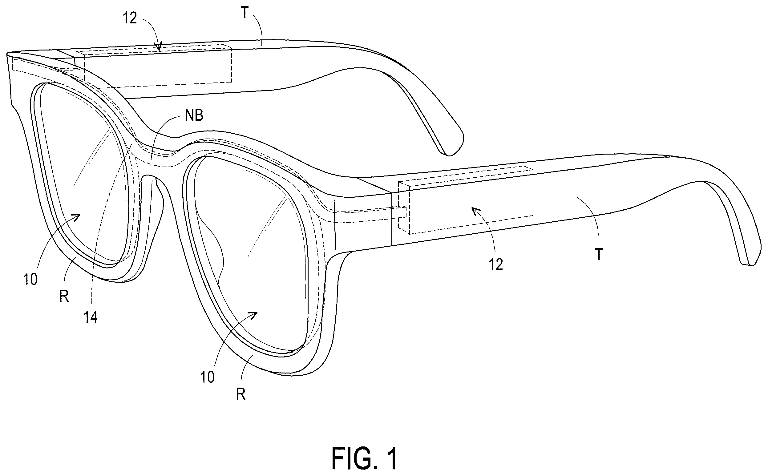
is a schematic view of an electronic device according to an embodiment of the disclosure.
is an exploded schematic view of the rims, optical adjustment structures and a nose bridge in .
A through C are schematic views of the optical adjustment structures in .
A through C , and are schematic views of electronic devices according to various embodiments of the disclosure.
A and A are schematic views of signals applied to the first electrode layer in A through C .
B and B are schematic views of signals applied to the second electrode layer in A through C .
DETAILED DESCRIPTION OF DISCLOSED EMBODIMENTS
References of the exemplary embodiments of the disclosure are to be made in detail. Examples of the exemplary embodiments are illustrated in the drawings. If applicable, the same reference numerals in the drawings and the descriptions indicate the same or similar parts.
Certain terms may be used throughout the disclosure and the appended patent claims to refer to specific elements. It should be understood by those of ordinary skill in the art that electronic device manufacturers may refer to the same element by different names. The disclosure does not intend to distinguish between elements that have the same function but have different names. In the following description and patent claims, words such as “comprising” and “including” are open-ended words, so they should be interpreted as meaning “including but not limited to . . . ”.
In the disclosure, wordings used to indicate directions, such as “up,” “down,” “front,” “back,” “left,” and “right,” merely refer to directions in the accompanying drawings. Therefore, the directional wordings are used to illustrate rather than limit the disclosure. In the accompanying drawings, the drawings illustrate the general features of the methods, structures, and/or materials used in the particular embodiments. However, the drawings shall not be interpreted as defining or limiting the scope or nature covered by the embodiments. For example, the relative sizes, thicknesses, and locations of the layers, regions, and/or structures may be reduced or enlarged for clarity.
A structure (or layer, element, substrate) described in this disclosure is located on/above another structure (or layer, element, substrate), may indicate that the two structures are adjacent and directly connected, or may indicate that the two structures are adjacent but not directly connected. Indirect connection means that there is at least one intermediate structure (or intermediate layer, intermediate element, intermediate substrate, intermediate spacer) between the two structures, the lower surface of one structure is adjacent to or directly connected to the upper surface of the intermediate structure, and the upper surface of another structure is adjacent to or directly connected to the lower surface of the intermediate structure. The intermediate structure may be composed of a single-layer or multi-layer physical structure or a non-physical structure, which is not limited thereto. In the disclosure, when a certain structure is disposed “on” other structures, it may mean that a certain structure is “directly” on other structures, or it means that a certain structure is “indirectly” on other structures, that is, at least one structure is sandwiched between a certain structure and other structures.
The terms such as “first”, “second”, etc. used in the description and the patent claims are used to modify elements, which do not imply and represent that the (or these) elements have any previous ordinal numbers, and also does not represent the order of a certain element and another element, or the order of the manufacturing method. The use of these ordinal numbers is to only clearly distinguish an element with a certain name from another element with the same name. The same terms may not be used in the patent claims and the description, and accordingly, the first component in the description may be the second component in the patent claims.
The coupling described in the disclosure may refer to direct electrical connection or indirect electrical connection. In the case of a direct electrical connection, the end points of two elements on a circuit directly connect to each other, or connect to each other through a conductive wire. In the case of indirect electrical connection, a switch, a diode, a capacitor, an inductor, a resistor, other suitable elements, or a combination thereof, but not limited therein, is between the end points of two elements on a circuit.
In the disclosure, the thickness, length, and width may be measured by adopting a measurement method such as an optical microscope (OM), and the thickness or width may be measured from a cross-sectional image in an electronic microscope, but not limited thereto. In addition, any two values or directions used for comparison may have certain errors. In addition, the terms “about”, “equal to”, “equal” or “same”, “substantially” or “generally” are interpreted as within 20% of a given value or range, or interpreted as within 10%, 5%, 3%, 2%, 1%, or 0.5% of the given value or range. Furthermore, the terms “a given range is from a first value to a second value”, “a given range is within a range from the first value to the second value” means that the given range includes the first value, the second value, and other values in between. If a first direction is perpendicular to a second direction, an angle between the first direction and the second direction may be between 80 degrees and 100 degrees; if the first direction is parallel to the second direction, an angle between the first direction and the second direction may be between 0 degrees and 10 degrees.
It should be noted that, in the following embodiments, the features in several different embodiments may be replaced, reorganized, and mixed to complete other embodiments without departing from the spirit of the disclosure. As long as the features of the various embodiments do not violate the spirit of the disclosure or conflict with one another, they may be mixed and matched arbitrarily.
Unless otherwise defined, all terms (including technical and scientific terms) used herein have the same meaning as commonly understood by one of ordinary skill in the art to which this disclosure belongs. It is understood that these terms, such as those defined in commonly used dictionaries, should be interpreted as having meanings consistent with the relevant art and the background or context of the disclosure, and should not be interpreted in an idealized or overly formal manner, unless otherwise defined in the embodiments of the disclosure.
In the disclosure, an electronic device may include a vision correction device, a display device, a backlight device, an antenna device, a sensing/detecting device, or a tiled device, but is not limited thereto. The electronic device may be a bendable or flexible electronic device. The vision correction device may be a device with variable focal distance to achieve myopia correction, presbyopia correction, amblyopia correction and/or astigmatism correction, but is not limited thereto. The display device may be a non-self-luminous display device or a self-luminous display device. The antenna device may be a liquid crystal antenna device or a non-liquid crystal antenna device, and the sensing/detecting device may be a device for sensing capacitance, light, heat or ultrasonic waves, but not limited thereto. In the disclosure, an electronic device may include electronic elements, and the electronic elements may include passive elements and active elements, such as a capacitor, a resistor, an inductor, a diode, a transistor, and the like. The diode may include a light emitting diode or a photodiode. The light emitting diode may include, for example, an organic light emitting diode (OLED), a mini light emitting diode (mini LED), a micro light emitting diode (micro LED), or a quantum dot light emitting diode (quantum dot LED), but not limited thereto. The tiled device may be, for example, a tiled display device or a tiled antenna device, but not limited thereto. It should be noted that, the electronic device may be any arrangement and combination of the foregoing, but not limited thereto. In addition, the shape of the electronic device may be rectangular, circular, polygonal, a shape with curved edges, or other suitable shapes. The electronic device may have a peripheral system such as a driving system, a control system, a light source system, and the like to support a display device, an antenna device, a wearable device (e.g., including augmented reality or virtual reality), an in-vehicle device (e.g., including car windshields), or a tiled device. Hereinafter, the vision correction device is used as the electronic device to illustrate the disclosure, but the disclosure is not limited thereto.
is a schematic view of an electronic device according to an embodiment of the disclosure. is an exploded schematic view of the rims, optical adjustment structures and a nose bridge in . A through C are schematic views of the optical adjustment structures in . A through C , and are schematic views of electronic devices according to various embodiments of the disclosure, wherein A and A are cross-sectional views respectively corresponding to the line A-A′ in B and B . A and A are schematic views of signals applied to the first electrode layer in A through C . B and B are schematic views of signals applied to the second electrode layer in A through C . In the embodiments shown in through B , the technical solutions provided by the different embodiments hereinafter may be replaced, combined, or mixed with one another, so as to constitute another embodiment without violating the spirit of the disclosure.
Referring to , an electronic device 1 may be glasses for vision correction. Vision correction may include myopia, presbyopia and/or astigmatism correction, but not limited thereto. The electronic device 1 may include optical adjustment structures 10 respectively mounted in rims R of the glasses to perform vision correction for the wearer of the glasses. In some embodiments, the optical adjustment structures 10 may have electrically controllable focal distances, and the electronic device 1 further includes at least one circuit module 12 disposed in at least one of the two temples T of the glasses to provide power and drive functions. The electronic device 1 may also include at least one signal connection element 14 disposed in the glasses (e.g., in the nose bridge NB of the glasses, in the temple T of the glasses, and/or in the any part of the glasses) to electrically connect the optical adjustment structures 10 with the at least one controller 12 for signal and/or power transmission.
In some embodiments, as shown in , the rims R include front rims R 1 and rear rims R 2 , and the nose bridge NB includes a front nose bridge NB 1 connected between the front rims R 1 and a rear bridge NB 2 connected between the rear rims R 2 . However, the construction of the rims R and/or the nose bridge NB may be adjusted according to actual needs. In the disclosure, the rear side of an object refers to the side of the object that faces the wearer of the glasses, and the front side of the object refers to the side of the object opposite to the rear side.
Each of the optical adjustment structure 10 may include a panel assembly 104 , but not limit thereto. In another embodiment, each of the optical adjustment structure 10 may include at least one lens (e.g., a front lens 100 and a rear lens 102 ) and a panel assembly 104 connected to the at least one lens, but not limit thereto. In , two lenses (e.g., the front lens 100 and the rear lens 102 ) respectively located at opposite sides (e.g., front side and rear side) of the panel assembly 104 are illustrated for exemplary explanation purpose. However, the number of the lenses in each of the optical adjustment structure 10 and/or arrangement of the lens/lenses and the panel assembly 104 may be changed according to needs. In addition, the panel assembly 104 may be attached to the at least one lens through an adhesive layer (not shown) or other fixing mechanisms (not shown). The material of the adhesive layer may include optically clear adhesive (OCA), optically clear resin (OCR), double-sided tape, liquid optically clear adhesive (LOCA) or other light-transmitting materials having viscosity. In some embodiments, the optical adjustment structure 10 may be served as lens of the glasses.
In some embodiments, as shown in A , the front lens 100 and the rear lens 102 are respectively a plano-concave lens and a plano-convex lens, and the panel assembly 104 is disposed between the plano-concave lens and the plano-convex lens. The panel assembly 104 may have an optical adjustable region R 104 , wherein the focal distance of the optical adjustable region R 104 may be electrically controllable. In other words, the focal distance of the optical adjustable region R 104 may be changed by an electrically controlled manner. The panel assembly 104 may also have a region R 104 ′ outside the optical adjustable region R 104 , and the diopter of the region R 104 ′ may be fixed.
Specifically, the overall diopter of the region R 104 ′ depends mainly on the front surface SF 104 and the rear surface SR 104 of the panel assembly 104 . When both of the front surface SF 104 and the rear surface SR 104 of the panel assembly 104 are flat (i.e., have infinite radii of curvature), the region R 104 ′ is not used to change the traveling path of light. Similarly, the overall diopter of the optical adjustable region R 104 not only depends on the electrically controlled focal distance but also depends on the front surface SF 104 and the rear surface SR 104 of the panel assembly 104 . When both of the front surface SF 104 and the rear surface SR 104 of the panel assembly 104 are flat, the overall diopter of the optical adjustable region R 104 is determined by the electrically controlled focal distance.
Therefore, when the panel assembly 104 is not driven, both of the optical adjustable region R 104 and the region R 104 ′ let the light pass through without converging or diverging the light, and thus the effective focal distance of the optical adjustment structure 10 (corresponding to both of the optical adjustable region R 104 and the region R 104 ′) depends mainly on the front lens 100 and the rear lens 102 . On the other hand, when the panel assembly 104 is driven, the focal distance of the optical adjustable region R 104 is changed, and the traveling path of the light passing through the optical adjustable region R 104 changes accordingly; in this case, the effective focal length of the optical adjustment structure 10 corresponding to the optical adjustable region R 104 depends on the panel assembly 104 in addition to the front lens 100 and the rear lens 102 , while the effective focal length of the optical adjustment structure 10 corresponding to the region R 104 ′ remains depending mainly on the front lens 100 and the rear lens 102 .
For example, when the panel assembly 104 is not driven, the optical adjustment structure 10 may be used to correct myopia, and when the panel assembly 104 is driven, the optical adjustment structure 10 may be used to correct presbyopia, and in this case, the optical adjustable region R 104 may be located on the lower region of the optical adjustment structure 10 . However, the position/location of the optical adjustable region R 104 in the optical adjustment structure 10 and/or the application of the optical adjustment structure 10 can be changed according to actual needs.
In some embodiments, as shown in B (or C ), the optical adjustment structure 10 includes one lens (e.g., a lens 106 ) and the panel assembly 104 connected to the lens 106 . The lens 106 may be a plano-convex lens, a plano-concave lens, a convex-concave lens, a meniscus lens, a biconvex lens, a biconcave lens or other surface lenses, which may be determined according to practical applications. The panel assembly 104 may be a bendable or flexible lens-form structure attached to a front surface SF of the lens 106 (as shown in B ) or a rear surface SR of the lens 106 (as shown in C ). When both of the front surface SF 104 and the rear surface SR 104 of the panel assembly 104 are surfaces with finite radii of curvature, the effective focal length of the optical adjustment structure 10 further depends on the diopter of the panel assembly 104 when the panel assembly 104 is driven or not driven. In some embodiments, the optical adjustment structure 10 includes a panel assembly 104 , but not limited thereto.
In some embodiments, as shown in A , the panel assembly 104 may include two panels (e.g., a first panel P 1 and a second panel P 2 ) and an adhesive layer AD, wherein the first panel P 1 is attached to the second panel P 2 through the adhesive layer AD. The material of the adhesive layer AD may include optically clear adhesive (OCA), optically clear resin (OCR), double-sided tape, liquid optically clear adhesive (LOCA) or other light-transmitting materials having viscosity. However, the number of the panels in the panel assembly 104 and the fixing manner of the panels are not limited thereto.
Each of the panels (e.g., the first panel P 1 and the second panel P 2 ) in the panel assembly 104 is configured to change the diopter of the panel assembly 104 . In some embodiments, each of the panels (e.g., the first panel P 1 and the second panel P 2 ) is an electronically controlled panel.
For example, the first panel P 1 includes a substrate SUB 1 , a first medium layer M 1 , a first electrode layer E 1 and a second electrode layer E 2 , but not limited thereto. In some embodiments, as shown in A , the first panel P 1 further includes an insulating layer IN 1 , an alignment film AL 1 , a high-impedance film HIF 1 , a substrate SUB 2 , a third electrode layer E 3 and an alignment film AL 2 , but also not limited thereto. One or more elements or layers may be added to or omitted from the first panel P 1 according to actual needs.
The substrate SUB 1 may be a rigid substrate or a flexible substrate. The material of the substrate SUB 1 may include glass, quartz, ceramic, sapphire, polycarbonate (PC), polyimide (PI), polypropylene (PP), polyethylene terephthalate (PET), other suitable materials, or a combination of the foregoing materials, but not limited thereto.
The first medium layer M 1 is disposed on the substrate SUB 1 . For example, the first medium layer M 1 is disposed between the alignment film AL 1 and the alignment film AL 2 . In some embodiments, the first medium layer M 1 is a liquid crystal layer including first liquid crystal molecules LCM 1 , but not limited thereto. The first liquid crystal molecules LCM 1 are tilted according to the rubbing direction (not shown) of the alignment film AL 1 and the alignment film AL 2 when no voltage is applied to the first panel P 1 . In the embodiment shown in A , the rubbing direction of the alignment film AL 1 and the alignment film AL 2 is along direction D 1 , and the first medium layer M 1 includes the first liquid crystal molecules LCM 1 with a first alignment direction (e.g., direction D 1 ); however, the rubbing direction of the alignment film AL 1 and the alignment film AL 2 may be changed according to needs.
The first electrode layer E 1 is disposed between the substrate SUB 1 and the first medium layer M 1 . For example, the first electrode layer E 1 is disposed on the substrate SUB 1 . The first electrode layer E 1 may be a non-patterned transparent conductive layer. Transparent conductive material may include metal oxide (e.g., indium tin oxide), carbon nanotube, graphene, other suitable materials, or a combination thereof, but not limited to.
The insulating layer IN 1 is disposed on the first electrode layer E 1 and is configured to electrically isolated the first electrode layer E 1 from the second electrode layer E 2 . The material of the insulating layer IN 1 may include inorganic insulating material, organic insulating material or a combination thereof, but not limited thereto.
The second electrode layer E 2 is disposed between the first electrode layer E 1 and the first medium layer M 1 . For example, the second electrode layer E 2 is disposed on the insulating layer IN 1 . The second electrode layer E 2 may be a patterned transparent conductive layer. Transparent conductive material may include metal oxide (e.g., indium tin oxide), carbon nanotube, graphene, other suitable materials, or a combination thereof, but not limited thereto. As shown in A and B , the edge (see the dash line in B ) of the optical adjustable region R 104 may be defined by the inner edge of the second electrode layer E 2 .
The alignment film AL 1 is disposed between the second electrode layer E 2 and the first medium layer M 1 . For example, the alignment film AL 1 is disposed on the high-impedance film HIF 1 . The material of the alignment film AL 1 may include polymer, but not limited thereto.
The high-impedance film HIF 1 is disposed between the alignment film AL 1 and the second electrode layer E 2 . For example, the high-impedance film HIF 1 is disposed on the insulating layer IN 1 and the second electrode layer E 2 . The high-impedance film HIF 1 may be a non-patterned conductive layer with a high surface impedance. For example, a surface impedance of the high-impedance film HIF 1 is 10 5 Ω/□ to 10 10 Ω/□, but not limited thereto. The material of the high-impedance film HIF 1 may include conductive polymer, transparent conductive oxide, metal, carbon nanotube, graphene, or a combination thereof, and the high-impedance film HIF 1 may be disposed on the insulating layer IN 1 and the second electrode layer E 2 through coating, but not limited thereto.
The substrate SUB 2 is opposite to the substrate SUB 1 . In other words, the substrate SUB 2 is overlapped with the substrate SUB 1 along a thickness direction (e.g., direction D 3 ) of the first panel P 1 . The substrate SUB 2 may also be a rigid substrate or a flexible substrate. Material of the substrate SUB 2 may refer to the material of the substrate SUB 1 , which will not be repeated here.
The third electrode layer E 3 is disposed on the substrate SUB 2 and is disposed between the first medium layer M 1 and the substrate SUB 2 . The third electrode layer E 3 may be a non-patterned transparent conductive layer. Transparent conductive material may include metal oxide (e.g., indium tin oxide), carbon nanotube, graphene, other suitable materials, or a combination thereof, but not limited to.
The alignment film AL 2 is disposed on the third electrode layer E 3 and is disposed between the first medium layer M 1 and the third electrode layer E 3 . The material of the alignment film AL 2 may include polymer, but not limited thereto.
The second panel P 2 may have a similar structure to the first panel P 1 . For example, the second panel P 2 may include a substrate SUB 3 , a second medium layer M 2 , a fourth electrode layer E 4 , a fifth electrode layer E 5 , an insulating layer IN 2 , an alignment film AL 3 , a high-impedance film HIF 2 , a substrate SUB 4 , a sixth electrode layer E 6 and an alignment film AL 4 , but not limited thereto. One or more elements or layers may be added to or omitted from the second panel P 2 according to actual needs. The material and/or the disposition relationship of the layers above may refer to the description of the substrate SUB 1 , the first medium layer M 1 , the first electrode layer E 1 , the second electrode layer E 2 , the insulating layer IN 1 , the alignment film AL 1 , the high-impedance film HIF 1 , the substrate SUB 2 , the third electrode layer E 3 and the alignment film AL 2 , which will not be repeated here.
The main difference between the first panel P 1 and the second panel P 2 is that the second medium layer M 2 includes second liquid crystal molecules LCM 2 with a second alignment direction (e.g., direction D 2 ) different from the first alignment direction (e.g., direction D 1 ). Specifically, the second liquid crystal molecules LCM 2 are tilted according to the rubbing direction (not shown) of the alignment film AL 3 and the alignment film AL 4 when no voltage is applied to the second panel P 2 . In the embodiment as shown in A , the rubbing direction of the alignment film AL 3 and the alignment film AL 4 is along direction D 2 , and the second medium layer M 2 includes the second liquid crystal molecules LCM 2 with the second alignment direction (e.g., direction D 2 ); however, the rubbing direction of the alignment film AL 3 and the alignment film AL 4 may be changed according to needs.
In some embodiments, the first alignment direction (e.g., direction D 1 ) is perpendicular to the second alignment direction (e.g., direction D 2 ) to respectively control the diopters of the light waves whose polarization directions are perpendicular to each other, in this way, the electronic device can be polarizer-free, but not limited thereto.
When the diopter of the optical adjustable region R 104 is to be adjusted, a first voltage V 1 is applied to the first electrode layer E 1 , a second voltage V 2 is applied to the second electrode layer E 2 , and the first voltage V 1 is different from the second voltage V 2 . The first voltage V 1 is the absolute of the voltage difference between the first electrode layer E 1 and the third electrode layer E 3 , and the second voltage V 2 is the absolute of the voltage difference between the second electrode layer E 2 and the third electrode layer E 3 . The first voltage V 1 may be larger or smaller than the second voltage V 2 . In A through B , high voltage VH served as the first voltage V 1 and low voltage VL served as the second voltage V 2 are illustrated for exemplary explanation purpose. However, in some embodiments, the second voltage V 2 may be the high voltage VH, and the first voltage V 1 may be the low voltage VL. As shown in A and B , the first voltage V 1 (high voltage VH) and the second voltage V 2 (low voltage VL) may be in the form of AC voltages. In A and B , “GND” refers to a ground voltage, to which the third electrode layer E 3 is connected, for example; “VH” refers to a positive high voltage, during which the voltage level of the first electrode layer E 1 is greater than that of the third electrode layer E 3 ; “−VH” refers to a negative high voltage, during which the voltage level of the first electrode layer E 1 is lower than that of the third electrode layer E 3 ; “VL” refers to a positive low voltage, during which the voltage level of the second electrode layer E 2 is higher than that of the third electrode layer E 3 ; “−VL” refers to a negative low voltage, during which the voltage level of the second electrode layer E 2 is lower than that of the third electrode layer E 3 . In some embodiments, |VH|≤50 V, and |VL|≤0.5*|VH|, but not limited thereto.
In some embodiments, as shown in A and B , a third voltage V 3 is applied to the first electrode layer E 1 and the second electrode layer E 2 before the first voltage V 1 (e.g., high voltage VH) is applied to the first electrode layer E 1 and the second voltage V 2 (e.g., low voltage VL) is applied to the second electrode layer E 2 . In some embodiments, the first voltage V 1 (e.g., high voltage VH) is greater than the second voltage V 2 (e.g., low voltage VL), the third voltage V 3 is greater than the first voltage V 1 and the second voltage V 2 , and the third voltage V 3 is less than or equal to 2.5 times the first voltage V 1 . For example, the third voltage V 3 is less than 1.5 times the first voltage V 1 , but not limited thereto. By applying a large voltage (the third voltage V 3 ) to the first electrode layer E 1 and the second electrode layer E 2 before applying the first voltage V 1 to the first electrode layer E 1 and applying the second voltage V 2 to the second electrode layer E 2 , the tilting of the first liquid crystal molecules LCM 1 can be accelerated, which helps to increase the zoom speed.
In some embodiments, referring back to A , the first voltage V 1 is also applied to the fourth electrode layer E 4 , and the second voltage V 2 is also applied to the fifth electrode layer E 5 . The first voltage V 1 is the absolute of the voltage difference between the fourth electrode layer E 4 and the sixth electrode layer E 6 , and the second voltage V 2 is the absolute of the voltage difference between the fifth electrode layer E 5 and the sixth electrode layer E 6 . The method of applying voltages to these electrodes can be referred to the description of A through B , which will not be repeated here.
When the voltage difference (e.g., |V 1 −V 2 |) is applied to each of the first panel P 1 and the second panel P 2 , the first liquid crystal molecules LCM 1 and the second liquid crystal molecules LCM 2 tilt according to the electric fields respectively across the first medium layer M 1 and the second medium layer M 2 , and thus the diopter of the optical adjustable region R 104 is changed.
By arranging the high-impedance film (e.g., the high-impedance film HIF 1 and/or the high-impedance film HIF 2 ) between the electrode layer and the medium layer (e.g., the second electrode layer E 2 and the first medium layer M 1 and/or the fifth electrode layer E 5 and the second medium layer M 2 ), the electric field variation near the boundary between the optical adjustable region R 104 and the region R 104 ′ become a gradual variation from a steep variation, and the liquid crystal molecules (including the first liquid crystal molecules LCM 1 and the second liquid crystal molecules LCM 2 ) are gradually tilted near the boundary between the optical adjustable region R 104 and the region R 104 ′ accordingly. In this way, the magnification of the image seen by the user near the boundary between the optical adjustable region R 104 and the region R 104 ′ is gradually changed, so that better image quality can be provided.
In some embodiments, as shown in , the optical adjustable region R 104 of the panel assembly 104 serves as a convex lens when the first voltage V 1 is smaller than the second voltage V 2 (e.g., when the low voltage VL in B or B is served as the first voltage V 1 , and the high voltage VH in A or A is served as the second voltage V 2 ). In some embodiments, as shown in , the optical adjustable region R 104 of the panel assembly 104 serves as a concave lens when the first voltage V 1 is larger than the second voltage V 2 (e.g., when the high voltage VH in A or A is served as the first voltage V 1 , and the low voltage VL in B or B is served as the second voltage V 2 ), but not limited thereto. By adjusting the applied voltages (e.g., the first voltage V 1 and/or the second voltage V 2 ) or the voltage difference (e.g., |V 1 −V 2 |), different electric fields can be generated, and thus different focal distances of the optical adjustable region R 104 can be generated. For example, the focal distance of the optical adjustable region R 104 can be switched between far, medium and near sides, and the electronic device using the panel assembly 104 may provide continuous zoom function accordingly. Moreover, the combination of the panel assembly 104 and the general lens(s) (e.g., the front lens 100 and the rear lens 102 shown in A or the les 106 shown in B or C ) helps to improve the problem of the apparent visibility of the Fresnel optical adjustment structure, and thus the display quality can be improved. By changing the voltage difference between the first electrode layer E 1 and the second electrode layer E 2 , the tilting angle of the first liquid crystal molecules LCM 1 can be changed, so that the refractive index of the first panel P 1 can be changed correspondingly, and thus achieving the dimming effect.
In A , the first panel P 1 and the second panel P 2 presenting a mirror-symmetrical structure with the adhesive layer AD as the axis of symmetry is illustrated for exemplary explanation purpose. However, in some embodiments, at least one of the first panel P 1 and the second panel P 2 may be arranged upside down, and/or positions of the first panel P 1 and the second panel P 2 can be switched. The following embodiments can be changed accordingly, and will not be repeated below.
In A , the first electrode layer E 1 and the fourth electrode layer E 4 applied with the same voltage (e.g., the first voltage V 1 ) and the second electrode layer E 2 and the fifth electrode layer E 5 applied with the same voltage (e.g., the second voltage V 2 ) are illustrated for exemplary explanation purpose. However, the voltage applied to the first electrode layer E 1 may be different from the voltage applied to the fourth electrode layer E 4 , and the voltage applied to the second electrode layer E 2 may be different from the voltage applied to the fifth electrode layer E 5 , while the voltage difference applied to the first panel P 1 and the second panel P 2 may be the same. However, deviations may exist in voltage differences between different panels due to process variation. The following embodiments can be changed accordingly, and will not be repeated below.
In A , two panels (the first panel P 1 and the second panel P 2 ) are illustrated for exemplary explanation purpose. However, the number of the panels in the panel assembly 104 may be changed according to needs. For example, the number of the panels in the panel assembly 104 may be increased to increase the zoom range. As exemplary explanation, if the zoom range of the two panels is 0 degrees to 50 degrees, the zoom range of the four panels is 0 degrees to 100 degrees, and so on. Although not shown, the electronic device may include a plurality of the first panels and a plurality of the second panels overlapped with the plurality of first panels. The plurality of first panels and the plurality of the second panels may be alternately arranged along the direction D 3 , but not limited thereto. The details of the signal supply of the plurality of first panels P 1 and the plurality of second panels P 2 can be referred to above, and will not be repeated here.
In some embodiments, cell gaps (e.g., a cell gap CG 1 and a cell gap CG 2 ) of the panels may be increased to increase the zoom range. For example, the cell gaps can be increased by 1.5, 2, 3 times, etc., so that the zoom range can be increased by 1.5, 2, 3 times, etc., but not limited thereto.
In some embodiments, as shown in A , the first panel P 1 further includes a sealant SL 1 that surrounds the first medium layer M 1 and an adhesive layer AD 1 that surrounds the sealant SL 1 . The material of the adhesive layer AD 1 may refer to the material of the adhesive layer AD, and will not be repeated here. Similarly, the second panel P 2 may further include a sealant SL 2 that surrounds the second medium layer M 2 and an adhesive layer AD 2 that surrounds the sealant SL 2 . The material of the adhesive layer AD 2 may refer to the material of the adhesive layer AD, and will not be repeated here.
In some embodiments, as shown in , the electronic device further includes an electrochromic layer ECL to provide sunglasses function. The first panel P 1 may be disposed between the electrochromic layer EL and the second panel P 2 . However, the arrangement relationship between the electrochromic layer ECL, the first panel P 1 and the second panel P 2 may be changed according to needs. For example, the second panel P 2 may be disposed between the electrochromic layer ECL and the first panel P 1 , but not limited thereto.
In some embodiments, as shown in , the electronic device further includes a substrate SUB 3 , a seventh electrode layer E 7 , an electrolyte layer ETL, an ion storage layer ISL and an eighth electrode layer E 8 , but not limited thereto. For example, the electronic device may further include a substrate (not shown; e.g., a fourth substrate) between the eighth electrode layer E 8 and the substrate SUB 2 , but not limited thereto.
The substrate SUB 3 and the fourth substrate (if existed) are overlapped with the substrate SUB 1 along the direction D 3 . Materials of the substrate SUB 3 and the fourth substrate may refer to the material of the substrate SUB 1 , which will not be repeated here.
The seventh electrode layer E 7 is disposed between the electrochromic layer ECL and the substrate SUB 3 . The seventh electrode layer E 7 may be a non-patterned transparent conductive layer. Transparent conductive material may include metal oxide (e.g., indium tin oxide), carbon nanotube, graphene, other suitable materials, or a combination thereof, but not limited to.
The electrochromic layer ECL is disposed between the electrolyte layer ETL and the seventh electrode layer E 7 , the electrolyte layer ETL is disposed between the electrochromic layer ECL and the ion storage layer ISL, and the eighth electrode layer E 8 is disposed between the ion storage layer ISL and the substrate SUB 2 . The eighth electrode layer E 8 may be a non-patterned transparent conductive layer. Transparent conductive material may include metal oxide (e.g., indium tin oxide), carbon nanotube, graphene, other suitable materials, or a combination thereof, but not limited to.
When a voltage V is applied to the eighth electrode layer E 8 , the electrochromic layer ECL is switched from a transparent state to a colored state (e.g., a dark state). On the other hand, when no voltage is applied to the eighth electrode layer E 8 , the electrochromic layer ECL is switched from the colored state back to the transparent state. The voltage V refers to the absolute of the voltage difference between the seventh electrode layer E 7 and the eighth electrode layer E 8 .
The electronic device of any embodiment of the present disclosure can provide sunglasses function by disposing the electrochromic layer ECL and/or other layers (e.g., the substrate SUB 3 , the seventh electrode layer E 7 , the electrolyte layer ETL, the ion storage layer ISL, the eighth electrode layer E 8 and/or the fourth substrate) described in , which will not be repeated below.
In some embodiments, as shown in , a panel assembly 104 ′ of an electronic device 1 ′ includes only one panel (e.g., the first panel P 1 ) and a polarizer PL overlapped with the first panel P 1 . The polarizer PL may be attached to a front surface SFP 1 or a rear surface SRP 1 of the first panel P 1 through an adhesive layer (not shown) or other fixing mechanisms (not shown). The polarizer PL is, for example, an absorptive polarizer, but not limited to. The second panel P 2 described above can be omitted by filtering (e.g., absorbing) the light whose polarization direction is perpendicular to the first alignment direction through the polarizer PL.
In other embodiments not shown, the electronic device 1 ′ further includes a plano-concave lens (e.g., the front lens 100 shown in A ) and a plano-convex lens (e.g., the rear lens 102 shown in A ), wherein the first panel P 1 and the polarizer PL are disposed between the plano-concave lens and the plano-convex lens. Alternatively, the electronic device 1 ′ may further include the lens 106 shown in B or C , and the panel assembly 104 ′ may be attached to the front surface SF 106 or the rear surface SR 106 of the lens 106 . In some embodiments, the polarizer PL can be positioned on the front surface or the rear surface of the plano-concave lens, or the front surface or the rear surface of the plano-convex lens, but not limited to.
In other embodiments not shown, the first panel P 1 of the electronic device 1 ′ further includes the sealant SL 1 and the adhesive layer AD 1 shown in A . In other embodiments not shown, the electronic device 1 ′ further includes the electrochromic layer ECL (shown in ) overlapped with the first panel P 1 and the polarizer PL to provide sunglasses function. In other embodiments not shown, the electronic device 1 ′ includes a plurality of the first panels P 1 overlapped with each other along the direction D 3 to increase the zoom range. In other embodiments not shown, the cell gap CG 1 of the first panel P 1 may be increased to increase the zoom range.
In some embodiments, as shown in A , the electronic device 1 (or the electronic device 1 ′ I ) includes one circuit module 12 and a plurality of signal connection elements (e.g., FPC, trigger lines or combination thereof) 14 . In some embodiments, the circuit module 12 includes a touch sensor 120 , a power supply unit (e.g., a battery) 122 and a circuit board 124 , but not limited to. The touch sensor 120 is electrically connected to the circuit board 124 through at least one of the plurality of signal connection elements 14 . The power supply unit 122 is electrically connected to the circuit board 124 through at least one of the plurality of signal connection elements 14 . Each of the optical adjustment structure 10 is electrically connected to the circuit board 124 through at least one of the plurality of signal connection elements 14 . In some embodiments, the plurality of signal connection elements 14 are disposed in different parts (e.g., the temples T and/or rims R shown in ) of the glasses. The panel assembly in the optical adjustment structure 10 can be driven by touching the touch sensor 120 , and the touch sensor 120 can adjust different diopters in segments. In A , the circuit module 12 on the left eye side of the glasses is illustrated for exemplary explanation purpose. However, the relative disposition between the optical adjustment structure 10 and the circuit module 12 may be changed according to needs. For example, the circuit module 12 may be on the right eye side of the glasses, but not limited to.
In some embodiments, as shown in B , the electronic device 1 (or the electronic device 1 ′I ) includes two circuit modules (e.g., the circuit module 12 and a circuit module 12 ′) and a plurality of signal connection elements 14 . The circuit module 12 is, for example, on the right eye side of the glasses and electrically connected to the panel assembly in optical adjustment structure 10 on the right eye side of the glasses. The circuit module 12 ′ is, for example, on the left eye side of the glasses and electrically connected to the panel assembly in optical adjustment structure 10 on the left eye side of the glasses. The circuit module 12 ′ may include the power supply unit 122 and the circuit board 124 . The circuit board 124 of the circuit module 12 and the circuit board 124 of the circuit module 12 ′ are electrically connected through at least one of the plurality of signal connection elements 14 . The circuit board 124 of the circuit module 12 may be a main circuit board, and the circuit board 124 of the circuit module 12 ′ may be an auxiliary circuit board. After touching the touch sensor 120 , the driving circuits (not shown) in the main and auxiliary circuit boards can be triggered at the same time, and the touch sensor 120 can adjust different diopters in segments. In other embodiments not shown, positions of the main circuit board and the auxiliary circuit board may be interchanged.
In some embodiments, as shown in C , the electronic device 1 (or the electronic device 1 ′ I ) includes two circuit modules 12 and a plurality of signal connection elements 14 . In this way, the optical adjustment structure 10 can be individually controlled. Specifically, the panel assembly in the optical adjustment structure 10 on the right eye side of the glasses can be driven by touching the touch sensor 120 on the right eye side of the glasses, and the panel assembly in the optical adjustment structure 10 on the left eye side of the glasses can be driven by touching the touch sensor 120 on the left eye side of the glasses.
To sum up, in the embodiments of the disclosure, by adjusting the applied voltages (e.g., the first voltage V 1 and/or the second voltage V 2 ) or the voltage difference (e.g., |V 1 −V 2 |), different electric fields can be generated, and thus different focal distances can be generated, and the electronic device may provide continuous zoom function accordingly. In some embodiments, the problem of the apparent visibility of the Fresnel optical adjustment structure can be improved by using general lens(s) in combination of a panel assembly, and thus the display quality can be improved accordingly.
The foregoing embodiments are only used to illustrate the technical solutions of the disclosure, but not to limit the disclosure; although the disclosure has been described in detail with reference to the foregoing embodiments, persons of ordinary skill in the art should understand that the technical solutions described in the foregoing embodiments may still be modified, or parts or all of the technical features thereof may be equivalently replaced; however, these modifications or substitutions do not deviate the essence of the corresponding technical solutions from the scope of the technical solutions of the embodiments of the disclosure.
Although the embodiments of the disclosure and the advantages thereof have been disclosed above, it should be understood that any person with ordinary skill in the art may make changes, substitutions, and modifications without departing from the spirit and scope of the disclosure, and the features of the various embodiments may be arbitrarily mixed and replaced with one another to form other new embodiments. In addition, the protection scope of the disclosure is not limited to the processes, machines, manufactures, compositions of the matter, devices, methods, and steps in the specific embodiments described in the specification. It is understood that processes, machines, manufactures, compositions of matter, devices, methods, and steps developed in the present or in the future may be used in accordance with the disclosure as long as they may implement substantially the same functions or achieve substantially the same results in the embodiments described herein. Therefore, the protection scope of the disclosure includes the above-mentioned processes, machines, manufactures, compositions of matter, devices, methods, and steps. In addition, each of the claims constitutes a separate embodiment, and the protection scope of the disclosure also includes each of the combinations of the claims and the embodiments. The protection scope of the disclosure shall be determined by the appended patent claims.
Figures (13)
Citations
This patent cites (6)
- US10802374
- US2017/0323615
- US2020/0209668
- US2021/0247627
- US2022/0026742
- USI709790