Abstract
An electronic device includes a light emitting device, and the light emitting device emits a light towards a light-emitting direction. The light emitting device includes a substrate, a first light emitting component and a second light emitting component. The first light emitting component is disposed on the substrate, and the first light emitting component includes a first light emitting unit and a first light controlling unit, wherein the first light controlling unit is disposed on the first light emitting unit in the light-emitting direction, and the first light emitting component provides a first light with a first light type. The second light emitting component is disposed on the substrate, and the second light emitting component includes a second light emitting unit, wherein the second light emitting component provides a second light with a second light type, and the first light type is different from the second light type.
Claims (10)
1. An electronic device, comprising a light emitting device, wherein the light emitting device emits a light towards a light-emitting direction, and the light emitting device comprises: a substrate; a plurality of light controlling units disposed on the substrate; a first light emitting component disposed on the substrate, the first light emitting component comprising a first light emitting unit and a first light controlling unit, wherein the first light controlling unit disposed on a side of the first light emitting unit in a side direction of the first light emitting unit, the side direction of the first light emitting unit is not parallel to the light-emitting direction, the plurality of light controlling units comprise the first light controlling unit, and the first light emitting component provides a first light with a first light type; and a second light emitting component disposed on the substrate, the second light emitting component comprising a second light emitting unit, wherein the second light emitting component provides a second light with a second light type, and the first light type is different from the second light type; wherein a reference light controlling unit is one light controlling unit among the plurality of light controlling units closest to the second light emitting unit, the first light emitting component or the second light emitting component comprises the reference light controlling unit, and a first distance between the first light emitting unit and the first light controlling unit is different from a second distance between the second light emitting unit and the reference light controlling unit.
Show 9 dependent claims
2. The electronic device according to claim 1 , wherein the reference light controlling unit is the first light controlling unit.
3. The electronic device according to claim 1 , wherein the second light emitting component comprises a second light controlling unit, the second light controlling unit is disposed on a side of the second light emitting unit in a side direction of the second light emitting unit, the side direction of the second light emitting unit is not parallel to the light-emitting direction, and the reference light controlling unit is the second light controlling unit.
4. The electronic device according to claim 3 , wherein a first height of the first light controlling unit is greater than a second height of the second light controlling unit in the light-emitting direction.
5. The electronic device according to claim 1 , wherein the first light controlling unit comprises a light absorbing material.
6. The electronic device according to claim 1 , wherein the first light controlling unit surrounds the first light emitting unit.
7. The electronic device according to claim 1 , wherein the first light of the first light emitting component has a first view angle, the second light of the second light emitting component has a second view angle, and the first view angle is less than the second view angle.
8. The electronic device according to claim 1 , wherein the first light emitting unit is turned on and the second light emitting unit is turned off in a first lighting mode.
9. The electronic device according to claim 1 , wherein the second light emitting unit is turned on and the first light emitting unit is turned off in a second lighting mode.
10. The electronic device according to claim 1 , wherein the first light controlling unit comprises two strip structures.
Full Description
Show full text →
BACKGROUND OF THE DISCLOSURE
1. Field of the Disclosure
The present disclosure relates to an electronic device, and more particularly to an electronic device with a function of privacy screen.
2. Description of the Prior Art
As the evolution and development of electronic devices, the electronic devices have become an indispensable item. The electronic devices such as light emitting devices (or display devices) provide more convenient information transmission or image display. However, in order to enhance the privacy when viewing the electronic device and/or to prevent specific persons from viewing the electronic device for increasing safety, the electronic device needs a design which is capable of controlling the light route, so as to make the electronic device have a function of privacy screen.
SUMMARY OF THE DISCLOSURE
According to an embodiment, the present disclosure provides an electronic device including a light emitting device, wherein the light emitting device emits a light towards a light-emitting direction. The light emitting device includes a substrate, a first light emitting component and a second light emitting component. The first light emitting component is disposed on the substrate, and the first light emitting component includes a first light emitting unit and a first light controlling unit, wherein the first light controlling unit is disposed on the first light emitting unit in the light-emitting direction, and the first light emitting component provides a first light with a first light type. The second light emitting component is disposed on the substrate, and the second light emitting component includes a second light emitting unit, wherein the second light emitting component provides a second light with a second light type, and the first light type is different from the second light type.
According to another embodiment, the present disclosure provides an electronic device including a light emitting device, wherein the light emitting device emits a light towards a light-emitting direction. The light emitting device includes a substrate, a plurality of light controlling units, a first light emitting component and a second light emitting component. The light controlling units are disposed on the substrate. The first light emitting component is disposed on the substrate, and the first light emitting component includes a first light emitting unit and a first light controlling unit, wherein the first light controlling unit disposed on a side of the first light emitting unit in a side direction of the first light emitting unit, the side direction of the first light emitting unit is not parallel to the light-emitting direction, the light controlling units include the first light controlling unit, and the first light emitting component provides a first light with a first light type. The second light emitting component is disposed on the substrate, and the second light emitting component includes a second light emitting unit, wherein the second light emitting component provides a second light with a second light type, and the first light type is different from the second light type. A reference light controlling unit is one light controlling unit among the plurality of light controlling units closest to the second light emitting unit, the first light emitting component or the second light emitting component includes the reference light controlling unit, and a first distance between the first light emitting unit and the first light controlling unit is different from a second distance between the second light emitting unit and the reference light controlling unit.
BRIEF DESCRIPTION OF THE DRAWINGS
is a schematic diagram showing a top view of an electronic device according to a first embodiment of the present disclosure.
is a schematic diagram showing cross-sectional views of exemplary designs of light emitting components according to the present disclosure.
is a schematic diagram showing a cross-sectional view of a light emitting device in a first lighting mode and a second lighting mode according to a first embodiment of the present disclosure.
is a schematic diagram showing view angles of a light emitting device in a first lighting mode and a second lighting mode according to a first embodiment of the present disclosure.
is a schematic diagram showing a cross-sectional view of an electronic device according to an embodiment of the present disclosure.
is a schematic diagram showing a top view of an electronic device according to a second embodiment of the present disclosure.
is a schematic diagram showing a top view of an electronic device according to a third embodiment of the present disclosure.
is a schematic diagram showing cross-sectional views of exemplary designs of light emitting components according to the present disclosure.
is a schematic diagram showing a top view of an electronic device according to a fourth embodiment of the present disclosure.
is a schematic diagram showing a top view of an electronic device according to a fifth embodiment of the present disclosure.
is a schematic diagram showing a top view of an electronic device according to a sixth embodiment of the present disclosure.
is a schematic diagram showing a top view of an electronic device according to a seventh embodiment of the present disclosure.
is a schematic diagram showing a top view of an electronic device according to an eighth embodiment of the present disclosure.
DETAILED DESCRIPTION
The present disclosure may be understood by reference to the following detailed description, taken in conjunction with the drawings as described below. It is noted that, for purposes of illustrative clarity and being easily understood by the readers, various drawings of this disclosure show a portion of an electronic device in this disclosure, and certain elements in various drawings may not be drawn to scale. In addition, the number and dimension of each device shown in drawings are only illustrative and are not intended to limit the scope of the present disclosure.
Certain terms are used throughout the description and following claims to refer to particular components. As one skilled in the art will understand, electronic equipment manufacturers may refer to a component by different names. This document does not intend to distinguish between components that differ in name but not function.
In the following description and in the claims, the terms “include”, “comprise” and “have” are used in an open-ended fashion, and thus should be interpreted to mean “include, but not limited to . . . ”. Thus, when the terms “include”, “comprise” and/or “have” are used in the description of the present disclosure, the corresponding features, areas, steps, operations and/or components would be pointed to existence, but not limited to the existence of one or a plurality of the corresponding features, areas, steps, operations and/or components.
The directional terms used throughout the description and following claims, such as: “on”, “up”, “above”, “down”, “below”, “front”, “rear”, “back”, “left”, “right”, etc., are only directions referring to the drawings. Therefore, the directional terms are used for explaining and not used for limiting the present disclosure. Regarding the drawings, the drawings show the general characteristics of methods, structures, and/or materials used in specific embodiments. However, the drawings should not be construed as defining or limiting the scope or properties encompassed by these embodiments. For example, for clarity, the relative size, thickness, and position of each layer, each area, and/or each structure may be reduced or enlarged.
When the corresponding component such as layer or area is referred to “on another component”, it may be directly on this another component, or other component(s) may exist between them. On the other hand, when the component is referred to “directly on another component (or the variant thereof)”, any component does not exist between them. Furthermore, when the corresponding component is referred to “on another component”, the corresponding component and the another component have a disposition relationship along a top-view/vertical direction, the corresponding component may be below or above the another component, and the disposition relationship along the top-view/vertical direction are determined by an orientation of the device.
It will be understood that when a component or layer is referred to as being “connected to” another component or layer, it can be directly connected to this another component or layer, or intervening components or layers may be presented. In contrast, when a component is referred to as being “directly connected to” another component or layer, there are no intervening components or layers presented. In addition, when the component is referred to “be coupled to/with another component (or the variant thereof)”, it may be directly connected to this another component, or may be indirectly connected (such as electrically connected) to this another component through other component(s).
In the description and following claims, the term “horizontal direction” generally means a direction parallel to a horizontal surface, the term “horizontal surface” generally means a surface parallel to a direction X and a direction Y in the drawings, the term “vertical direction” generally means a direction parallel to a direction Z in the drawings, and the direction X, the direction Y and the direction Z are perpendicular to each other (i.e., the horizontal direction is perpendicular to the direction Z). In the description and following claims, the term “top view” generally means a viewing result viewing along the vertical direction. In the description and following claims, the term “cross-sectional view” generally means a viewing result viewing a structure cutting along the vertical direction along the horizontal direction.
In the description and following claims, it should be noted that the term “overlap” means that two elements overlap along the direction Z, and the term “overlap” can be “partially overlap” or “completely overlap” in unspecified circumstances.
The terms “about”, “substantially”, “equal”, or “same” generally mean within ±20% of a given value or range, or mean within ±10%, ±5%, ±3%, ±2%, ±1%, or ±0.5% of a given value or range.
Although terms such as first, second, third, etc., may be used to describe diverse constituent elements, such constituent elements are not limited by the terms. These terms are used only to discriminate a constituent element from other constituent elements in the specification, and these terms have no relation to the manufacturing order of these constituent components. The claims may not use the same terms, but instead may use the terms first, second, third, etc. with respect to the order in which an element is claimed. Accordingly, in the following description, a first constituent element may be a second constituent element in a claim.
It should be noted that the technical features in different embodiments described in the following can be replaced, recombined, or mixed with one another to constitute another embodiment without departing from the spirit of the present disclosure.
In the present disclosure, the electronic device may include a light emitting device, a display device, a backlight device, an antenna device, a sensing device, a tiled device or a combination thereof, but not limited thereto. The light emitting device may be a foldable electronic device, a flexible electronic device or a stretchable electronic device. The display device may be a non-self-luminous type display device or a self-luminous type display device based on requirement(s), and the display device may be a color display device or a monochrome display device based on requirement(s). For example, the display device suitable for the present disclosure may be a liquid crystal display device, an organic light emitting diode (OLED) display device, a mini light emitting diode (mini LED) display device, a micro light emitting diode (micro LED) display device, but not limited thereto. The antenna device may be a liquid-crystal-type antenna device or a non-liquid-crystal-type antenna device, the sensing device may be a device for sensing capacitance, light, thermal or ultrasonic, and the tiled device may be a tiled display device or a tiled antenna device, but not limited thereto. Electronic components of the light emitting device may include passive component(s) and active component(s), such as capacitors, resistors, inductors, diodes and/or transistors. The diode may include a light emitting diode (LED) or a photodiode. The light emitting diode may include an OLED, a mini LED, a micro-LED, a quantum-dot LED (QLED, QDLED), but not limited thereto. The transistor may be a top gate thin film transistor, a bottom gate thin film transistor or a dual gate thin film transistor, but not limited thereto. The light emitting device may include fluorescence material, phosphor material, quantum dot (QD) material or other suitable material based on requirement(s), but not limited thereto. The light emitting device may have a peripheral system (such as a driving system, a control system, a light system, etc.) for supporting the device(s) and component(s) in the light emitting device. A shape of the light emitting device may be a polygon (e.g., a rectangle), a shape having a curved edge (e.g., a circle, an oval) or other suitable shape, but not limited thereto.
In the present disclosure, the light emitting device may have a light-emitting region configured to emit light (e.g., display an image), and the light-emitting region of the light emitting device emits a light towards the light-emitting direction. For example, the light-emitting direction of the present disclosure may be parallel to the direction Z in the drawings, but not limited thereto.
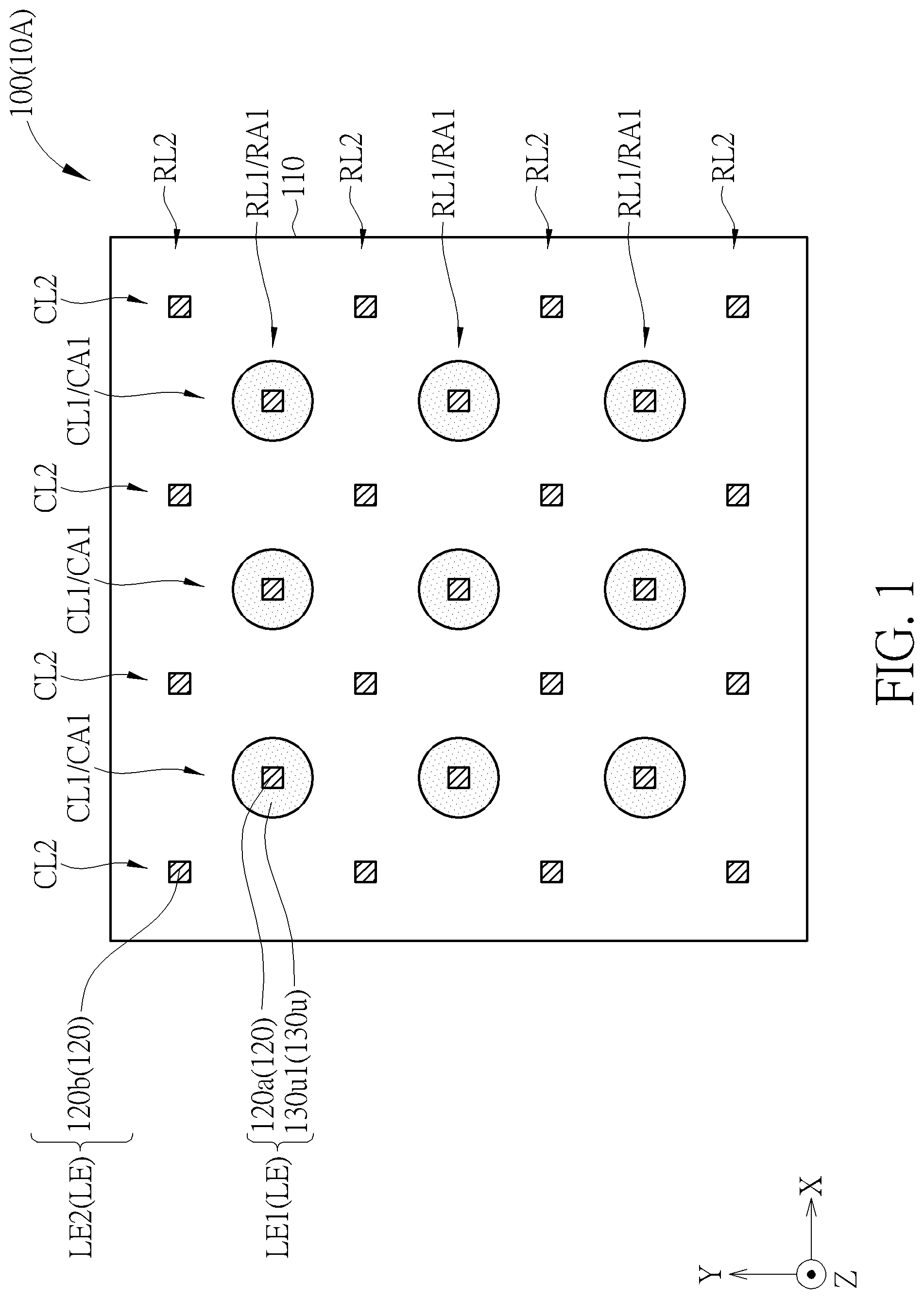
Referring to to , is a schematic diagram showing a top view of an electronic device 10 A according to a first embodiment of the present disclosure, is a schematic diagram showing cross-sectional views of exemplary designs of light emitting components according to the present disclosure, is a schematic diagram showing a cross-sectional view of a light emitting device in a first lighting mode and a second lighting mode according to a first embodiment of the present disclosure, and is a schematic diagram showing view angles of a light emitting device in a first lighting mode and a second lighting mode according to a first embodiment of the present disclosure. As shown in , the electronic device 10 A includes a light emitting device 100 , the light emitting device 100 may include a substrate 110 and a plurality of light emitting components LE disposed on the substrate 110 . The substrate 110 may be a rigid substrate or a flexible substrate. Based on the type of the substrate 110 , the substrate 110 may correspondingly include glass, quartz, ceramic, sapphire, polymer (e.g., polyimide (PI), polyethylene terephthalate (PET)), other suitable materials or a combination thereof.
As shown in , the light emitting device 100 may include a plurality of light emitting components LE disposed on the substrate 110 . In , each light emitting component LE may include a light emitting unit 120 disposed on the substrate 110 and configured to emit the light, wherein the light emitting unit 120 may be any suitable light emitting unit. For example, the light emitting unit 120 may be a light emitting diode, but not limited thereto. In some embodiments, the light emitting unit 120 of the light emitting component LE may emit the light in multiple directions to serve as a scattered light source, but not limited thereto. Moreover, in the present disclosure, the color of the light emitted from the light emitting unit 120 may be designed based on requirement(s). In some embodiments (as shown in ), the light emitting units 120 may emit the lights with the same color (e.g., the white light, the blue light or the light with other suitable color).
According to some embodiments, the light emitting components LE may include the light emitting components emitting the lights with different colors. In detail, in an embodiment, the light emitting components LE may include the light emitting units 120 emitting the lights with different colors (e.g., red light emitting units, green light emitting units, blue light emitting units). In detail, in another embodiment, the light emitting units 120 of the light emitting components LE may emit the lights with the same light, and the color conversion may be performed on the light emitting units 120 by a color conversion layer, such that the light emitting components LE may include the light emitting components emitting the lights with different colors (e.g., red light emitting components, green light emitting components and blue light emitting components). According to some embodiments, the light emitting device may be a display device, the red light emitting component, the green light emitting component and the blue light emitting component may constitute a pixel. According to some embodiments, the light emitting unit may be an OLED, a mini LED, a micro LED, or a combination thereof.
As shown in , the light emitting components LE of the light emitting device 100 may include a plurality of first light emitting components LE 1 and a plurality of second light emitting components LE 2 . In detail, the first light emitting component LE 1 and the second light emitting component LE 2 are disposed on the substrate 110 . The light emitting unit 120 included in the first light emitting component LE 1 is referred as a first light emitting unit 120 a, and the light emitting unit 120 included in the second light emitting component LE 2 is referred as a second light emitting unit 120 b. According to some embodiments, although the first light emitting unit 120 a and the second light emitting unit 120 b have different names, the structure and the lighting effect of the first light emitting unit 120 a may be the same as the structure and the lighting effect of the second light emitting unit 120 b. According to some embodiments, the first light emitting unit 120 a and the second light emitting unit 120 b may be the same. According to some embodiments, the first light emitting unit 120 a and the second light emitting unit 120 b may be different.
As shown in and , in the present disclosure, the first light emitting component LE 1 and the second light emitting component LE 2 may be distinguished by the light types of their emitting lights. The light emitting device 100 emits the light towards the direction Z (the light-emitting direction). The first light emitting component LE 1 includes a first light emitting unit 120 a and a first light controlling unit 130 u 1 disposed on the first light emitting unit 120 a in the direction Z (the light-emitting direction). The first light emitting component LE 1 may provide a first light LL 1 with a first light type TL 1 . The second light emitting component LE 2 includes a second light emitting unit 120 b. The second light emitting component LE 2 may provide a second light LL 2 with a second light type TL 2 . The first light type TL 1 is different from the second light type TL 2 .
As shown in and , in some embodiments, the first light LL 1 of the first light emitting component LE 1 has a first view angle VA 1 , and the first light LL 1 causes the light emitting device 100 to have the first view angle VA 1 . The second light LL 2 of the second light emitting component LE 2 has a second view angle VA 2 , and the second light LL 2 causes the light emitting device 100 to have the second view angle VA 2 . The first view angle VA 1 may be less than the second view angle VA 2 , but not limited thereto. Namely, compared with the second light LL 2 of the second light emitting component LE 2 , a collimating degree of the first light LL 1 of the first light emitting component LE 1 is higher, but not limited thereto. Note that the view angle is the angle range in which the user can clearly see the light of the light emitting device 100 (e.g., see the display image), and thus, when the first view angle VA 1 is less than the second view angle VA 2 , a viewing range caused by the first view angle VA 1 is smaller than a viewing range caused by the second view angle VA 2 . In the comparison of the collimating degree, when the collimating degree of the light is higher, a ratio of a sum of the light intensity of the light within a certain angle (for example, 10°) respecting to the direction Z to a total light intensity of the light is higher, wherein the measurement of the light intensity may be measured by a suitable brightness measuring instrument (e.g., a spectroradiometer, a conometer or other suitable instrument).
In the present disclosure, any suitable method may be used to make the first light LL 1 generated by the first light emitting component LE 1 have the first light type TL 1 , any suitable method may be used to make the second light LL 2 generated by the second light emitting component LE 2 have the second light type TL 2 . In some embodiments, the exemplary designs of the light emitting components LE shown in may be applied to the first light emitting component LE 1 and/or the second light emitting component LE 2 shown in . In the exemplary design DSN 1 shown in , the light emitting component LE includes a light emitting unit 120 , but the light emitting component LE does not include another structure for adjusting the light path. Therefore, the light L 0 generated by the light emitting unit 120 is the light L 1 generated by the light emitting component LE. In the exemplary design DSN 2 and the exemplary design DSN 3 shown in , the light emitting component LE may include a light emitting unit 120 and a light controlling unit 130 u disposed on the light emitting unit 120 in the direction Z (i.e., the light-emitting direction), so as to adjust the light L 0 emitted from the light emitting unit 120 to form the light L 2 or the light L 3 with another light type. In some embodiments, the light controlling unit 130 u of the exemplary design DSN 2 and the light controlling unit 130 u of the exemplary design DSN 3 may be an optical film, and the light controlling unit 130 u may include any suitable material. For example, the light controlling unit 130 u may include glass, polymer (e.g., resin), crystal, other suitable material or a combination thereof, so as to make the light controlling unit 130 u be a passive light controlling unit, but not limited thereto. In some embodiments, in , the light controlling unit 130 u of the exemplary design DSN 2 and the light controlling unit 130 u of the exemplary design DSN 3 may include a liquid crystal lens including the liquid crystal, such that the light controlling unit 130 u may control the light through electric signal(s) and serve as an electrically controlled light-controlling unit (or referred as an active light controlling unit).
For example, the light controlling unit 130 u of the exemplary design DSN 2 shown in may include a lens (e.g., a convex lens or a Fresnel lens), the light controlling unit 130 u of the exemplary design DSN 3 shown in may include a prism (e.g., a triangular prism), but not limited thereto. For example, if the light controlling unit 130 u of the exemplary design DSN 2 shown in includes liquid crystal molecules, the light controlling unit 130 u of the exemplary design DSN 2 may include a liquid crystal lens, but not limited thereto. In , since the exemplary design DSN 2 and the exemplary design DSN 3 additionally have the light controlling unit 130 u configured to control the light generated by the light emitting unit 120 compared with the exemplary design DSN 1 , the light L 2 generated by the light emitting unit 120 of the exemplary design DSN 2 and the light L 3 generated by the light emitting unit 120 of the exemplary design DSN 3 have the light type with higher collimating degree compared with the scattering light L 1 generated by the light emitting component LE of the exemplary design DSN 1 .
In the embodiment shown in , the light controlling unit 130 u may include the first light controlling unit 130 u 1 belonging to the first light emitting component LE 1 (i.e., the first light emitting component LE 1 includes the first light controlling unit 130 u 1 ), the first light controlling unit 130 u 1 is disposed on the first light emitting unit 120 a in the direction Z (i.e., the light-emitting direction), and the first light emitting unit 120 a between the substrate 110 and the first light controlling unit 130 u 1 ), so as to adjust the light emitted from the first light emitting unit 120 a. Therefore, the first light emitting component LE 1 generates the first light LL 1 with the first light type TL 1 . For example, the exemplary design DSN 2 shown in may be applied to the first light emitting component LE 1 shown in . Namely, the first light controlling unit 130 u 1 may include a lens, such that the first light emitting component LE 1 generates the first light LL 1 with the first light type TL 1 (as shown in ), but not limited thereto. The exemplary design DSN 1 shown in may be applied to the second light emitting component LE 2 shown in , such that the second light emitting component LE 2 generates the second light LL 2 with the second light type TL 2 (as shown in ), but not limited thereto.
In the embodiment shown in , the second light emitting component LE 2 may not include the light controlling unit 130 u. Namely, the first light controlling unit 130 u 1 is not disposed on the second light emitting unit 120 b. The first light controlling unit 130 u 1 is not disposed on the second light emitting unit 120 b in the direction Z, such that the light emitted from the second light emitting unit 120 b is the second light LL 2 with the second light type TL 2 of the second light emitting component LE 2 . For example, the exemplary design DSN 1 shown in may be applied to the second light emitting component LE 2 shown in , such that the second light emitting component LE 2 generates the second light LL 2 with the second light type TL 2 (as shown in ), but not limited thereto. For example, the first light LL 1 with the first light type TL 1 generated by the first light emitting component LE 1 may be a collimating light, and the second light LL 2 with the second light type TL 2 generated by the second light emitting component LE 2 may be a scattering light, but not limited thereto.
According to some embodiments, as shown in , in the condition that the first light emitting component LE 1 includes the first light controlling unit 130 u 1 disposed on the first light emitting unit 120 a in the direction Z (i.e., the light-emitting direction), although the light controlling unit is not disposed on the second light emitting unit 120 b in the light-emitting direction (the direction Z) in the second light emitting component LE 2 , other light controlling unit (not shown in ) may be optionally disposed on a side of the second light emitting unit 120 b in the side direction (the direction X or the direction Y). The material included in other light controlling unit may include such as a light absorbing material, a light reflecting material, or combination thereof. Other light controlling unit and the first light controlling unit 130 u 1 may have different shapes and/or different materials.
In the present disclosure, the corresponding relation between the first light emitting unit 120 a and the first light controlling unit 130 u 1 may be designed based on requirement(s), so as to make the first light LL 1 generated by the first light emitting component LE 1 have suitable first light type TL 1 . For example, in the first light emitting component LE 1 shown in and , the first light emitting units 120 a and the first light controlling units 130 u 1 are arranged to make them have a one-to-one relation in the direction Z, but not limited thereto. For example, in and , one first light emitting component LE 1 may include one first light controlling unit 130 u 1 , but not limited thereto. For example, in the first light emitting component LE 1 shown in , the first light emitting unit 120 a may be disposed at the center of the first light controlling unit 130 u 1 in the direction X and the direction Y, such that the first light controlling unit 130 u 1 may uniformly collimate the light generated by the first light emitting unit 120 a and control the view angle of the light emitting device 100 in the direction X and the direction Y, but not limited thereto.
As shown in and , in the operation of the light emitting device 100 , the light emitting device 100 may have a first lighting mode S 1 (or referred as a narrow view mode or a privacy mode) and a second lighting mode S 2 (or referred as a wide view mode or a sharing mode), and the light emitting device 100 may be switchable between the first lighting mode S 1 and the second lighting mode S 2 , wherein a viewable angle (i.e., the first view angle VA 1 ) of the light emitting device 100 in the first lighting mode S 1 may be less than a viewable angle (i.e., the second view angle VA 2 ) of the light emitting device 100 in the second lighting mode S 2 .
As shown in and , in some embodiments, in the first lighting mode S 1 , the first light emitting unit 120 a of the first light emitting component LE 1 may be turned on to make the first light emitting component LE 1 provide the first light LL 1 with the first light type TL 1 , and the second light emitting unit 120 b of the second light emitting component LE 2 may be turned off. In the second lighting mode S 2 , the second light emitting unit 120 b of the second light emitting component LE 2 may be turned on to make the second light emitting component LE 2 provide the second light LL 2 with the second light type TL 2 , and the first light emitting unit 120 a of the first light emitting component LE 1 may be turned off, but not limited thereto. In some embodiments (not shown in figures), in the first lighting mode S 1 , the first light emitting unit 120 a of the first light emitting component LE 1 may be turned on, the second light emitting unit 120 b of the second light emitting component LE 2 may be turned off; in the second lighting mode S 2 , both of the first light emitting unit 120 a of the first light emitting component LE 1 and the second light emitting unit 120 b of the second light emitting component LE 2 may be turned on, but not limited thereto.
According to some embodiments, in the first lighting mode S 1 , all of the first light emitting units 120 a disposed on the substrate 110 are turned on, and all of the second light emitting units 120 b disposed on the substrate 110 are turned off. According to some embodiments, in the second lighting mode S 2 , all of the second light emitting units 120 b disposed on the substrate 110 are turned on, and all of the first light emitting units 120 a disposed on the substrate 110 are turned off.
According to some embodiments, in the first lighting mode S 1 , a first portion of the first light emitting units 120 a disposed on the substrate 110 may be turned on, and a portion of the second light emitting units 120 b disposed on the substrate 110 may be turned off (but a second portion of the second light emitting units 120 b may be turned on). A number of the light emitting units in the first portion may be greater than a number of the light emitting units in the second portion. According to some embodiments, in the second lighting mode S 2 , a third portion of the second light emitting units 120 b disposed on the substrate 110 may be turned on, and a portion of the first light emitting units 120 a disposed on the substrate 110 may be turned off (but a fourth portion of the first light emitting units 120 a may be turned on). A number of the light emitting units in the third portion may be greater than a number of the light emitting units in the fourth portion.
In some embodiments, the light emitting device 100 may be switched between the lighting modes through a driving circuit (not shown in figures) electrically connected to the light emitting unit 120 of the light emitting component LE, and the driving circuit may be disposed at any suitable position in the light emitting device 100 . For example, the driving circuit may be disposed a peripheral region outside the light-emitting region of the light emitting device 100 , but not limited thereto. In some embodiments, the light emitting device 100 may further include a conductive trace electrically connected between the light emitting unit 120 and the driving circuit, and the conductive trace may be disposed on the substrate 110 or disposed in the substrate 110 . The driving circuit may include a data circuit (data IC), a gate circuit (gate IC), a printed circuit board (PCB), a flexible printed circuit board (FPC), a central processing unit (CPU) or a combination thereof, but not limited thereto.
In the present disclosure, the number and arrangement of the first light emitting components LE 1 and the number and arrangement of the second light emitting components LE 2 may be designed suitably, such that the light emitting device 100 has a uniform light emitting function in the first lighting mode S 1 and the second lighting mode S 2 both. In some embodiments, the number of the first light emitting components LE 1 may be the same as the number of the second light emitting components LE 2 , such that the light intensity of the light emitting device 100 in the first lighting mode S 1 may be the same as or similar to the light intensity of the light emitting device 100 in the second lighting mode S 2 , but not limited thereto.
In some embodiments, the first light emitting components LE 1 and the second light emitting components LE 2 may be evenly distributed in the light emitting device 100 , so as to make the light emitting device 100 have the uniform light emitting function in the first lighting mode S 1 and the second lighting mode S 2 . As shown in , the first light emitting components LE 1 may be arranged into a plurality of first light emitting columns CL 1 and a plurality of first light emitting rows RL 1 , and the second light emitting components LE 2 may be arranged into a plurality of second light emitting columns CL 2 and a plurality of second light emitting rows RL 2 . In detail, the first light emitting column CL 1 include a plurality of first light emitting components LE 1 arranged in the direction Y (the first direction). The second light emitting column CL 2 includes a plurality of second light emitting components LE 2 arranged in the direction Y (the first direction). The first light emitting components LE 1 of the first light emitting column CL 1 and the second light emitting components LE 2 of the second light emitting column CL 2 are staggered in the direction X (the second direction). The direction Y (the first direction) and the direction X (the second direction) are not parallel to each other (e.g., the direction Y and the direction Y are perpendicular to each other).
As shown in , the first light emitting components LE 1 included in the first light emitting row RL 1 may be arranged in the direction X (the second direction), the second light emitting components LE 2 included in the second light emitting row RL 2 may be arranged in the direction X (the second direction), the first light emitting column CL 1 and the second light emitting column CL 2 may be arranged alongside in the direction X (the second direction), the first light emitting row RL 1 and the second light emitting row RL 2 may be arranged alongside in the direction Y (the first direction), and the second direction may not be parallel to the first direction, but not limited thereto. For example (as shown in ), the first light emitting columns CL 1 and the second light emitting columns CL 2 are arranged alternately in the direction X (the second direction), and the first light emitting rows RL 1 and the second light emitting rows RL 2 are arranged alternately in the direction Y (the first direction), but not limited thereto. For instance (as shown in ), the first light emitting components LE 1 in the first light emitting column CL 1 and the second light emitting components LE 2 in the second light emitting column CL 2 are staggered in the direction X (the second direction), and the first light emitting components LE 1 in the first light emitting row RL 1 and the second light emitting components LE 2 in the second light emitting row RL 2 are staggered in the direction Y (the first direction), but not limited thereto. For instance (as shown in ), the first light emitting components LE 1 may be arranged in an array in the direction X (the second direction) and the direction Y (the first direction), and the second light emitting components LE 2 may be arranged in an array in the direction X (the second direction) in the direction Y (the first direction), but not limited thereto.
As shown in , the first light controlling units 130 u 1 of the first light emitting components LE 1 may be arranged into a plurality of first light controlling rows RA 1 and a plurality of first light controlling columns CA 1 , wherein the first light controlling units 130 u 1 included in the first light controlling column CA 1 may be arranged in the direction Y (the first direction), and the first light controlling units 130 u 1 included in the first light controlling row RA 1 may be arranged in the direction X (the second direction), but not limited thereto. For example (as shown in ), the first light controlling units 130 u 1 may be arranged in an array in the direction Y (the first direction) and the direction X (the second direction), but not limited thereto.
shows the electronic device 10 A. The electronic device 10 A includes a backlight module BLM and a display panel DP. The backlight module BLM may be a light source providing light for the display panel DP. The backlight module BLM may be designed based on the aforementioned light emitting device 100 , and this part will not be redundantly described. According to the above, based on the mode of the backlight module BLM, the backlight module BLM (i.e., the light emitting device 100 ) may provide the backlight with narrow view angle (e.g., the first lighting mode S 1 ) or the backlight with wide view angle (e.g., the second lighting mode S 2 ). Accordingly, the electronic device 10 A using this backlight module BLM (i.e., the light emitting device 100 ) may have the privacy mode (the first lighting mode S 1 ) with narrower view angle and the sharing mode (the second lighting mode S 2 ) with wider view angle. As shown in , the display panel DP may be a liquid crystal display panel, but not limited thereto.
In , the electronic device 10 A may include a light diffuser DF disposed between the display panel DP and the backlight module BLM, so as to uniform the backlight generated by the backlight module BLM (i.e., the light generated by the first light emitting component LE 1 and the second light emitting component LE 2 ), and to reduce the poor display phenomenon that may be caused by insufficient density of the light emitting components LE in the backlight module BLM. In , in order to enhance the backlight uniformity, an air gap may exist between the light diffuser DF and the backlight module BLM, and the size (distance) of the air gap AG in the direction Z may be designed based on requirement(s). For example, the distance of the air gap AG in the direction Z may range from 0.1 mm to 10 mm or range from 2 mm to 7 mm, but not limited thereto.
According to the above, in a traditional electronic device with a privacy function, a privacy cell including a privacy medium layer needs to be additional disposed in the traditional electronic device. However, due to the existence of the privacy cell, the light transmittance of the traditional electronic device is decreased. On the contrary, in the electronic device of the present disclosure, through the design of the light emitting component, the light emitting component provides the lights with different light types, such that the electronic device has the privacy mode and the sharing mode. Thus, the privacy cell having the privacy medium layer does not exist in the electronic device of the present disclosure. Compared with the traditional electronic device, the design of the electronic device of the present disclosure may enhance the light transmittance of the electronic device and make the electronic device have the excellent display function.
The light emitting device of the present disclosure is not limited to the above embodiments. Further embodiments of the present disclosure are described below. For ease of comparison, same components will be labeled with the same symbol in the following. The following descriptions relate the differences between each of the embodiments, and repeated parts will not be redundantly described.
Referring to , is a schematic diagram showing a top view of an electronic device 20 A according to a second embodiment of the present disclosure. The electronic device 20 A includes a light emitting device 200 . As shown in , a main difference between this embodiment and the first embodiment is the design of the first light controlling unit 130 u 1 . In the light emitting device 200 shown in , the first light emitting component LE 1 includes a plurality of first light emitting units 120 a and one first light controlling unit 130 u 1 . The first light controlling unit 130 u 1 is disposed on the plurality of first light emitting units 120 a in the direction Z (the light-emitting direction). In , one first light controlling unit 130 u 1 is disposed on three first light emitting units 120 a, and the first light controlling unit 130 u 1 extends along the direction Y (the first direction). That is to say, three first light emitting units 120 a is corresponding to one first light controlling unit 130 u 1 . In the top view, the first light controlling unit 130 u 1 may be a strip structure extending along the direction Y. The first light controlling unit 130 u 1 may cover the first light emitting units 120 a. For convenience, only shows that three first light emitting units 120 a is corresponding to one first light controlling unit 130 u 1 . In other embodiment, the number of the first light emitting units 120 a corresponding to one first light controlling unit 130 u 1 is not limited to three.
According to the design of the first light controlling unit 130 u 1 shown in , in the light emitted from the first light emitting unit 120 a, the first light controlling unit 130 u 1 may adjust a direction of a light component parallel to the direction X in this light to make it approach the direction Z, and the first light controlling unit 130 u 1 may not adjust a direction of a light component parallel to the direction Y in this light. Accordingly, the first light controlling unit 130 u 1 may collimate the light component parallel to the direction X in the light, so as to control the view angle in the direction X.
In the present disclosure, the arrangements of the first light emitting components LE 1 and the second light emitting components LE 2 may be designed based on requirement(s), and the arrangements the first light emitting units 120 a and the second light emitting units 120 b may be designed based on requirement(s). For instance (as shown in ), the first light emitting units 120 a and the second light emitting units 120 b may be arranged in an array in the direction X and the direction Y, but not limited thereto. According to some embodiments, the first light emitting units 120 a and the second light emitting units 120 b may be arranged alternately in the direction X, but not limited thereto. According to some embodiments, as shown in , the first light emitting unit 120 a may be aligned with the second light emitting unit 120 b in the direction X, but not limited thereto.
Referring to and , is a schematic diagram showing a top view of an electronic device 30 A according to a third embodiment of the present disclosure, wherein the electronic device 30 A includes a light emitting device 300 . is a schematic diagram showing cross-sectional views of exemplary designs of light emitting components according to the present disclosure. As shown in and , a main difference between this embodiment and the first embodiment is the design of the light controlling unit 130 u. In some embodiments, the exemplary designs of the light emitting components LE shown in and the exemplary design DSN 1 of the light emitting component LE shown in may be applied to the first light emitting component LE 1 and/or the second light emitting component LE 2 shown in . The detail of the exemplary design DSN 1 shown in may be referred to the above, and this part will not be redundantly described. In an exemplary design DSN 4 , an exemplary design DSN 5 , an exemplary design DSN 6 , an exemplary design DSN 7 and an exemplary design DSN 8 shown in , the light emitting component LE may include the light emitting unit 120 and the light controlling unit 130 u. The light controlling unit 130 u may be disposed on at least one side of the light emitting unit 120 in the horizontal direction (i.e., a side direction of the light emitting unit 120 ), so as to adjust the light emitted from the light emitting unit 120 to form a light L 4 , a light L 5 , a light L 6 , a light L 7 or a light L 8 with another light type.
In the exemplary design DSN 4 , the exemplary design DSN 5 and the exemplary design DSN 6 shown in , the light controlling unit 130 u may include a blocking wall configured to absorb the light emitted from the light emitting unit 120 and having an angle greater than a specific value and respecting to the direction Z. In some embodiments, the blocking wall may include a light absorbing material. For example, the light absorbing material of the blocking wall of the light controlling unit 130 u may include black photoresist, black ink, black resin, black pigment, other suitable light absorbing material or a combination thereof, so as to make the light controlling unit 130 u be a passive light controlling unit, but not limited thereto. In some embodiments, the material of the blocking wall of the light controlling unit 130 u may include a polymer dispersed liquid crystal (PDLC) unit, a polymer network liquid crystal (PNLC) unit, other suitable material or a combination thereof, such that light controlling unit 130 u may control the light through electric signal(s) and serve as an electrically controlled light-controlling unit (or referred as an active light controlling unit).
As shown in , the exemplary designs DSN 4 , DSN 5 and DSN 6 may be applied to the first light emitting component LE 1 and the second light emitting component LE 2 of the present disclosure. A first height H 1 of the light controlling unit 130 u in the exemplary design DSN 5 is greater than a second height H 2 of the light controlling unit 130 u in the exemplary design DSN 4 , such that the collimating degree of the light L 5 generated by the light emitting component LE in the exemplary design DSN 5 is greater than the collimating degree of the light L 4 generated by the light emitting component LE in the exemplary design DSN 4 . A distance D 22 between the light controlling unit 130 u and the light emitting unit 120 in the exemplary design DSN 6 is greater than a distance D 11 between the light controlling unit 130 u and the light emitting unit 120 in the exemplary design DSN 5 , such that the collimating degree of the light L 5 generated by the exemplary design DSN 5 is greater than the collimating degree of the light L 6 of the exemplary design DSN 6 . In the present disclosure, the distance between the light controlling unit 130 u and the light emitting unit 120 is their minimum distance.
According to the exemplary designs DSN 7 and DSN 8 shown in , the light controlling unit 130 u may include a reflective structure configured to reflect the light generated by the light emitting unit 120 . In some embodiments, the light controlling unit 130 u of the exemplary design DSN 7 and the light controlling unit 130 u of the exemplary design DSN 8 may include a reflective material (e.g., metal), such that the light controlling unit 130 u has a reflective surface to be a reflective structure. For example, the light controlling unit 130 u of the exemplary design DSN 7 and the light controlling unit 130 u of the exemplary design DSN 8 may include a curved reflective structure (e.g., a curved surface reflector), but not limited thereto. For example, the curved surface of the curved reflective structure may be a spherical surface, a parabolic surface or other suitable curved surface. For example, in the exemplary design DSN 7 , an inner surface 1371 of the light controlling unit 130 u includes a curved surface for reflecting light, and an outer surface 1372 of the light controlling unit 130 u includes a curved surface. In the exemplary design DSN 8 , an inner surface 1381 of the light controlling unit 130 u includes a curved surface for reflecting light, and an outer surface 1382 of the light controlling unit 130 u includes a plane (e.g., a plane perpendicular to the substrate 110 ), but not limited thereto. Accordingly, in the exemplary designs DSN 7 and DSN 8 , the light controlling units 130 u may reflect the light generated by the light emitting units 120 and having an angle greater than a specific value and respecting to the direction Z, such that the light emitting components LE generate the collimated light L 7 and the collimated light L 8 respectively. In the present disclosure, the exemplary designs DSN 7 and DSN 8 may be applied to the first light emitting component LE 1 or the second light emitting component LE 2 of any embodiment of the present disclosure. According to some embodiments, the exemplary designs DSN 7 and DSN 8 may be applied to the second light emitting component LE 2 of any embodiment of the present disclosure, so as to provide the second light LL 2 having the wider view angle (e.g., the second view angle VA 2 ), as shown in .
According to some embodiments, in the exemplary design DSN 4 , the exemplary design DSN 5 and the exemplary design DSN 6 shown in , the material of the light controlling unit 130 u does not exist at a surface in contact with the bottom of the light emitting unit 120 . Namely, the material of the surface in contact with the bottom of the light emitting unit 120 is different from the material of the light controlling unit 130 u. According to some embodiments, in the exemplary design DSN 7 and the exemplary design DSN 8 shown in , the light emitting unit 120 may be disposed on a portion of the light controlling unit 130 u (e.g., a bottom 1374 and a bottom 1384 ), and another portion of the light controlling unit 130 u (e.g., a sidewall 1376 and a sidewall 1386 ) may be disposed on at least one side of the light emitting unit 120 in the horizontal direction (i.e., the side direction of the light emitting unit 120 ).
As shown in , the light emitting device 300 includes a plurality of light controlling units 130 u disposed on the substrate 110 . The first light emitting component LE 1 is disposed on the substrate 110 , the first light emitting component LE 1 includes the first light emitting unit 120 a and the first light controlling unit 130 u 1 , and the first light controlling unit 130 u 1 is disposed on a side of the first light emitting unit 120 a in the side direction (the horizontal direction, the direction on the XY surface) to adjust the light emitted from the first light emitting unit 120 a, such that the first light emitting component LE 1 generates the first light LL 1 with the first light type TL 1 . For example, the exemplary design DSN 4 , the exemplary design DSN 5 or the exemplary design DSN 6 shown in may be applied to the first light emitting component LE 1 shown in , but not limited thereto. The plurality of light controlling units 130 u includes the first light controlling unit 130 u 1 . The second light emitting component LE 2 is disposed on the substrate 110 , and the second light emitting component includes the second light emitting unit 120 b. The first light emitting component LE 1 may provide the first light LL 1 with the first light type TL 1 , such as the exemplary design DSN 5 shown in . The second light emitting component LE 2 may provide the second light LL 2 with the second light type TL 2 , such as the exemplary design DSN 1 shown in . The first light type TL 1 is different from the second light type TL 2 . As shown in , the first light controlling unit 130 u 1 may include the light absorbing material. The light absorbing material may be the blocking wall configured to absorb the light emitted from the light emitting unit 120 and having an angle greater than a specific value and respecting to the direction Z. The light absorbing material may include black photoresist, black ink, black resin, black pigment, other suitable light absorbing material or a combination thereof.
As shown in , one of the light controlling units 130 u closest to the second light emitting unit 120 b is a reference light controlling unit 130 f. The first light emitting component LE 1 or the second light emitting component LE 2 includes the reference light controlling unit 130 f. As an example, shows a second light emitting unit 120 bb and a reference light controlling unit 130 f closest to the second light emitting unit 120 bb. In this embodiment, the reference light controlling unit 130 f is the first light controlling unit 130 u 1 . A first distance D 1 between the first light emitting unit 120 a and the first light controlling unit 130 u 1 is different from a second distance D 2 between the second light emitting unit 120 bb and the reference light controlling unit 130 f (the closest first light controlling unit 130 u 1 ). For instance, as shown in , the first distance D 1 may be less than the second distance D 2 , but not limited thereto. For example, in , the first distance D 1 may be measured along the direction X (or the direction Y), the second distance D 2 may be measured along a direction M, wherein the direction M is a horizontal direction (perpendicular to the direction Z) not parallel to the direction X and the direction Y, but not limited thereto. Note that an angle α between the direction M and the direction X may be greater than 0 degrees and less than 90 degrees (i.e., an acute angle) or be greater than 90 degrees and less than 180 degrees (i.e., an obtuse angle). For example, the angle α shown in is an acute angle. Note that the measuring directions of the first distance D 1 and the second distance D 2 may be changed according to the design of the light controlling unit(s) 130 u and the arrangement of the light emitting components LE.
For example, in , the first light controlling unit 130 u 1 may surround the first light emitting unit 120 a to absorb the light emitted from the first light emitting unit 120 a and having an angle greater than a specific value and respecting to the direction Z, so as to control the view angle in the direction X and the direction Y, but not limited thereto. In the embodiment shown in , the second light emitting component LE 2 may not include the light controlling unit 130 u, such that the second light LL 2 with the second light type TL 2 generated by the second light emitting component LE 2 is the light emitted from the second light emitting unit 120 b. For example, the exemplary design DSN 1 shown in may be applied to the second light emitting component LE 2 shown in , such that the second light emitting component LE 2 generates the second light LL 2 with the second light type TL 2 , but not limited thereto. The collimating degree of the first light LL 1 generated by the first light emitting component LE 1 is greater than the collimating degree of the second light LL 2 generated by the second light emitting component LE 2 , but not limited thereto.
Referring to , is a schematic diagram showing a top view of an electronic device 40 A according to a fourth embodiment of the present disclosure. The electronic device 40 A includes a light emitting device 400 . As shown in , a main difference between this embodiment and the third embodiment is the design of the first light controlling unit 130 u 1 . In the light emitting device 400 shown in , the first light emitting component LE 1 includes a plurality of first light emitting units 120 a and one first light controlling unit 130 u 1 , and the first light controlling unit 130 u 1 is disposed on a side of the first light emitting units 120 a in the side direction (i.e., the horizontal direction, the direction on the XY surface). In , one first light controlling unit 130 u 1 is disposed on a side of three first light emitting units 120 a in the side direction (i.e., the horizontal direction, the direction on the XY surface) and extends along the direction Y (the first direction). Namely, three first light emitting units 120 a is corresponding to one first light controlling unit 130 u 1 . As shown in , one first light controlling unit 130 u 1 may include two strip structures (the strip blocking walls) extending along the direction Y, and these strip structures are arranged alongside in the direction X, but not limited thereto. According to the design of the first light controlling unit 130 u 1 shown in , the first light controlling unit 130 u 1 may absorb and adjust the light generated by the first light emitting unit 120 a in the direction X, so as to achieve the collimating effect and control the view angle in the direction X.
In the present disclosure, the arrangements of the first light emitting components LE 1 and the second light emitting components LE 2 may be designed based on requirement(s), and the arrangements of the first light emitting units 120 a and the second light emitting units 120 b may be designed based on requirement(s). For example (as shown in ), the first light emitting units 120 a and the second light emitting units 120 b may be arranged in an array in the direction X and the direction Y, but not limited thereto. For example (as shown in ), the first light emitting units 120 a and the second light emitting units 120 b may be arranged alternately in the direction X, but not limited thereto. For example (as shown in ), the first light emitting unit 120 a may be aligned with the second light emitting unit 120 b in the direction X, but not limited thereto. In , the first distance D 1 and the second distance D 2 may be measured along the direction X, but not limited thereto.
Referring to , is a schematic diagram showing a top view of an electronic device 50 A according to a fifth embodiment of the present disclosure. The electronic device 50 A includes a light emitting device 500 . As shown in , a main difference between this embodiment and the first embodiment is that the light controlling units 130 u of the light emitting device 500 of the present disclosure may be divided into a plurality of first light controlling units 130 u 1 and a plurality of second light controlling units 130 u 2 . The first light controlling unit 130 u 1 may be included in the first light emitting component LE 1 and adjust the light emitted from the first light emitting unit 120 a, such that the first light emitting component LE 1 generates the first light LL 1 with the first light type TL 1 . The second light controlling unit 130 u 2 may be included in the second light emitting component LE 2 and adjust the light emitted from the second light emitting unit 120 b, such that the second light emitting component LE 2 generates the second light LL 2 with the second light type TL 2 . The aforementioned exemplary designs (as shown in and ) or the aforementioned embodiments (as shown in , , and ) may be applied to the first light controlling unit 130 u 1 and/or the second light controlling unit 130 u 2 based on requirement(s).
As shown in , in some embodiments, the first light controlling unit 130 u 1 of the first light emitting component LE 1 may be disposed on the first light emitting unit 120 a in the direction Z (i.e., the light-emitting direction), and the second light emitting component LE 2 may further include the second light controlling unit 130 u 2 disposed on the second light emitting unit 120 b in the direction Z (i.e., the light-emitting direction). In , the first light controlling unit 130 u 1 may be different from the second light controlling unit 130 u 2 , such that the first light type TL 1 of the first light LL 1 generated by the first light emitting component LE 1 may be different from the second light type TL 2 of the second light LL 2 generated by the second light emitting component LE 2 . In some embodiments (as shown in ), the first light controlling unit 130 u 1 and the second light controlling unit 130 u 2 may be different optical films. For example, the first light controlling unit 130 u 1 includes a lens of the exemplary design DSN 2 shown in , and the second light controlling unit 130 u 2 includes a prism of the exemplary design DSN 3 shown in , but not limited thereto. For example, the first light controlling unit 130 u 1 and the second light controlling unit 130 u 2 may include different lenses, but not limited thereto. For example, the first light controlling unit 130 u 1 and the second light controlling unit 130 u 2 may respective include liquid crystal lenses, and the liquid crystal lens of the first light controlling unit 130 u 1 and liquid crystal lens of the second light controlling unit 130 u 2 may be driven by different electric signals, but not limited thereto. In some embodiments (as shown in ), the collimating degree of the first light LL 1 generated by the first light emitting component LE 1 may be greater than the collimating degree of the second light LL 2 generated by the second light emitting component LE 2 , but not limited thereto.
In some embodiments (as shown in ), the first light emitting unit 120 a and the first light controlling unit 130 u 1 are arranged in a one-to-one corresponding manner in the direction Z, and the second light emitting unit 120 b and the second light controlling unit 130 u 2 are arranged in a one-to-one corresponding manner in the direction Z, but not limited thereto. For example, the first light emitting unit 120 a may be disposed at a center of the first light controlling unit 130 u 1 in the direction X and the direction Y, and the second light emitting unit 120 b may be disposed at a center of the second light controlling unit 130 u 2 in the direction X and the direction Y, but not limited thereto.
In the arrangement of the second light controlling units 130 u 2 of the second light emitting components LE 2 , the second light controlling unit 130 u 2 may be arranged into a plurality of second light controlling rows RA 2 and a plurality of second light controlling columns CA 2 , wherein the second light controlling columns CA 2 may be arranged alongside in the direction X, the second light controlling rows RA 2 may be arranged alongside in the direction Y, the second light controlling units 130 u 2 included in the second light controlling column CA 2 may be arranged in the direction Y, and the second light controlling units 130 u 2 included in the second light controlling row RA 2 may be arranged in the direction X, but not limited thereto. For instance (as shown in ), the second light controlling units 130 u 2 may be arranged in an array in the direction X and the direction Y, but not limited thereto.
Referring to , is a schematic diagram showing a top view of an electronic device 60 A according to a sixth embodiment of the present disclosure. The electronic device 60 A includes a light emitting device 600 . As shown in , a main difference between this embodiment and the fifth embodiment is the design of the first light controlling unit 130 u 1 and the design of the second light controlling unit 130 u 2 . In the light emitting device 600 shown in , the detail of the first light controlling unit 130 u 1 may be referred to the third embodiment (as shown in ) of the present disclosure, and this part will not be redundantly described. In , the second light emitting component LE 2 includes the second light controlling unit 130 u 2 , the second light controlling unit 130 u 2 is disposed on a side of the second light emitting unit 120 b in the side direction (i.e., the horizontal direction and/or the direction on the XY surface). The side direction is not parallel to the direction Z (the light-emitting direction). For instance, the second light controlling unit 130 u 2 may surround the second light emitting unit 120 b to absorb the light emitted from the second light emitting unit 120 b and having an angle greater than another specific value and respecting to the direction Z, so as to control the view angle in the direction X and the direction Y, but not limited thereto. Since the light emitting device 600 has the second light controlling unit 130 u 2 , in an example of the second light emitting unit 120 bb and the reference light controlling unit 130 f closest to the second light emitting unit 120 bb shown in , the reference light controlling unit 130 f is the second light controlling unit 130 u 2 .
In the present disclosure, the first light type TL 1 of the first light LL 1 and the second light type TL 2 of the second light LL 2 may be adjusted through the distance between the light controlling unit 130 u and the light emitting unit 120 and/or the height of the light controlling unit 130 u. As shown in and , according to some embodiments, the exemplary design DSN 5 shown in may be applied to the first light emitting component LE 1 , and the exemplary design DSN 4 shown in may be applied to the second light emitting component LE 2 . Namely, in the direction Z (the light-emitting direction), the first light controlling unit 130 u 1 of the first light emitting component LE 1 has the first height H 1 (as shown in the exemplary design DSN 5 of ), the second light controlling unit 130 u 2 of the second light emitting component LE 2 has the second height H 2 (as shown in the exemplary design DSN 4 of ), and the first height H 1 is different from the second height H 2 . According to some embodiments, the first height H 1 is greater than the second height H 2 . A ratio of the first height H 1 of the first light controlling unit 130 u 1 to the second height H 2 of the second light controlling unit 130 u 2 may range from 1.5 to 5 (e.g., range from 2 to 3), but not limited thereto.
As shown in and , according to some embodiments, the exemplary design DSN 5 shown in may be applied to the first light emitting component LE 1 shown in , and the exemplary design DSN 6 shown in may be applied to the second light emitting component LE 2 shown in . In detail, in the first light emitting component LE 1 of , the first distance D 1 exists between the first light controlling unit 130 u 1 and the first light emitting unit 120 a (or referred to the distance D 11 of the exemplary design DSN 5 shown in ). In the second light emitting component LE 2 shown in , the second distance D 2 exists between the second light controlling unit 130 u 2 (i.e., the reference light controlling unit 130 f ) and the second light emitting unit 120 b (or referred to the distance D 22 of the exemplary design DSN 6 shown in ). The first distance D 1 is different from the second distance D 2 . According to some embodiments, the first distance D 1 may be less than the second distance D 2 . In some embodiments, a ratio of the second distance D 2 to the first distance D 1 may range from 1.5 to 5 (e.g., range from 2 to 3), but not limited thereto. For instance (as shown in ), the first distance D 1 and the second distance D 2 may be measured along the direction X (or the direction Y), but not limited thereto. In some embodiments, the collimating degree of the first light LL 1 generated by the first light emitting component LE 1 may be greater than the collimating degree of the second light LL 2 generated by the second light emitting component LE 2 , but not limited thereto.
As shown in , a third distance D 3 exists between the second light emitting unit 120 b and the first light controlling unit 130 u 1 , and the first distance D 1 may be less than the third distance D 3 , but not limited thereto. As shown in , a fourth distance D 4 exists between the first light emitting unit 120 a and the second light controlling unit 130 u 2 , and the second distance D 2 may be less than the fourth distance D 4 , but not limited thereto. For instance (as shown in ), the third distance D 3 and the fourth distance D 4 may be measured along a direction M, and an angle α between the direction M and the direction X may be an obtuse angle, but not limited thereto.
Referring to , is a schematic diagram showing a top view of an electronic device 70 A according to a seventh embodiment of the present disclosure. The electronic device 70 A includes a light emitting device 700 . As shown in , a main difference between this embodiment and the fifth embodiment ( ) is the design of the second light controlling unit 130 u 2 . In the light emitting device 700 shown in , the first light controlling unit 130 u 1 of the first light emitting component LE 1 may be disposed on the first light emitting unit 120 a in the direction Z (i.e., the light-emitting direction). The second light emitting component LE 2 includes the second light controlling unit 130 u 2 disposed on a side of the second light emitting unit 120 b in the side direction (i.e., the horizontal direction and/or the direction on the XY surface), but not limited thereto. In some embodiments, the first light controlling unit 130 u 1 may include an optical film (e.g., a lens or a prism), and the second light controlling unit 130 u 2 may include a blocking wall configured to absorb light and containing a light absorbing material, but not limited thereto.
In the light emitting device of some embodiments (not shown in figures), the first light controlling unit 130 u 1 of the first light emitting component LE 1 may be disposed on a side of the first light emitting unit 120 a in the side direction (i.e., the horizontal direction and/or the direction on the XY surface), and the second light controlling unit 130 u 2 of the second light emitting component LE 2 may be disposed on the second light emitting unit 120 b in the direction Z (i.e., the light-emitting direction), but not limited thereto. In some embodiments, the first light controlling unit 130 u 1 may include a blocking wall configured to absorb light and containing a light absorbing material, and the second light controlling unit 130 u 2 may include an optical film (e.g., a lens or a prism), but not limited thereto.
Referring to , is a schematic diagram showing a top view of an electronic device 80 A according to an eighth embodiment of the present disclosure. The electronic device 80 A includes a light emitting device 800 . As shown in , a main difference between this embodiment and the first embodiment is the design of the light emitting unit 120 . The light emitting device 800 shown in may include a plurality kinds of first light emitting components LE 1 and a plurality kinds of the second light emitting components LE 2 . Different kinds of the first light emitting components LE 1 may respectively include the first light emitting units 120 a emitting the lights with different colors, and different kinds of the second light emitting components LE 2 may respectively include the second light emitting units 120 b emitting the lights with different colors. For example (as shown in ), the light emitting device 800 may include three kinds of the first light emitting components LE 1 (e.g., the first light emitting component LE 1 _ 1 , the first light emitting component LE 1 _ 2 and the first light emitting component LE 1 _ 3 ) and three kinds of the second light emitting components LE 2 (e.g., the second light emitting component LE 2 _ 1 , the second light emitting component LE 2 _ 2 and the second light emitting component LE 2 _ 3 ), wherein the first light emitting unit 120 a 1 of the first light emitting component LE 1 _ 1 and the second light emitting unit 120 b 1 of the second light emitting component LE 2 _ 1 may emit lights with a first color (e.g., red), the first light emitting unit 120 a 2 of the first light emitting component LE 1 _ 2 and the second light emitting unit 120 b 2 of the second light emitting component LE 2 _ 2 may emit lights with a second color (e.g., green), and the first light emitting unit 120 a 3 of the first light emitting component LE 1 _ 3 and the second light emitting unit 120 b 3 of the second light emitting component LE 2 _ 3 may emit lights with a third color (e.g., blue), but not limited thereto.
For example (not shown in figures), one first light emitting component LE 1 may include a plurality of first light emitting units 120 a respectively emitting the lights with different colors, and one of the first light controlling units 130 u 1 in this the first light emitting component LE 1 may be corresponding to these first light emitting units 120 a emitting the lights with different colors; one second light emitting component LE 2 may include a plurality of second light emitting units 120 b respectively emitting the lights with different colors, and if this second light emitting component LE 2 has one second light controlling unit 130 u 2 , this second light controlling unit 130 u 2 may be corresponding to these the second light emitting units 120 b emitting the lights with different colors, but not limited thereto.
In summary, in the electronic device of the present disclosure, owing to the designs of the light emitting components, the light emitting components provides the lights with different light types, such that the electronic device has the privacy mode and the sharing mode. According to some embodiments, the first light emitting component and the second light emitting component provides the lights with different light types through the light adjustment of the light controlling unit(s) in the light emitting component(s). Also, through the control of turning on/off the first light emitting component and turning on/off the second light emitting component, the light emitting device has different lighting modes to make the light emitting device have the privacy function. Compared with the traditional electronic device, the privacy cell having the privacy medium layer does not exist in the electronic device of the present disclosure, so as to enhance the light transmittance of the electronic device and make the electronic device have the excellent display function.
Although the embodiments and their advantages of the present disclosure have been described as above, it should be understood that any person having ordinary skill in the art can make changes, substitutions, and modifications without departing from the spirit and scope of the present disclosure. In addition, the protecting scope of the present disclosure is not limited to the processes, machines, manufactures, material compositions, devices, methods and steps in the specific embodiments described in the description. Any person having ordinary skill in the art can understand the current or future developed processes, machines, manufactures, material compositions, devices, methods and steps from the content of the present disclosure, and then, they can be used according to the present disclosure as long as the same functions can be implemented or the same results can be achieved in the embodiments described herein. Thus, the protecting scope of the present disclosure includes the above processes, machines, manufactures, material compositions, devices, methods and steps. Moreover, each claim constitutes an individual embodiment, and the protecting scope of the present disclosure also includes the combination of each claim and each embodiment. The protecting scope of the present disclosure shall be determined by the appended claims.
Those skilled in the art will readily observe that numerous modifications and alterations of the device and method may be made while retaining the teachings of the disclosure. Accordingly, the above disclosure should be construed as limited only by the metes and bounds of the appended claims.
Figures (13)
Citations
This patent cites (11)
- US11842701
- US2020/0096822
- US2020/0312821
- US2023/0269993
- US2024/0027672
- US2024/0264486
- US108761854
- US113777692
- US115327820
- US201930936
- US202132869