Image Sensor Including Shared Pixels
Abstract
An image sensor may include a first shared pixel region and a first isolation layer on a substrate, the first isolation layer defining the first shared pixel region. The first shared pixel region may include photo-sensing devices in sub-pixel regions and a first floating diffusion region connected to the photo-sensing devices. The sub-pixel regions may include a first sub-pixel region and a second sub-pixel region that constitute a first pixel group region. The sub-pixel regions may include a third sub-pixel region and a fourth sub-pixel region that constitute a second pixel group region. The first shared pixel region may include first and second well regions doped with first conductivity type impurities. The second well region may be spaced apart from the first well region. The first pixel group region may share a first well region. The second pixel group region may share the second well region.
Claims (11)
1. An image sensor comprising: a substrate having a first surface and a second surface; and a plurality of shared pixel regions formed in the substrate, the plurality of shared pixel regions arranged in a first direction and a second direction perpendicular to the first direction; wherein each of the plurality of shared pixel regions includes a first pixel group region and a second pixel group region arranged in the second direction, wherein each of the first pixel group region and the second pixel group region includes a first sub-pixel region and a second sub-pixel region arranged in the first direction, wherein each of the first sub-pixel region and the second sub-pixel region includes a photo sensing region on the first surface of the substrate, wherein each of the first pixel group region and the second pixel group region includes a first well region doped with first conductivity type impurities and formed on the photo sensing region in a third direction perpendicular to the first direction and the second direction, and wherein different first well regions in each of the plurality of shared pixel regions are separated from each other.
Show 10 dependent claims
2. The image sensor of claim 1 , wherein an impurity concentration of the first well region is lower than an impurity concentration of the photo sensing region.
3. The image sensor of claim 1 , further comprising: a first isolation layer extended from the second surface of the substrate, the first isolation layer defining each of the plurality of shared pixel regions; and a second isolation layer extended from the second surface of the substrate, the second isolation layer disposed between the first pixel group region and the second pixel group region.
4. The image sensor of claim 1 , further comprising: a first isolation layer extended from the second surface of the substrate, the first isolation layer defining each of the plurality of shared pixel regions; and a second isolation layer extended from the second surface of the substrate, the second isolation layer disposed between the first sub-pixel region and the second sub-pixel region.
5. The image sensor of claim 1 , wherein charges generated in each of the first sub-pixel region and the second sub-pixel region included in a same pixel group region among the first pixel group region and the second pixel group region are movable to each other.
6. The image sensor of claim 1 , further comprising: a second well region doped with second conductivity type impurities and disposed between each of the plurality of shared pixel regions.
7. The image sensor of claim 6 , further comprising: a first isolation layer extended from the second surface of the substrate, the first isolation layer defining each of the plurality of shared pixel regions; and wherein the second well region surrounds the first isolation layer in the third direction.
8. The image sensor of claim 1 , further comprising: a plurality of color filters on the second surface of the substrate, wherein a corresponding color filter among the plurality of color filters is disposed on each of the plurality of shared pixel regions.
9. The image sensor of claim 1 , further comprising: a plurality of microlens on the second surface of the substrate, wherein a corresponding microlens among the plurality of microlens is disposed on each of the plurality of shared pixel regions.
10. The image sensor of claim 9 , wherein the image sensor performs an AF function using a first pixel signal and a second pixel signal, the first pixel signal is a signal according to charges generated in the first sub-pixel region and the second sub-pixel region included in the first pixel group region, and the second pixel signal is a signal according to charges generated in the first sub-pixel region and the second sub-pixel region included in the second pixel group region.
11. The image sensor of claim 1 , further comprising: separation impurity layers on the first surface of the substrate and surrounding the photo sensing region of the first sub-pixel region and the photo sensing region of the second sub-pixel region.
Full Description
Show full text →
CROSS-REFERENCE TO RELATED APPLICATION
This application is a continuation of U.S. patent application Ser. No. 16/804,674, filed Feb. 28, 2020, which claims the benefit of Korean Patent Application No. 10-2019-0042184, filed on Apr. 10, 2019, in the Korean Intellectual Property Office, the disclosure of each of which is incorporated herein in its entirety by reference.
BACKGROUND
Inventive concepts relates to image sensors, and more particularly, to an image sensor including shared pixels including photodiodes.
Image sensors that capture an image and convert the image into an electrical signal are used not only in general consumer electronic devices such as digital cameras, mobile phone cameras, or portable camcorders, but also in cameras that are mounted on vehicles, security systems, or robots.
The sizes of pixels in image sensors continuously decrease to increase resolution, and the reduction in pixel sizes impedes formation of uniform patterns of isolation layers and doped well patterns in the pixels. In spite of the reduction in the pixel sizes, an image needs to have sufficient quality.
SUMMARY
Inventive concepts provide an image sensor by which a full well capacity (FWC) may be increased and patterns of isolation layers and doped well patterns in pixels may be uniformly formed.
According to an aspect of inventive concepts, there is provided an image sensor. The image sensor may include a substrate including a first shared pixel region and a first isolation layer on the substrate. The first isolation layer may define the first shared pixel region. The first shared pixel region may include a plurality of photo-sensing devices in a plurality of sub-pixel regions. The first shared pixel region may include a first floating diffusion region connected to the plurality of photo-sensing devices included in the first shared pixel region. The plurality of sub-pixel regions in the first shared pixel region may include a first sub-pixel region and a second sub-pixel region that may be arranged side by side in a first direction and may constitute a first pixel group region. The plurality of sub-pixel regions in the first shared pixel region may include a third sub-pixel region and a fourth sub-pixel region that may be arranged side by side in the first direction and may constitute a second pixel group region. The first shared pixel region may include a first well region doped with first conductivity type impurities and a second well region doped with the first conductivity type impurities. The second well region may be spaced apart from the first well region. The first pixel group region may share the first well region. The second pixel group region may share the second well region.
According to another aspect of inventive concepts, there is provided an image sensor. The image sensor may include a substrate including a first shared pixel region, a first isolation layer on the substrate, and a second isolation layer on the substrate. The first isolation layer that may define the first shared pixel region and the second isolation layer may be in the first shared pixel region. The first shared pixel region may include a plurality of photo-sensing devices in a plurality of sub-pixel regions. The first shared pixel region may include a first floating diffusion region connected to the plurality of photo-sensing devices included in the first shared pixel region. The plurality of sub-pixel regions in the first shared pixel region may include a first sub-pixel region and a second sub-pixel region that may be arranged side by side in a first direction and may constitute a first pixel group region. The plurality of sub-pixel regions in the first shared pixel region may include a third sub-pixel region and a fourth sub-pixel region that may be arranged side by side in the first direction and may constitute a second pixel group region. Each of the first pixel group region and the second pixel group region may be defined by a closed curved surface formed by the first isolation layer and the second isolation layer.
According to another aspect of inventive concepts, there is provided an image sensor. The image sensor may include a substrate including a first shared pixel region and an isolation layer on the substrate. The isolation layer may define the first shared pixel region. The first shared pixel region may include a plurality of photo-sensing devices in a plurality of sub-pixel regions. The first shared pixel region may include a first floating diffusion region. The plurality of photo-sensing devices included in the first shared pixel region may be connected to the first floating diffusion region. The plurality of sub-pixel regions may include a first sub-pixel region and a second sub-pixel region that may be arranged side by side in a first direction and may constitute a first pixel group region. The plurality of sub-pixel regions may include a third sub-pixel region and a fourth sub-pixel region that may be arranged side by side in the first direction and may constitute a second pixel group region. The substrate may include a well region doped with P-type impurities. The well region may be formed on a boundary region that may surround each of a center region of the first pixel group region and a center region of the second pixel group region. The well region may be spaced apart from the center region of the first pixel group region and the center region of the second pixel group region.
BRIEF DESCRIPTION OF THE DRAWINGS
Example embodiments of inventive concepts will be more clearly understood from the following detailed description taken in conjunction with the accompanying drawings in which:
is a block diagram of a structure of a digital photography apparatus according to an embodiment of inventive concepts;
is a block diagram of a structure of an image sensor according to an embodiment of inventive concepts;
is a circuit diagram of a first shared pixel and a second shared pixel included in a pixel array of , according to an embodiment of inventive concepts;
illustrates a pixel array of an image sensor according to an embodiment of inventive concepts;
A is a cross-sectional view taken along line X 1 -X 2 of and B is a cross-sectional view taken along line Y 1 -Y 2 of ;
illustrates a pixel array of an image sensor according to an embodiment of inventive concepts, and is a cross-sectional view taken along line X 1 -X 2 of ;
illustrates a pixel array of an image sensor according to an embodiment of inventive concepts;
illustrates a pixel array of an image sensor according to an embodiment of inventive concepts;
A is a cross-sectional view taken along line X 3 -X 4 of and B is a cross-sectional view taken along line Y 3 -Y 4 of ;
illustrates a pixel array of an image sensor according to an embodiment of inventive concepts;
A is a cross-sectional view taken along line X 5 -X 6 of and B is a cross-sectional view taken along line Y 5 -Y 6 of ; and
illustrates a pixel array of an image sensor according to an embodiment of inventive concepts.
DETAILED DESCRIPTION
Embodiments will now be described fully with reference to the accompanying drawings.
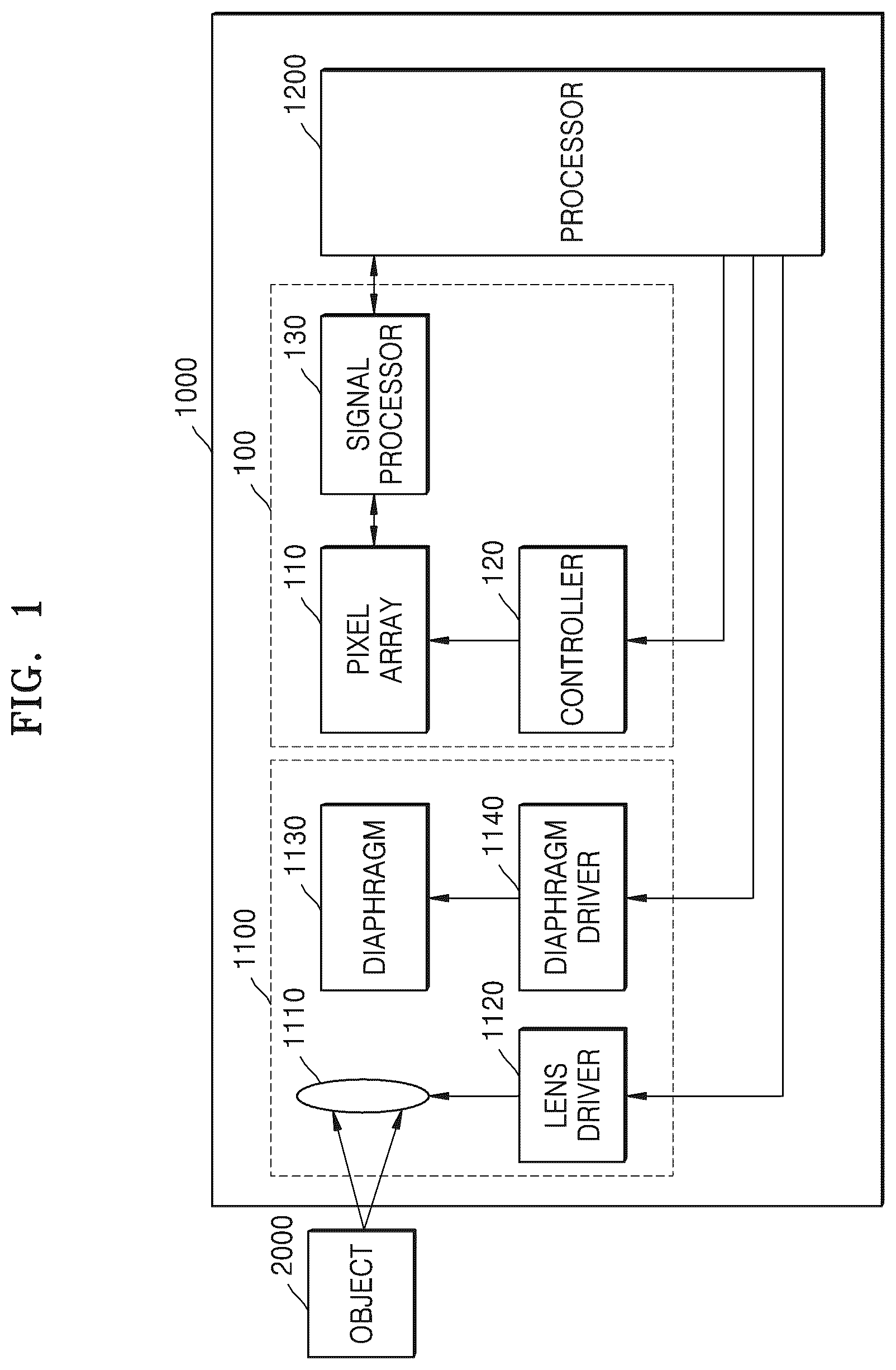
is a block diagram of a structure of a digital photography apparatus 1000 according to an embodiment of inventive concepts, for explaining execution of an auto-focus (AF) function of the digital photography apparatus 1000 .
The digital photography apparatus 1000 may include an imaging unit 1100 , an image sensor 100 , and a processor 1200 . The digital photography apparatus 1000 may include a focus detection function. The processor 1200 may be a hardware processor such as central processing unit (CPU), a multi-processor, a distributed processing system, an application specific integrated circuit (ASIC), and/or a suitable hardware processing unit, that when executing instructions according to firmware or software, configures the processor 1200 as a special purpose processor for controlling overall operations of the digital photography apparatus 1000 . The processor may include a memory (not shown). The memory may be a nonvolatile memory, such as a flash memory, a phase-change random access memory (PRAM), a magneto-resistive RAM (MRAM), a resistive RAM (ReRAM), or a ferro-electric RAM (FRAM), or a volatile memory, such as a static RAM (SRAM), a dynamic RAM (DRAM), or a synchronous DRAM (SDRAM).
Overall operations of the digital photography apparatus 1000 may be controlled by the processor 1200 . The processor 1200 may provide a lens driver 1120 , a diaphragm driver 1140 , a controller 120 , and the like with control signals for respectively driving them.
The imaging unit 1100 is a component for receiving light, and may include a lens 1110 , the lens driver 1120 , a diaphragm 1130 , and the diaphragm driver 1140 . The lens 1110 may include a plurality of lenses. The hardware for the lens driver 1120 and the diaphragm driver 1140 are not particularly limited and may include one or more known circuits for performing the respective functions of the lens driver 1120 and diaphragm driver 1140 discussed hereafter.
The lens driver 1120 may communicate with the processor 1200 through information about focus detection, and may adjust the location of the lens 1110 according to a control signal provided by the processor 1200 . The lens driver 1120 may move the lens 1110 in a direction in which a distance between the lens 1110 and an object 2000 increases or decreases. Accordingly, the distance between the lens 1110 and the object 2000 may be adjusted. The object 2000 may be focused or not focused according to a location of the lens 1110 .
For example, when the distance between the lens 1110 and the object 2000 is relatively small, the lens 1110 may deviate from an in-focus position for focusing the object 2000 , and a phase difference may occur between images formed on the image sensor 100 . The lens driver 1120 may move the lens 1110 in a direction in which the distance between the lens 1110 and the object 2000 increases, based on the control signal provided by the processor 1200 .
When the distance between the lens 1110 and the object 2000 is relatively large, the lens 1110 may deviate from the in-focus position, and a phase difference may occur between images formed on the image sensor 100 . The lens driver 1120 may move the lens 1110 in a direction in which the distance between the lens 1110 and the object 2000 decreases, based on the control signal provided by the processor 1200 .
The image sensor 100 may convert incident light into an image signal. The image sensor 100 may include a pixel array 110 , the controller 120 , and a signal processor 130 . An optical signal that has passed through the lens 1110 and the diaphragm 1130 may form an image of a subject when reaching a light-receiving surface of the pixel array 110 .
The pixel array 110 may be a complementary metal oxide semiconductor image sensor (CIS) which converts an optical signal to an electrical signal. Sensitivity or the like of the pixel array 110 may be controlled by the controller 120 . The pixel array 110 may include shared pixels for performing an AF function or a distance measuring function.
The processor 1200 may receive first pixel information and second pixel information from the signal processor 130 to perform a phase difference calculation, and the phase difference calculation may be achieved by performing a correlation operation on pixel signals of a plurality of shared pixels. The processor 1200 may obtain the position of a focus, the direction of the focus, or a distance between the object 2000 and the image sensor 100 , as a result of the phase difference calculation. The processor 1200 may output a control signal to the lens driver 1120 to move the location of the lens 1110 , based on the result of the phase difference calculation.
The processor 1200 may reduce noise in an input signal and may perform image signal processing for image quality improvement, such as gamma correction, color filter array interpolation, color matrix, color correction, or color enhancement. The processor 1200 may generate an image file by compressing image data obtained by performing the image signal processing for image quality improvement, or may restore the image data from the image file.
is a block diagram of a structure of the image sensor 100 according to an embodiment of inventive concepts.
Referring to , the image sensor 100 may include a pixel array 110 , a controller 120 , a signal processor 130 , a row driver 140 , and a signal reader 150 . The signal reader 150 may include a correlated double sampler (CDS) 151 , an analog-to-digital converter (ADC) 153 , and a buffer 155 .
The pixel array 110 may include a plurality of shared pixels SPX including first through fourth shared pixels SPX 1 through SPX 4 . The plurality of shared pixels SPX may generate image signals corresponding to an object. An example circuit for the first shared pixel SPX 1 and the second shared pixel SPX 2 will be described later with reference to .
Each of the plurality of shared pixels SPX may output a pixel signal to the CDS 151 via corresponding first through n-th column output lines CLO_ 0 through CLO_n−1. For example, the first shared pixel SPX 1 and the third shared pixel SPX 3 may be connected to the first column output line CLO_ 0 and provide pixel signals to the CDS 151 . The second shared pixel SPX 2 and the fourth shared pixel SPX 4 may be connected to the second column output line CLO_ 1 and provide pixel signals to the CDS 151 . However, inventive concepts are not limited thereto, and the first through fourth shared pixels SPX 1 through SPX 4 may be connected to different column output lines, respectively.
According to an embodiment, the first through fourth shared pixels SPX 1 through SPX 4 may be phase detection pixels, and the first through fourth shared pixels SPX 1 through SPX 4 may generate phase signals that are used to calculate a phase difference between images. The first through fourth shared pixels SPX 1 through SPX 4 may be used to focus an object. The phase signals may include information about the locations of images formed on the image sensor 100 , and may be used to calculate phase differences between the images. Based on the calculated phase differences, an in-focus position of the lens 1110 of may be calculated. For example, a position of the lens 1110 of that makes a phase difference be 0 may be the in-focus position.
The first through fourth shared pixels SPX 1 through SPX 4 may be used not only to focus the object but also to measure a distance between the object 2000 and the image sensor 100 . To measure the distance between the object 2000 and the image sensor 100 , additional pieces of information, such as phase differences between the images formed on the image sensor 100 , the distance between the lens 1110 and the image sensor 100 , the size of the lens 1110 , and the in-focus position of the lens 1110 , may be referred to.
Each of the plurality of shared pixels SPX may include a plurality of photo-sensing devices in a plurality of sub-pixels. According to an embodiment, each of the first through fourth shared pixels SPX 1 through SPX 4 may include four sub-pixels. Each of the plurality of sub-pixels may include a corresponding one of the plurality of photo-sensing devices, and the photo-sensing device included in each of the plurality of sub-pixels may absorb light and generate electric charges. For example, the photo-sensing device may be a photodiode.
The first shared pixel SPX 1 may include a plurality of photodiodes and a first floating diffusion region shared by the plurality of photodiodes of the first shared pixel SPX 1 . Similar to the above description of the first shared pixel SPX 1 , each of the second through fourth shared pixels SPX 2 through SPX 4 may include a plurality of photodiodes and a floating diffusion region shared by the plurality of photodiodes.
According to an embodiment, each of the first through fourth shared pixels SPX 1 through SPX 4 may include first pixel groups PXG 11 , PXG 21 , PXG 31 , and PXG 41 , respectively, and second pixel groups PXG 12 , PXG 22 , PXG 32 , and PXG 42 , respectively. A below description of the first pixel group PXG 11 and the second pixel group PXG 12 of the first shared pixel SPX 1 may be equally applied to the first pixel groups PXG 21 , PXG 31 , and PXG 41 and the second pixel groups PXG 22 , PXG 32 , and PXG 42 of the second through fourth shared pixel SPX 2 through SPX 4 .
According to an embodiment, each of the first pixel group PXG 11 and the second pixel group PXG 12 of the first shared pixel SPX 1 may include sub-pixels arranged side by side in a first direction, and the first pixel group PXG 11 and the second pixel group PXG 12 of the first shared pixel SPX 1 may be arranged side by side in a second direction. An AF function in the second direction may be performed based on a first pixel signal output by the first pixel group PXG 11 of the first shared pixel SPX 1 and a second pixel signal output by the second pixel group PXG 12 of the first shared pixel SPX 1 .
Alternatively, according to an embodiment, each of the first pixel group PXG 11 and the second pixel group PXG 12 of the first shared pixel SPX 1 may include sub-pixels arranged side by side in the second direction, and the first pixel group PXG 11 and the second pixel group PXG 12 of the first shared pixel SPX 1 may be arranged side by side in the first direction. An AF function in the first direction may be performed based on the first pixel signal output by the first pixel group PXG 11 of the first shared pixel SPX 1 and the second pixel signal output by the second pixel group PXG 12 of the first shared pixel SPX 1 .
According to an embodiment, sub-pixel regions in which the first pixel group PXG 11 included in the first shared pixel SPX 1 is formed may share a first well region doped with first conductivity type impurities (for example, n-type impurities), and sub-pixel regions in which the second pixel group PXG 12 included in the first shared pixel SPX 1 is formed may share a first well region doped with the first conductivity type impurities. Accordingly, even when the sub-pixel regions are miniaturized, because the first well region is formed over sub-pixel regions where one pixel group (for example, PXG 11 or PXG 12 ) is formed, a pattern of the first well region may relatively enlarge. In the image sensor 100 , the first well region may have a uniform pattern. In the image sensor 100 , the sub-pixel regions where one pixel group is formed are formed to share a first well region, and thus, the full well capacity (FWC) of the photo-sensing devices may increase.
According to an embodiment, an isolation layer may not be arranged between the sub-pixel regions in which the first pixel group PXG 11 included in the first shared pixel SPX 1 is formed, and an isolation layer may not be arranged between the sub-pixel regions in which the second pixel group PXG 12 included in the first shared pixel SPX 1 is formed. In other words, at least two sub-pixel regions may be formed within an isolation layer that forms a closed curve. Accordingly, the image sensor 100 has no isolation layers between the sub-pixel regions where one pixel group (for example, the first or second pixel group PXG 11 or PXG 12 ) is formed, and thus, light scattering due to an isolation layer may be limited and/or prevented and a light-receiving region may increase.
The controller 120 may control the row driver 140 so that the pixel array 110 absorbs light to accumulate electric charges or temporarily stores the accumulated electric charges and outputs electrical signals corresponding to the stored accumulated electric charges to the outside of the pixel array 110 . The controller 120 may also control the signal reader 150 to measure the level of a pixel signal provided by the pixel array 110 .
The row driver 140 may generate signals for controlling the pixel array 110 , namely, reset control signals RSs, transfer control signals TSs, and selection signals SELSs, and may provide the generated signals to the plurality of shared pixels SPX. According to an embodiment, the row driver 140 may determine activation and deactivation timing of the reset control signals RSs, the transfer control signals TSs, and the selection signals SELSs provided to the first through fourth shared pixels SPX 1 through SPX 4 , based on whether to perform an AF function or a distance measuring function.
The CDS 151 may sample and hold the pixel signal provided by the pixel array 110 . The CDS 151 may perform a double sampling on a level of certain noise and a level of the pixel signal to output a level corresponding to a difference between the level of the certain noise and the level of the pixel signal. In addition, the CDS 151 may receive a ramp signal generated by a ramp signal generator 157 , compare the ramp signal with the level corresponding to the difference between the level of the certain noise and the level of the pixel signal, and output a result of the comparison to the ADC 153 . The ADC 153 may convert an analog signal corresponding to the level of the result of the comparison received from the CDS 151 into a digital signal. The buffer 155 may latch the digital signal, and the latched digital signal may be sequentially output to the outside of the signal processor 130 or the image sensor 100 .
The signal processor 130 may perform signal processing, based on pixel signals of the first through fourth shared pixels SPX 1 through SPX 4 . For example, the signal processor 130 may perform noise reduction, gain adjustment, waveform shaping, interpolation, white balance adjustment, gamma correction, edge emphasis, and the like. The signal processor 130 may also perform a phase difference calculation for an AF operation by outputting signal-processed information to the processor 1200 during an AF operation. According to an embodiment, the signal processor 130 may be included in the processor 1200 of outside the image sensor 100 .
is a circuit diagram of the first shared pixel SPX 1 and the second shared pixel SPX 2 included in the pixel array 110 of , according to an embodiment of inventive concepts. Although two shared pixels, namely, the first shared pixel SPX 1 and the second shared pixel SPX 2 , are illustrated in , circuits of shared pixels other than the first shared pixel SPX 1 and the second shared pixel SPX 2 may be configured the same as the circuits of the first shared pixel SPX 1 and the second shared pixel SPX 2 illustrated in .
For convenience of explanation, only the first shared pixel SPX 1 will now be described. However, the description of the first shared pixel SPX 1 may be equally applied to the second shared pixel SPX 2 and the other shared pixels. For example, descriptions of a plurality of photo-sensing devices PD 11 through PD 14 , a plurality of transfer transistors TX 11 through TX 14 , a select transistor SX 1 , a drive transistor DX 1 , and a reset transistor RX 1 formed in the first shared pixel SPX 1 may be equally applied to a plurality of photo-sensing devices PD 21 through PD 24 , a plurality of transfer transistors TX 21 through TX 24 , a select transistor SX 2 , a drive transistor DX 2 , and a reset transistor RX 2 formed in the second shared pixel SPX 2 .
The first shared pixel SPX 1 may include the plurality of photo-sensing devices PD 11 through PD 14 , the plurality of transfer transistors TX 11 through TX 14 , the select transistor SX 1 , the drive transistor DX 1 , and the reset transistor RX 1 . According to an embodiment, at least one of the reset transistor RX 1 , the drive transistor DX 1 , and the select transistor SX 1 may be omitted. Although the first shared pixel SPX 1 includes the four photo-sensing devices PD 11 through PD 14 and the four transfer transistors TX 11 through TX 14 in , inventive concepts are not limited thereto. According to embodiments, the respective numbers of photo-sensing devices and transfer transistors included in the first shared pixel SPX 1 may vary.
Each of the photo-sensing devices PD 11 through PD 14 may generate a photocharge that varies according to the intensity of light. For example, the photo-sensing devices PD 11 through PD 14 are P-N junction diodes, and may generate electric charges, namely, electrons being negative charges and holes being positive charges, in proportion to the amount of incident light. Each of the photo-sensing devices PD 11 through PD 14 may be at least one of a photo transistor, a photo gate, a pinned photo diode (PDD), and a combination thereof.
The transfer transistors TX 11 through TX 14 may transfer the generated photocharges to a first floating diffusion region FD 1 , according to transfer control signals (for example, the transfer control signals TSs of ). When the transfer transistors TX 11 through TX 14 are turned on, the photocharges respectively generated by the photo-sensing devices PD 11 through PD 14 included in the first shared pixel SPX 1 may be transferred to the single first floating diffusion region FD 1 and may be accumulated and stored in the first floating diffusion region FD 1 .
The reset transistor RX 1 may periodically rest the electric charges accumulated in the first floating diffusion region FD 1 . A drain electrode of the reset transistor RX 1 may be connected to the first floating diffusion region FD 1 , and a source electrode thereof may be connected to a power supply voltage Vpix. When the reset transistor RX 1 is turned on according to reset control signals (for example, the reset control signals RSs of ), the power supply voltage Vpix connected to the source electrode of the reset transistor RX 1 is transmitted to the first floating diffusion region FD 1 . When the reset transistor RX 1 is turned on, electric charges accumulated in the first floating diffusion region FD 1 may be discharged, and thus, the first floating diffusion region FD 1 may be reset.
The drive transistor DX 1 may be controlled according to the number of photocharges accumulated in the first floating diffusion region FD 1 . The drive transistor DX 1 is a buffer amplifier, and thus, may buffer a signal corresponding to the electric charges accumulated in the first floating diffusion region FD 1 . The drive transistor DX 1 may amplify a change in a potential in the first floating diffusion region FD and may output the amplified potential change as a pixel signal Vout to the first column output line CLO_ 0 .
The select transistor SX 1 may have a drain terminal connected to a source terminal of the drive transistor DX 1 , and may output the pixel signal Vout to a CDS (for example, the CDS 151 of ) via the first column output line CLO_ 0 in response to selection signals (for example, the selection signals SELSs of ).
Each of the sub-pixels that constitute the first shared pixel SPX 1 may include a corresponding photo-sensing device (for example, one of the photo-sensing devices PD 11 through PD 14 ) and a corresponding transfer transistor (for example, one of the transfer transistors TX 11 through TX 14 ). For example, a first sub-pixel included in the first shared pixel SPX 1 may include the photo-sensing device PD 11 and the transfer transistor TX 11 , a second sub-pixel included in the first shared pixel SPX 1 may include the photo-sensing device PD 12 and the transfer transistor TX 12 , a third sub-pixel included in the first shared pixel SPX 1 may include the photo-sensing device PD 13 and the transfer transistor TX 13 , and a fourth sub-pixel included in the first shared pixel SPX 1 may include the photo-sensing device PD 14 and the transfer transistor TX 14 .
The sub-pixels that constitute the first shared pixel SPX 1 may share the first floating diffusion region FD 1 . The sharing by the first shared pixel SPX 1 may include not only the plurality of photo-sensing devices PD 1 through PD 4 sharing the single first floating diffusion region FD 1 but also sharing the reset transistor RX 1 , the drive transistor DX 1 , and the select transistor SX 1 except for the transfer transistors TX 1 through TX 4 .
is a schematic diagram of a pixel array of an image sensor according to an embodiment of inventive concepts, and illustrates a first pixel array 110 a included in the pixel array 110 of . In , first through fourth shared pixel regions SP 1 through SP 4 may mean at least respective portions of the regions where corresponding shared pixels (for example, the first through fourth shared pixels SPX 1 through SPX 4 of ) are formed, respectively. First group pixel regions PG 11 through PG 41 and second group pixel regions PG 12 through PG 42 may mean at least respective portions of the regions where corresponding group pixels (for example, PXG 11 , PXG 21 , PXG 31 , PXG 41 , PXG 12 , PXG 22 , PXG 32 , and PXG 42 of ) are respectively formed, and a plurality of sub-pixel regions, namely, first through fourth sub-pixel regions PX 11 through PX 14 , first through fourth sub-pixel regions PX 21 through PX 24 , first through fourth sub-pixel regions PX 31 through PX 34 , and first through fourth sub-pixel regions PX 41 through PX 44 , may mean at least respective portions of the regions where sub-pixels are respectively formed.
Referring to , the first pixel array 110 a may include the first through fourth sub-pixel regions PX 11 through PX 14 , the first through fourth sub-pixel regions PX 21 through PX 24 , the first through fourth sub-pixel regions PX 31 through PX 34 , and the first through fourth sub-pixel regions PX 41 through PX 44 arranged in a row direction (for example, the first direction X) and a column direction (for example, the second direction Y). According to an embodiment, a single shared pixel region may be defined as a unit including four sub-pixel regions arranged in two rows and two columns. Accordingly, the single shared pixel region may include four photo-sensing devices respectively formed in the four sub-pixel regions.
The first pixel array 110 a may include the first through fourth shared pixel regions SP 1 through SP 4 . The first pixel array 110 a may include a color filter such that the first through fourth shared pixel regions SP 1 through SP 4 may sense various colors. According to an embodiment, the color filter may include filters that sense red (R), green (G), and blue (B), and each of the first through fourth shared pixel regions SP 1 through SP 4 may include sub-pixel regions in which the same color is arranged.
According to an embodiment, the first through fourth shared pixel regions SP 1 through SP 4 may be arranged to correspond to a Bayer pattern, within the first pixel array 110 a . For example, the first shared pixel region SP 1 and the fourth shared pixel region SP 4 may include the first through fourth sub-pixel regions PX 11 through PX 14 and the first through fourth sub-pixel regions PX 41 through PX 44 including a green (G) color filter, the second shared pixel region SP 2 may include the first through fourth sub-pixel regions PX 21 through PX 24 including an red (R) color filter, and the third shared pixel region SP 3 may include the first through fourth sub-pixel regions PX 31 through PX 34 including a blue (B) color filter.
However, this is merely an embodiment, and thus, the first pixel array 110 a according an embodiment of inventive concepts may include various other types of color filters. For example, the color filter may include filters for sensing yellow, cyan, and magenta colors. Alternatively, the color filter may include filters for sensing red, green, blue and white colors. The first pixel array 110 a may include more shared pixel regions than those shown in and the first through fourth shared pixel regions SP 1 through SP 4 may be arranged in various layouts, and inventive concepts is not limited to the layout of .
According to an embodiment, in the first through fourth shared pixel regions SP 1 through SP 4 , the first pixel group regions PG 11 , PG 21 , PG 31 , and PG 41 and the second pixel group regions PG 12 , PG 22 , PG 32 , and PG 42 may be formed, respectively. For convenience of explanation, only the first shared pixel region SP 1 will now be described. However, the description of the first shared pixel region SP 1 may be equally applied to the second through fourth shared pixel regions SP 2 through SP 4 . For example, a description of the first pixel group region PG 11 of the first shared pixel region SP 1 is applicable to each of the first pixel group regions PG 21 , PG 31 , and PG 41 of the second through fourth shared pixel regions SP 2 through SP 4 , and a description of the second pixel group region PG 12 of the first shared pixel region SP 1 is applicable to each of the second pixel group regions PG 22 , PG 32 , and PG 42 of the second through fourth shared pixel regions SP 2 through SP 4 .
The first shared pixel region SP 1 may include the first pixel group region PG 11 including the first sub-pixel region PX 11 and the second sub-pixel region PX 12 arranged in a first row, and the second pixel group region PG 12 including the third sub-pixel region PX 13 and the fourth sub-pixel region PX 14 arranged in a second row. The first pixel group region PG 11 and the second pixel group region PG 12 of the first shared pixel region SP 1 may be arranged side by side in the second direction Y, which is a column direction.
The first sub-pixel region PX 11 and the second sub-pixel region PX 12 may share a first well region NW_X doped with first conductivity type impurities (for example, n-type impurities). The third sub-pixel region PX 13 and the fourth sub-pixel region PX 14 may share another first well region NW_X doped with first conductivity type impurities. The first well region NW_X formed in the first pixel group region PG 11 and the first well region NW_X formed in the second pixel group region PG 12 may be spaced apart from each other. The sub-pixels included in a single pixel group are formed to share the first well region NW_X, and thus respective FWCs of the first pixel group region PG 11 and the second pixel group region PG 12 may increase. When an image sensor is manufactured, a pattern of the first well region NW_X may relatively enlarge, and thus, the first well region NW_X may have a uniform pattern.
When the image sensor performs an AF function or a distance measuring function, transfer transistors TX 11 and TX 12 of the first sub-pixel region PX 11 and the second sub-pixel region PX 12 included in the first pixel group region PG 11 may be turned on together. Photocharges generated in a photo-sensing device PD 11 of the first sub-pixel region PX 11 and a photo-sensing device PD 12 of the second sub-pixel region PX 12 may be transmitted to a first floating diffusion region FD 1 , and a first pixel signal Vout 1 corresponding to the photocharges may be output to the first column output line CLO_ 0 .
When the image sensor performs an AF function or a distance measuring function, transfer transistors TX 13 and TX 14 of the third sub-pixel region PX 13 and the fourth sub-pixel region PX 14 included in the second pixel group region PG 12 may be turned on together. Photocharges generated in a photo-sensing device PD 13 of the third sub-pixel region PX 13 and a photo-sensing device PD 14 of the fourth sub-pixel region PX 14 may be transmitted to the first floating diffusion region FD 1 , and a second pixel signal Vout 2 corresponding to the photocharges may be output to the first column output line CLO_ 0 .
According to an embodiment, a processor (for example, the processor 1200 of ) may receive first pixel information corresponding to the first pixel signal Vout 1 output by each of the first pixel group regions PG 11 , PG 21 , PG 31 , and PG 41 of the first through fourth shared pixel regions SP 1 through SP 4 , and may receive second pixel information corresponding to the second pixel signal Vout 2 output by each of the second pixel group regions PG 12 , PG 22 , PG 32 , and PG 42 of the first through fourth shared pixel regions SP 1 through SP 4 . The processor 1200 may perform an AF operation of the second direction Y, which is a column direction, or a distance measuring operation of the second direction Y, by using the first pixel information and the second pixel information.
For example, the processor 1200 may calculate a phase difference by using first information UI and second information DI derived from Equation 1 below, and may perform an AF operation of the second direction Y or a distance measuring operation of the second direction Y. For example, the first information UI and the second information DI may mean upper information and lower information in the present drawing. UI=f ( V out_1_ PG 11, V out_1_ PG 21, V out_1_ PG 31, V out_1_ PG 41) DI=f ( V out_2_ PG 12, V out_2_ PG 22, V out_2_ PG 32, V out_2_ PG 42) [Equation 1]
where Vout_ 1 _PG 11 may be a first pixel signal output by the first pixel group region PG 11 of the first shared pixel region SP 1 , Vout_ 1 _PG 21 may be a first pixel signal output by the first pixel group region PG 21 of the second shared pixel region SP 2 , Vout_ 1 _PG 31 may be a first pixel signal output by the first pixel group region PG 31 of the third shared pixel region SP 3 , and Vout_ 1 _PG 41 may be a first pixel signal output by the first pixel group region PG 41 of the fourth shared pixel region SP 4 . In Equation 1, Vout_ 2 _PG 12 may be a second pixel signal output by the second pixel group region PG 12 of the first shared pixel region SP 1 , Vout_ 2 _PG 22 may be a second pixel signal output by the second pixel group region PG 22 of the second shared pixel region SP 2 , Vout_ 2 _PG 32 may be a second pixel signal output by the second pixel group region PG 32 of the third shared pixel region SP 3 , and Vout_ 2 _PG 42 may be a second pixel signal output by the second pixel group region PG 42 of the fourth shared pixel region SP 4 . A function f for deriving the first information UI and the second information DI may have various configurations.
The processor 1200 may not perform an AF operation of the second direction Y or a distance measuring operation of the second direction Y by using pixel signals respectively output by sub-pixels, but may perform an AF operation of the second direction Y or a distance measuring operation of the second direction Y by using pixel signals respectively output by group pixels. The number of calculations performed by the processor 1200 to accomplish an AF operation of the second direction Y or a distance measuring operation of the second direction Y may be reduced.
A and 5 B illustrate a pixel array of an image sensor according to an embodiment of inventive concepts, wherein A is a cross-sectional view taken along line X 1 -X 2 of and B is a cross-sectional view taken along line Y 1 -Y 2 of .
Referring to , 5 A, and 5 B , a semiconductor substrate 111 , on which the first through fourth sub-pixel regions PX 11 through PX 14 , the first through fourth sub-pixel regions PX 21 through PX 24 , the first through fourth sub-pixel regions PX 31 through PX 34 , and the first through fourth sub-pixel regions PX 41 through PX 44 are formed, may be provided. The semiconductor substrate 111 may have a first surface 111 f and a second surface 111 b opposite to each other. For example, the first surface 111 f may be a front surface of the semiconductor substrate 111 , and the second surface 111 b may be a rear surface of the semiconductor substrate 111 . Circuits may be arranged on the first surface 111 f , and light may be incident upon the second surface 111 b.
According to an embodiment, the semiconductor substrate 111 may be, but is not limited to, a silicon epitaxial layer doped with second conductivity type impurities (for example, p-type impurities). A and 5 B illustrate a photo-sensing region in which a photo-sensing device is formed, but a transfer transistor and the like may be further formed in the photo-sensing region.
Photo-sensing regions 113 may be arranged within the semiconductor substrate 111 . A single photo-sensing region 113 may be formed in each of the first through fourth sub-pixel regions PX 11 through PX 14 , the first through fourth sub-pixel regions PX 21 through PX 24 , the first through fourth sub-pixel regions PX 31 through PX 34 , and the first through fourth sub-pixel regions PX 41 through PX 44 . For example, a single photo-sensing region 113 may be formed in each of the first sub-pixel region PX 11 , the second sub-pixel region PX 12 , the third sub-pixel region PX 13 , and the fourth sub-pixel region PX 14 of the first shared pixel region SP 1 . The photo-sensing regions 113 may be arranged in the first direction X and the second direction Y to form a matrix, from a planar viewpoint.
The photo-sensing regions 113 may be formed by ion-implanting impurities of a first conductivity type (for example, an n type) into the semiconductor substrate 111 . According to an embodiment, photo-sensing devices, namely, photodiodes, may be formed due to junction of the photo-sensing regions 113 of a first conductivity type and the semiconductor substrate 111 of a second conductivity type. However, inventive concepts are not limited thereto, and photo-sensing devices may be formed due to junction of another component doped with the second conductivity type impurities and the photo-sensing regions 113 of the first conductivity type.
The first well region NW_X having the first conductivity type may be formed on the photo-sensing regions 113 . The first well region NW_X may be formed by ion-implanting impurities of the first conductivity type into the semiconductor substrate 111 . A doping concentration of the first well region NW_X may be lower than that of the photo-sensing regions 113 . Because the photo-sensing regions 113 may receive electric charges from the first well region NW_X, FWCs of the photo-sensing regions 113 may increase.
The first well region NW_X may be formed over the sub-pixel regions included in the same pixel group region. For example, a single first well region NW_X may be formed over the first sub-pixel region PX 11 and the second sub-pixel region PX 12 included in the first pixel group region PG 11 of the first shared pixel region SP 1 . Sub-pixel regions included in different pixel groups may include first well regions NW_X spaced apart from each other, respectively. Electric charges generated in the first sub-pixel region PX 11 and electric charges generated in the second sub-pixel region PX 12 may move between each other via the first well region NW_X.
A separation impurity layer 115 may be formed by ion-implanting impurities of a second conductivity type into the semiconductor substrate 111 . A concentration of the second conductivity type impurities in the separation impurity layer 115 may be greater than that in the semiconductor substrate 111 . The separation impurity layer 115 may include first portions each extending in the first direction X and second portions each extending in the second direction Y, and, for example, may be formed in a lattice shape.
The separation impurity layer 115 may surround the photo-sensing regions 113 . For example, the separation impurity layer 115 may be formed between photo-sensing regions 113 adjacent to each other in the first direction X, and the separation impurity layers 115 may be formed between photo-sensing regions 113 adjacent to each other in the second direction Y.
The separation impurity layer 115 having an opposite conductivity type to the photo-sensing regions 113 may provide a potential barrier between the photo-sensing regions 113 . In other words, potential wells may be formed in the photo-sensing regions 113 by the separation impurity layer 115 . The photo-sensing regions 113 may be separated from each other by the separation impurity layer 115 .
First isolation layers 117 _ 1 and second isolation layers 117 _ 2 may be formed within the semiconductor substrate 111 . According to an embodiment, the first isolation layers 117 _ 1 and the second isolation layers 117 _ 2 may each extend perpendicularly from the second surface 111 b of the semiconductor substrate 111 . According to an embodiment, the first isolation layers 117 _ 1 and the second isolation layers 117 _ 2 may each extend perpendicularly from the first surface 111 f of the semiconductor substrate 111 . The first isolation layers 117 _ 1 and the second isolation layers 117 _ 2 may have various shapes and may be manufactured according to various processes.
According to an embodiment, the first isolation layers 117 _ 1 may be formed to have greater widths than the second isolation layers 117 _ 2 . According to an embodiment, the first isolation layers 117 _ 1 may be formed more deeply than the second isolation layers 117 _ 2 . However, inventive concepts are not limited thereto, and the first isolation layers 117 _ 1 and the second isolation layers 117 _ 2 may have the same shapes and may be formed via the same process.
The first isolation layers 117 _ 1 and the second isolation layers 117 _ 2 may be formed of an insulating material having a lower refractive index than that of a material used to form the semiconductor substrate 111 . For example, the first isolation layers 117 _ 1 and the second isolation layers 117 _ 2 may include silicon oxide, silicon nitride, undoped polysilicon, air, or a combination thereof.
The first isolation layers 117 _ 1 and the second isolation layers 117 _ 2 may refract incident light that is incident upon sub-pixel regions. The first isolation layers 117 _ 1 and the second isolation layers 117 _ 2 may limit and/or prevent photocharges generated from the incident light from moving to adjacent sub-pixel regions due to random drift.
The first isolation layers 117 _ 1 may be formed to surround each of the first through fourth shared pixel regions SP 1 through SP 4 . In other words, the first isolation layers 117 _ 1 may define a single shared pixel region. For example, a first isolation layer 117 _ 1 extending in the second direction Y may be formed between the first shared pixel region SP 1 and the second shared pixel region SP 2 , and a first isolation layer 117 _ 1 extending in the first direction X may be formed between the first shared pixel region SP 1 and the third shared pixel region SP 3 .
The second isolation layers 117 _ 2 may be formed within the first through fourth shared pixel regions SP 1 through SP 4 . Each second isolation layer 117 _ 2 may be formed between different sub-pixel regions. For example, a second isolation layer 117 _ 2 extending in the second direction Y may be formed between the first sub-pixel region PX 11 and the second sub-pixel region PX 12 of the first shared pixel region SP 1 , and a second isolation layer 117 _ 2 extending in the first direction X may be formed between the first sub-pixel region PX 11 and the third sub-pixel region PX 13 of the first shared pixel region SP 1 .
According to an embodiment, the second isolation layers 117 _ 2 may not be formed between sub-pixel regions included in the same pixel group, and the second isolation layers 117 _ 2 may be formed between sub-pixel regions included in different pixel groups. For example, no second isolation layers 117 _ 2 may be formed between the first sub-pixel region PX 11 and the second sub-pixel region PX 12 included in the first pixel group region PG 11 of the first shared pixel region SP 1 .
Color filter layers GCF, RCF, and BCF and micro-lenses ML may be arranged on the second surface 111 b of the semiconductor substrate 111 . Green color filter layers GCF may be arranged in the first shared pixel region and the fourth shared pixel region, a red color filter layer RCF may be arranged in the second shared pixel region, and a blue color filter layer BCF may be arranged in the third shared pixel region. In other words, the same color filter layers may be arranged in the sub-pixel regions included in the same shared pixel region.
The color filter layers GCF, RCF, and BCF may be formed to correspond to the sub-pixel regions, and the microlenses ML may also be formed to correspond to the sub-pixel regions. For example, the sub-pixel regions may include different microlenses ML, respectively.
illustrates a pixel array of an image sensor according to an embodiment of inventive concepts, and is a cross-sectional view taken along line X 1 -X 2 of . Reference numerals of that are the same as those of A will not be described again here.
Referring to , the color filter layers GCF, RCF, and BCF and micro-lenses ML′ may be arranged on the second surface 111 b of the semiconductor substrate 111 . According to an embodiment, each microlens ML′ may be formed to correspond to each pixel group region. For example, a single microlens ML′ may be arranged in the first pixel group region PG 11 of the first shared pixel region SP 1 , and a single microlens ML′ may be arranged in the second pixel group region PG 12 of the first shared pixel region SP 1 . In this case, a microlens MU that is different from the microlens ML′ of the first pixel group region PG 11 may be arranged in the second pixel group region PG 12 of the first shared pixel region SP 1 .
According to an embodiment, each microlens ML′ may be formed to correspond to each shared pixel region. For example, a single microlens MU may be arranged in each of the first through fourth shared pixel regions SP 1 through SP 4 .
is a schematic diagram of a pixel array of an image sensor according to an embodiment of inventive concepts, and illustrates a second pixel array 110 b included in the pixel array 110 of .
Referring to , the second pixel array 110 b may include first through fourth shared pixel regions SP 1 b through SP 4 b . Each of the first through fourth shared pixel regions SP 1 b through SP 4 b may include sub-pixel regions in which the same color filter is arranged.
According to an embodiment, in the first through fourth shared pixel regions SP 1 b through SP 4 b , first pixel group regions PG 11 b , PG 21 b , PG 31 b , and PG 41 b and second pixel group regions PG 12 b , PG 22 b , PG 32 b , and PG 42 b may be formed, respectively. For convenience of explanation, only the first shared pixel region SP 1 b will now be described. However, the description of the first shared pixel region SP 1 b may be equally applied to the second through fourth shared pixel regions SP 2 b through SP 4 b.
The first shared pixel region SP 1 b may include the first pixel group region PG 11 b including a first sub-pixel region PX 11 b and a third sub-pixel region PX 13 b arranged in a first column, and the second pixel group region PG 12 b including a second sub-pixel region PX 12 b and a fourth sub-pixel region PX 14 b arranged in a second column. The first pixel group region PG 11 b and the second pixel group region PG 12 b of the first shared pixel region SP 1 b may be arranged side by side in the first direction X, which is a row direction.
The first sub-pixel region PX 11 b and the third sub-pixel region PX 13 b may share a first well region NW_Y doped with first conductivity type impurities (for example, n-type impurities). The second sub-pixel region PX 12 b and the fourth sub-pixel region PX 14 b may share another first well region NW_Y doped with first conductivity type impurities. The first well region NW_Y formed in the first pixel group region PG 11 b and the first well region NW_Y formed in the second pixel group region PG 12 b may be apart from each other. Accordingly, the sub-pixels included in a single pixel group region (PG 11 b or PG 12 b ) are formed to share the first well region NW_Y, and thus, respective FWCs of the first pixel group region PG 11 b and the second pixel group region PG 12 b may increase.
When the image sensor performs an AF function or a distance measuring function, transfer transistors TX 11 and TX 13 of the first sub-pixel region PX 11 b and the third sub-pixel region PX 13 b included in the first pixel group region PG 11 b may be turned on together. Photocharges generated in a photo-sensing device PD 11 of the first sub-pixel region PX 11 b and a photo-sensing device PD 13 of the third sub-pixel region PX 13 b may be transmitted to a first floating diffusion region FD 1 , and a first pixel signal (for example, the first pixel signal Vout 1 of ) corresponding to the photocharges may be output to a first column output line (for example, the first column output line CLO_ 0 of ).
When the image sensor performs an AF function or a distance measuring function, transfer transistors TX 12 and TX 14 of the second sub-pixel region PX 12 b and the fourth sub-pixel region PX 14 b included in the second pixel group region PG 12 b may be turned on together. Photocharges generated in a photo-sensing device PD 12 of the second sub-pixel region PX 12 b and a photo-sensing device PD 14 of the fourth sub-pixel region PX 14 b may be transmitted to the first floating diffusion region FD 1 , and a second pixel signal (for example, the second pixel signal Vout 2 of ) corresponding to the photocharges may be output to the first column output line CLO_ 0 .
According to an embodiment, a processor (for example, the processor 1200 of ) may receive first pixel information corresponding to the first pixel signal Vout 1 output by each of the first pixel group regions PG 11 b , PG 21 b , PG 31 b , and PG 41 b of the first through fourth shared pixel regions SP 1 b through SP 4 b , and may receive second pixel information corresponding to the second pixel signal Vout 2 output by each of the second pixel group regions PG 12 b , PG 22 b , PG 32 b , and PG 42 b of the first through fourth shared pixel regions SP 1 b through SP 4 b . The processor 1200 may perform an AF operation of the first direction X, which is a row direction, or a distance measuring operation of the first direction X, by using the first pixel information and the second pixel information.
For example, the processor 1200 may calculate a phase difference by using third information LI and fourth information RI derived from Equation 2 below, and may perform an AF operation of the first direction X or a distance measuring operation of the first direction X. For example, the third information LI and the fourth information RI may mean left information and right information in the present drawing. LI=f ( V out_1_ PG 11 b,V out_1_ PG 21 b,V out_1_ PG 31 b,V out_1_ PG 41 b ) RI=f ( V out_2_ PG 12 b,V out_2_ PG 22 b,V out_2_ PG 32 b,V out_2_ PG 42 b ) [Equation 2]
where Vout_ 1 _PG 11 b may be a first pixel signal output by the first pixel group region PG 11 b of the first shared pixel region SP 1 b , Vout_ 1 _PG 21 b may be a first pixel signal output by the first pixel group region PG 21 b of the second shared pixel region SP 2 b , Vout_ 1 _PG 31 b may be a first pixel signal output by the first pixel group region PG 31 b of the third shared pixel region SP 3 b , and Vout_ 1 _PG 41 b may be a first pixel signal output by the first pixel group region PG 41 b of the fourth shared pixel region SP 4 b . In Equation 2, Vout_ 2 _PG 12 b may be a second pixel signal output by the second pixel group region PG 12 b of the first shared pixel region SP 1 b , Vout_ 2 _PG 22 b may be a second pixel signal output by the second pixel group region PG 22 b of the second shared pixel region SP 2 b , Vout_ 2 _PG 32 b may be a second pixel signal output by the second pixel group region PG 32 b of the third shared pixel region SP 3 b , and Vout_ 2 _PG 42 b may be a second pixel signal output by the second pixel group region PG 42 b of the fourth shared pixel region SP 4 b . A function f for deriving the third information LI and the fourth information RI may have various configurations.
The processor 1200 may not perform an AF operation of the first direction X or a distance measuring operation of the first direction X by using pixel signals respectively output by sub-pixels, but may perform an AF operation of the first direction X or a distance measuring operation of the first direction X by using pixel signals respectively output by group pixels. The number of calculations performed by the processor 1200 to accomplish an AF operation of the first direction X or a distance measuring operation of the first direction X may be reduced.
According to an embodiment, a pixel array (for example, the pixel array 110 of ) of an image sensor may include both the first pixel array 110 a of and the second pixel array 110 b of , and the image sensor may perform respective AF functions of the first direction X and the second direction Y or respective distance measuring functions of the first direction X and the second direction Y. According to an embodiment, a pixel array of an image sensor according to inventive concepts may include the first pixel array 110 a and the second pixel array 110 b arranged adjacent to each other.
is a schematic diagram of a pixel array of an image sensor according to an embodiment of inventive concepts, and illustrates a third pixel array 110 c included in the pixel array 110 of . A and 9 B illustrate a pixel array of an image sensor according to an embodiment of inventive concepts, wherein A is a cross-sectional view taken along line X 3 -X 4 of and B is a cross-sectional view taken along line Y 3 -Y 4 of . The same reference characters and numerals in A and 9 B as those in A and 5 B denote the same elements, and thus their description will be omitted herein.
Referring to , 9 A, and 9 B , the third pixel array 110 c may include first through fourth shared pixel regions SP 1 c through SP 4 c . Each of the first through fourth shared pixel regions SP 1 c through SP 4 c may include sub-pixel regions in which the same color filter is arranged.
According to an embodiment, in the first through fourth shared pixel regions SP 1 c through SP 4 c , first pixel group regions PG 11 c , PG 21 c , PG 31 c , and PG 41 c and second pixel group regions PG 12 c , PG 22 c , PG 32 c , and PG 42 c may be formed, respectively. For convenience of explanation, only the first shared pixel region SP 1 c will now be described. However, the description of the first shared pixel region SP 1 c may be equally applied to the second through fourth shared pixel regions SP 2 c through SP 4 c.
The first shared pixel region SP 1 c may include the first pixel group region PG 11 c including a first sub-pixel region PX 11 c and a second sub-pixel region PX 12 c arranged in a first row, and the second pixel group region PG 12 c including a third sub-pixel region PX 13 c and a fourth sub-pixel region PX 14 c arranged in a second row. The first pixel group region PG 11 c and the second pixel group region PG 12 c of the first shared pixel region SP 1 c may be arranged side by side in the second direction Y, which is a column direction. Accordingly, a processor (for example, the processor 1200 of ) may perform an AF operation of the second direction Y, based on a first pixel signal (for example, the first pixel signal Vout 1 of ) output by the first pixel group region PG 11 c and a second pixel signal (for example, the second pixel signal Vout 2 of ) output by the second pixel group region PG 12 c.
Second well regions PW_X having a second conductivity type (for example, a p type) may be formed on separation impurity layers 115 . The second well regions PW_X may be formed by ion-implanting impurities of the second conductivity type into the semiconductor substrate 111 . A doping concentration of the second well regions PW_X may be lower than that of the separation impurity layers 115 .
A second well region PW_X may be formed to surround the first pixel group region PG 11 c and the second pixel group region PG 12 c . In other words, the second well region PW_X may be formed on a boundary region that surrounds center regions of the first pixel group region PG 11 c and the second pixel group region PG 12 c , and may be spaced apart from the center regions of the first pixel group region PG 11 c and the second pixel group region PG 12 c . In other words, the second well region PW_X may not be formed on the center regions of the first pixel group region PG 11 c and the second pixel group region PG 12 c.
Although not shown in A, and 9 B , according to an embodiment, a first well region (for example, the first well region NW_X of A ) having the first conductivity type (for example, n-type impurities) may be formed on the photo-sensing regions 113 . The first well region may be formed over the sub-pixel regions included in the same pixel group region. For example, a single first well region may be formed over the first sub-pixel region PX 11 c and the second sub-pixel region PX 12 included in the first pixel group region PG 11 c of the first shared pixel region SP 1 c . Alternatively, N-type well region may be formed in each of subpixel regions included in the same pixel group region.
In contrast with the , 9 A, and 9 B , the first shared pixel region SP 1 c may include a first pixel group region including the first sub-pixel region PX 11 c and the third sub-pixel region PX 13 c arranged in a first column, and a second pixel group region including the second sub-pixel region PX 12 c and the fourth sub-pixel region PX 14 c arranged in a second column. In this case, the first pixel group region and the second pixel group region of the first shared pixel region SP 1 c may be arranged side by side in the first direction X, which is a row direction. In this case, the processor 1200 of may perform an AF operation of the first direction X, based on a first pixel signal (for example, the first pixel signal Vout 1 of ) output by the first pixel group region and a second pixel signal (for example, the second pixel signal Vout 2 of ) output by the second pixel group region.
is a schematic diagram of a pixel array of an image sensor according to an embodiment of inventive concepts, and illustrates a fourth pixel array 110 d included in the pixel array 110 of . A and 11 B illustrate a pixel array of an image sensor according to an embodiment of inventive concepts, wherein A is a cross-sectional view taken along line X 5 -X 6 of and B is a cross-sectional view taken along line Y 5 -Y 6 of . The same reference characters and numerals in A and 11 B as those in A and 5 B denote the same elements, and thus their description will be omitted herein.
Referring to , 11 A, and 11 B , the fourth pixel array 110 d may include first through fourth shared pixel regions SP 1 d through SP 4 d . Each of the first through fourth shared pixel regions SP 1 d through SP 4 d may include sub-pixel regions in which the same color filter is arranged.
According to an embodiment, in the first through fourth shared pixel regions SP 1 d through SP 4 d , first pixel group regions PG 11 d , PG 21 d , PG 31 d , and PG 41 d and second pixel group regions PG 12 d , PG 22 d , PG 32 d , and PG 42 d may be formed, respectively. For convenience of explanation, only the first shared pixel region SP 1 d will now be described. However, the description of the first shared pixel region SP 1 d may be equally applied to the second through fourth shared pixel regions SP 2 d through SP 4 d.
The first shared pixel region SP 1 d may include the first pixel group region PG 11 d including a first sub-pixel region PX 11 d and a second sub-pixel region PX 12 d arranged in a first row, and the second pixel group region PG 12 d including a third sub-pixel region PX 13 d and a fourth sub-pixel region PX 14 d arranged in a second row. The first pixel group region PG 11 d and the second pixel group region PG 12 d of the first shared pixel region SP 1 d may be arranged side by side in the second direction Y, which is a column direction.
A first isolation layer 117 _ 1 and a second isolation layer 117 _ 2 X may be formed within the semiconductor substrate 111 . The first isolation layers 117 _ 1 may be formed to surround the first shared pixel region SP 1 d . In other words, the first isolation layer 117 _ 1 may define a single shared pixel region.
The second isolation layer 117 _ 2 X may be formed within the first through fourth shared pixel regions SP 1 d through SP 4 d . According to an embodiment, the second isolation layer 117 _ 2 X extending in the first direction X may be formed between the first pixel group region PG 11 d and the second pixel group region PG 12 d . The second isolation layer 117 _ 2 X may not be formed inside the first pixel group region PG 11 c and inside the second pixel group region PG 12 c , for example, on center regions of the first pixel group region PG 11 c and the second pixel group region PG 12 c . In other words, at least two sub-pixel regions (for example, the first sub-pixel region PX 11 d and the second sub-pixel region PX 12 d ) may be arranged within a closed curved surface formed by the first isolation layer 117 _ 1 and the second isolation layer 117 _ 2 X.
Because the fourth pixel array 110 d does not include the second isolation layer 117 _ 2 X inside a pixel group region, namely, a center region of the pixel group region, light scattering due to the second isolation layer 117 _ 2 X may be limited and/or prevented. In addition, a light-receiving region of the sub-pixel regions (for example, the first and second sub-pixel regions PX 11 d and PX 12 d ) included in a single pixel group region (for example, the first pixel group region PG 11 d ) may increase.
According to an embodiment, the first isolation layer 117 _ 1 may be formed to have a greater width than the second isolation layer 117 _ 2 X. In other words, a first width w 1 of the first isolation layer 117 _ 1 may be greater than a second width w 2 of the second isolation layer 117 _ 2 X. According to an embodiment, the first isolation layer 117 _ 1 may be formed more deeply than the second isolation layer 117 _ 2 X. In other words, a first depth d 1 of the first isolation layer 117 _ 1 from one surface (for example, the second surface 111 b ) of the semiconductor substrate 111 may be greater than a second depth d 2 of the second isolation layer 117 _ 2 X from the surface (for example, the second surface 111 b ) of the semiconductor substrate 111 . Because the first width w 1 of the first isolation layer 117 _ 1 formed between shared pixel regions is relatively large and the first depth d 1 of the first isolation layer 117 _ 1 is relatively large, occurrence of cross-talk between the shared pixel regions may be limited and/or prevented.
According to an embodiment, a first well region (for example, the first well region NW_X of A ) having the first conductivity type may be formed on the photo-sensing regions 113 . The first well region may be formed over the sub-pixel regions included in the same pixel group region. For example, a single first well region NW_X may be formed over the first sub-pixel region PX 11 d and the second sub-pixel region PX 12 d included in the first pixel group region PG 11 d of the first shared pixel region SP 1 d . A second well region (for example, the second well region PW_X of B ) having the second conductivity type may be further formed on the separation impurity layer 115 . The second well region PW_X may be formed to surround each of the first pixel group region PG 11 d and the second pixel group region PG 12 d.
According to an embodiment, a processor (for example, the processor 1200 of ) may receive first pixel information corresponding to a first pixel signal Vout 1 output by each of the first pixel group regions PG 11 d , PG 21 d , PG 31 d , and PG 41 d of the first through fourth shared pixel regions SP 1 d through SP 4 d , and may receive second pixel information corresponding to a second pixel signal Vout 2 output by each of the second pixel group regions PG 12 d , PG 22 d , PG 32 d , and PG 42 d of the first through fourth shared pixel regions SP 1 d through SP 4 d . The processor 1200 may perform an AF operation of the second direction Y, which is a column direction, or a distance measuring operation of the second direction Y, by using the first pixel information and the second pixel information.
is a schematic diagram of a pixel array of an image sensor according to an embodiment of inventive concepts, and illustrates a fifth pixel array 110 e included in the pixel array 110 of .
Referring to , the fifth pixel array 110 e may include first through fourth shared pixel regions SP 1 e through SP 4 e . Each of the first through fourth shared pixel regions SP 1 e through SP 4 e may include sub-pixel regions in which the same color filter is arranged.
According to an embodiment, in the first through fourth shared pixel regions SP 1 e through SP 4 e , first pixel group regions PG 11 e , PG 21 e , PG 31 e , and PG 41 e and second pixel group regions PG 12 e , PG 22 e , PG 32 e , and PG 42 e may be formed, respectively. For convenience of explanation, only the first shared pixel region SP 1 e will now be described. However, the description of the first shared pixel region SP 1 e may be equally applied to the second through fourth shared pixel regions SP 2 e through SP 4 e.
The first shared pixel region SP 1 e may include the first pixel group region PG 11 e including a first sub-pixel region PX 11 e and a third sub-pixel region PX 13 e arranged in a first column, and the second pixel group region PG 12 e including a second sub-pixel region PX 12 e and a fourth sub-pixel region PX 14 e arranged in a second column. The first pixel group region PG 11 e and the second pixel group region PG 12 e of the first shared pixel region SP 1 e may be arranged side by side in the first direction X, which is a row direction.
A first isolation layer 117 _ 1 and a second isolation layer 117 _ 2 Y may be formed within the fifth pixel array 110 e . The second isolation layer 117 _ 2 Y may be formed within the first through fourth shared pixel regions SP 1 e through SP 4 e . According to an embodiment, the second isolation layer 117 _ 2 Y extending in the second direction Y may be formed between the first pixel group region PG 11 e and the second pixel group region PG 12 e . The second isolation layer 117 _ 2 Y may not be formed on a center region of the first pixel group region PG 11 e and a center region of the second pixel group region PG 12 e . In other words, at least two sub-pixel regions (for example, the first sub-pixel region PX 11 e and the second sub-pixel region PX 12 e ) may be arranged within a closed curved surface formed by the first isolation layer 117 _ 1 and the second isolation layer 117 _ 2 Y.
According to an embodiment, the first isolation layer 117 _ 1 may be formed to have a greater width than the second isolation layer 117 _ 2 Y. According to an embodiment, the first isolation layer 117 _ 1 may be formed more deeply than the second isolation layer 117 _ 2 Y.
According to an embodiment, a processor (for example, the processor 1200 of ) may receive first pixel information corresponding to a first pixel signal Vout 1 output by each of the first pixel group regions PG 11 e , PG 21 e , PG 31 e , and PG 41 e of the first through fourth shared pixel regions SP 1 e through SP 4 e , and may receive second pixel information corresponding to a second pixel signal Vout 2 output by each of the second pixel group regions PG 12 e , PG 22 e , PG 32 e , and PG 42 e of the first through fourth shared pixel regions SP 1 e through SP 4 e . The processor 1200 may perform an AF operation of the first direction X, which is a row direction, or a distance measuring operation of the first direction X, by using the first pixel information and the second pixel information.
According to an embodiment, a pixel array (for example, the pixel array 110 of ) of an image sensor may include both the fourth pixel array 110 d of and the fifth pixel array 110 e of . Accordingly, the image sensor may perform respective AF functions of the first direction X and the second direction Y. According to an embodiment, the pixel array 110 of the image sensor may include the fourth pixel array 110 d and the fifth pixel array 110 e arranged adjacent to each other.
While inventive concepts have been particularly shown and described with reference to embodiments thereof, it will be understood that various changes in form and details may be made therein without departing from the spirit and scope of the following claims.
Figures (15)
Citations
This patent cites (27)
- US6937270
- US7381936
- US7646403
- US7916362
- US8716769
- US9398205
- US9578223
- US10177182
- US10424609
- US10998365
- US11282875
- US2010/0006969
- US2010/0225252
- US2010/0230583
- US2013/0049082
- US2014/0054662
- US2015/0319420
- US2017/0047363
- US2017/0053962
- US2017/0104020
- US2018/0286897
- US2019/0131333
- US2019/0172868
- US2020/0075660
- US2020/0127037
- US2006-173634
- US10-2018-0051145