Abstract
An electronic device and a diode are provided. The electronic device includes a switch circuit and a diode. The switch circuit includes a transistor. The diode has a first pin and a second pin. The first pin is electrically coupled to the transistor. The second pin is an idle contact.
Claims (17)
1. An electronic device, comprising: a switch circuit, comprising: a transistor; and a diode, having a first pin, a second pin, a third pin and a fourth pin, wherein the first pin is electrically coupled to the transistor, and the second pin is an idle contact, wherein the first pin, the second pin, the third pin, and the fourth pin are disposed in a point-symmetrical manner, wherein: the first pin and the third pin are disposed substantially in a diagonal manner across the diode, and the second pin and the fourth pin are disposed substantially in a diagonal manner across the diode.
11. A diode, comprising: a first pin; a second pin; a third pin; and a fourth pin, wherein the first pin, the second pin, the third pin, and the fourth pin are disposed in a point symmetrical manner, wherein: the first pin and the third pin are disposed substantially in a diagonal manner across the diode, and the second pin and the fourth pin are disposed substantially in a diagonal manner across the diode.
Show 15 dependent claims
2. The electronic device according to claim 1 , wherein: the transistor has a first terminal and a second terminal, the first terminal is a gate electrode, the second terminal is a source electrode, and the second terminal is electrically coupled to the first pin.
3. The electronic device according to claim 1 , wherein the diode further has a first positive electrode and a first negative electrode, the first negative electrode corresponds to the first pin, and the first positive electrode corresponds to the third pin.
4. The electronic device according to claim 1 , wherein the third pin is further coupled to an operating voltage.
5. The electronic device according to claim 4 , wherein the operating voltage is greater than a voltage at the first terminal of the transistor.
6. The electronic device according to claim 1 , wherein: the diode further has a first side and a second side, the first side and the second side are opposite to each other, the first pin and the fourth pin are disposed on the first side, and the second pin and the third pin are disposed on the second side.
7. The electronic device according to claim 6 , wherein: the diode further has a third side and a fourth side, the third side and the fourth side are opposite to each other, the first pin is spaced from the third side by a first distance along an extension direction of the first side, and the third pin is spaced from the fourth side by the first distance along an extension direction of the second side.
8. The electronic device according to claim 7 , wherein: the second pin is spaced from the third side by a second distance along the extension direction of the second side, and the fourth pin is spaced from the fourth side by the second distance along the extension direction of the first side.
9. The electronic device according to claim 1 , wherein: the diode further has a first capacitor and a second capacitor, the first capacitor corresponds to the fourth pin, and the second capacitor corresponds to the second pin.
10. The electronic device according to claim 1 , wherein the transistor is a PMOS field effect transistor.
12. The diode according to claim 11 , further comprising a first capacitor and a second capacitor, wherein the first capacitor corresponds to the fourth pin, and the second capacitor corresponds to the second pin.
13. The diode according to claim 11 , wherein: the diode further comprises a first side and a second side, the first side and the second side are opposite to each other, the first pin and the fourth pin are disposed on the first side, and the second pin and the third pin are disposed on the second side.
14. The diode according to claim 13 , wherein: the diode further comprises a third side and a fourth side, the third side and the fourth side are opposite to each other, the first pin is spaced from the third side by a first distance along an extension direction of the first side, and the third pin is spaced from the fourth side by the first distance along an extension direction of the second side.
15. The diode according to claim 14 , wherein: the second pin is spaced from the third side by a second distance along the extension direction of the second side, and the fourth pin is spaced from the fourth side by the second distance along the extension direction of the first side.
16. The diode according to claim 11 , wherein the diode further comprises a first positive electrode and a first negative electrode, the first negative electrode corresponds to the first pin, and the first positive electrode corresponds to the third pin.
17. The diode according to claim 16 , wherein one of the first pin and the third pin is coupled to an operating voltage.
Full Description
Show full text →
CROSS-REFERENCE TO RELATED APPLICATION
This application claims the priority benefit of U.S. provisional application Ser. No. 63/335,226, filed on Apr. 27, 2022, and China application serial no. 202310018685.1, filed on Jan. 6, 2023. The entirety of each of the above-mentioned patent applications is hereby incorporated by reference herein and made a part of this specification.
BACKGROUND
Technical Field
The disclosure relates to an electronic device and a diode; more particularly, the disclosure relates to an electronic device including a diode and a diode.
Description of Related Art
Existing electronic devices include polar elements, and the polar elements are, for instance, diodes, any type of light emitting diodes, varactors, and so on.
However, due to different polarity designs, the polarity of pins of the polar element is required to be reversed, and therefore the outer look of the polar element (e.g., a housing of the element) and the pins should be re-designed based on different circuit designs. For instance, transistors of a switch circuit of a first electronic device are mainly n-type transistors, and transistors of a switch circuit of a second electronic device are mainly p-type transistors. The polar elements adapted to the first electronic device are not applicable to the second electronic device, and the polar elements adapted to the second electronic device are not applicable to the first electronic device.
Therefore, how to provide a polar element compatible with different polarity designs is one of the research focuses of people skilled in the pertinent art.
SUMMARY
The disclosure provides an electronic device including a diode.
According to an embodiment of the disclosure, an electronic device that includes a switch circuit and a diode is provided. The switch circuit includes a transistor. The diode has a first pin and a second pin. The first pin is electrically coupled to the transistor. The second pin is an idle contact.
According to an embodiment of the disclosure, a diode that includes a first pin, a second pin, a third pin, and a fourth pin is provided. The first pin, the second pin, the third pin, and the fourth pin are disposed in a point symmetrical manner.
In order for the features and advantages of the disclosure to be more comprehensible, the following specific embodiments are described in detail in conjunction with the drawings.
BRIEF DESCRIPTION OF THE DRAWINGS
The accompanying drawings, which are included to provide a further understanding of the disclosure, are incorporated in and constitute a part of this specification. The drawings illustrate embodiments of the disclosure and, together with the description, serve to explain the principles of the disclosure.
is a schematic view of an electronic device according to an embodiment of the disclosure.
is a schematic view of a diode according to a first embodiment of the disclosure.
is a schematic view of a diode according to a second embodiment of the disclosure.
is a schematic view of a diode according to a third embodiment of the disclosure.
is a circuit diagram of an electronic device according to an embodiment of the disclosure.
DETAILED DESCRIPTION OF DISCLOSED EMBODIMENTS
The disclosure may be understood with reference to the following detailed description with the drawings. Note that for clarity of description and ease of understanding, the drawings of the disclosure show a part of an electronic device, and certain elements in the drawings may not be drawn to scale. In addition, the number and size of each device shown in the drawings simply serve for exemplifying instead of limiting the scope of the disclosure.
Certain terminologies are used throughout the description and the appended claims to refer to specific elements. As to be understood by those skilled in the art, electronic device manufacturers may refer to an element by different names. Herein, it is not intended to distinguish between elements that have different names instead of different functions. In the following description and claims, terminologies such as “include”, “comprise”, and “have” are used in an open-ended manner, and thus should be interpreted as “including, but not limited to”. Therefore, the terminologies “include”, “comprise”, and/or “have” used in the description of the disclosure denote the presence of corresponding features, regions, steps, operations, and/or elements but are not limited to the presence of one or more corresponding features, regions, steps, operations, and/or elements.
It should be understood that when one element is referred to as being “coupled to”, “connected to”, or “conducted to” another element, the one element may be directly connected to the another element with electrical connection established, or intervening elements may also be present in between these elements for electrical interconnection (indirect electrical connection). Comparatively, when one element is referred to as being “directly coupled to”, “directly conducted to”, or “directly connected to” another element, no intervening elements are present in between.
Although terminologies such as first, second, and third may be used to describe different diverse constituent elements, such constituent elements are not limited by the terminologies. The terminologies are used simply to discriminate one constituent element from other constituent elements in the description. In the claims, the terminologies first, second, third, and so on may be used in accordance with the order of claiming elements instead of using the same terminologies. Accordingly, a first constituent element in the following description may be a second constituent element in the claims.
The electronic device provided in the disclosure may include but is not limited to a display device, an antenna device, a sensing device, a light-emitting device, a touch display, a curved display, or a free-shape display. The electronic device may include a bendable or flexible electronic device. The electronic device may include, for instance, liquid crystal, light emitting diode (LED), quantum dot (QD), fluorescence, phosphor, other suitable display media, or a combination thereof, which should however not be construed as a limitation in the disclosure. The LED may include, for instance, an organic light-emitting diode (OLED), a mini LED, a micro LED, a quantum dot LED (including QLED and QDLED), other suitable materials, or a combination thereof, which should however not be construed as a limitation in the disclosure. The display device may, for instance, include a tiled display device, which should however not be construed as a limitation in the disclosure. The antenna device may, for instance, include a liquid crystal antenna, which should however not be construed as a limitation in the disclosure. The antenna device may, for instance, include a tiled antenna device, which should however not be construed as a limitation in the disclosure. Note that the electronic device may be any arrangement or combination of the above, which should however not be construed as a limitation in the disclosure. In addition, the shape of the electronic device may be a rectangle, a circle, a polygon, a shape with a curved edge, or other suitable shapes. The electronic device may have a peripheral system, for instance, a driving system, a control system, or a light source system, to support the display device, the antenna device, or the tiled device, which should however not be construed as a limitation in the disclosure. The sensing device may include a camera, an infrared sensor, or a fingerprint sensor, and the disclosure is not limited thereto. In some embodiments, the sensing device may also include a flash, an infrared (IF) light source, other sensors, electronic elements, or a combination thereof, which should however not be construed as a limitation in the disclosure.
In one or more embodiments of the disclosure, terminologies such as “pixel” or “pixel unit” are used as a unit for describing a specific region including at least one functional circuit for at least one specific function. The region of a “pixel” depends on the unit for providing a specific function. Adjacent pixels may share the same parts or wires, but may also include their own specific parts therein. For instance, adjacent pixels may share the same scan line or the same data line, but the pixels may also have their own transistors or capacitors.
Note that features in different embodiments described below may be replaced, recombined, or mixed with each other to form another embodiment without departing from the spirit of the disclosure.
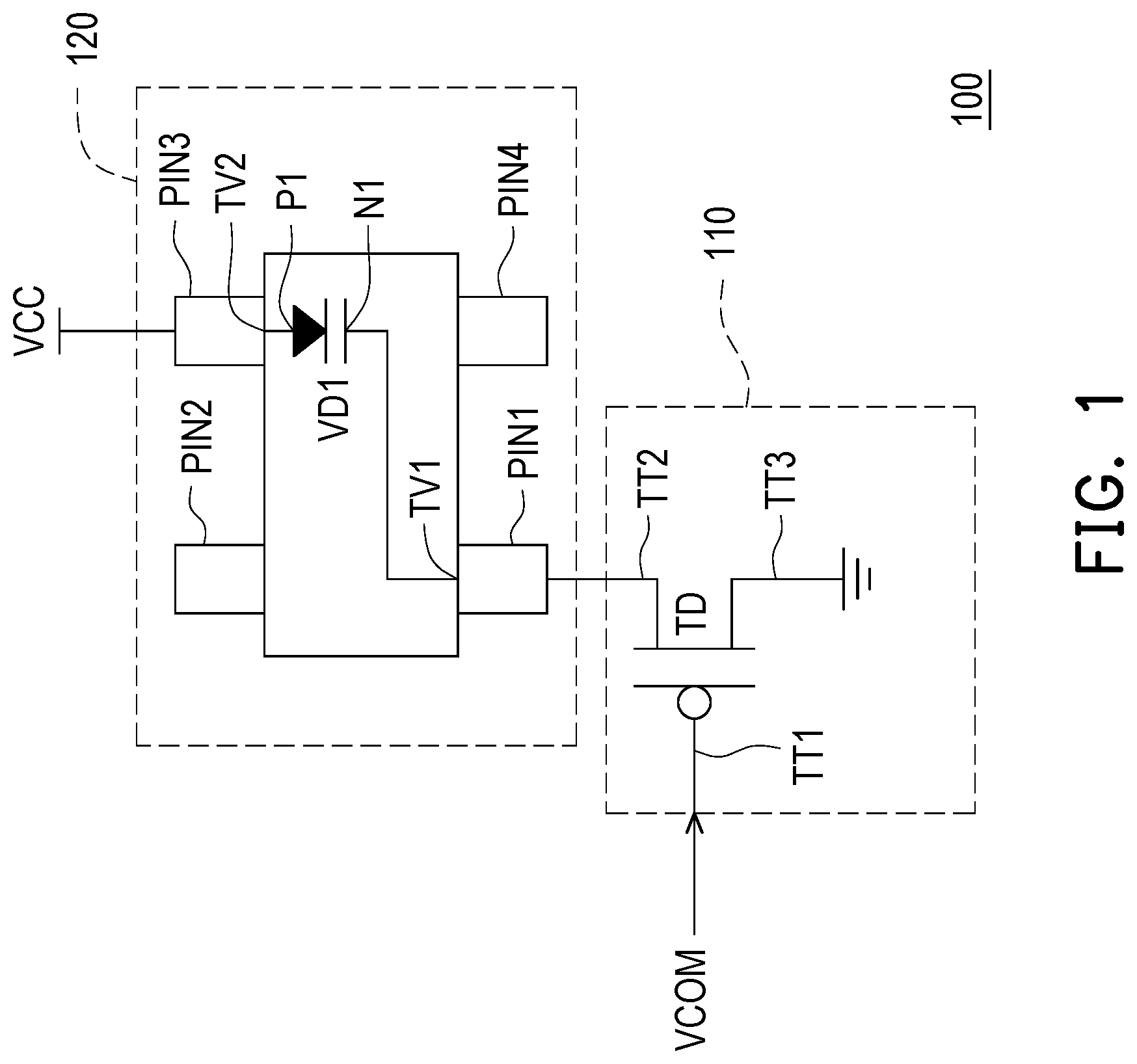
Please refer to , which is a schematic view of an electronic device according to an embodiment of the disclosure. In this embodiment, an electronic device 100 at least includes a switch circuit 110 and a diode 120 . The switch circuit 110 includes a transistor TD. The diode 120 has a first pin PIN 1 and a second pin PIN 2 . The first pin PIN 1 is electrically coupled to the transistor TD. The second pin PIN 2 is an idle contact.
In this embodiment, the transistor TD has a first terminal TT 1 , a second terminal TT 2 , and a third terminal TT 3 . In this exemplary embodiment, the transistor TD is a PMOS field effect transistor. The first terminal TT 1 of the transistor TD is a gate electrode. The second terminal TT 2 of the transistor TD is a source electrode. In addition, the third terminal TT 3 of the transistor TD is a drain electrode. The second terminal TT 2 of the transistor TD is electrically coupled to the first pin PIN 1 . The first terminal TT 1 of the transistor TD is coupled to a common voltage VCOM. In addition, the third terminal TT 3 of the transistor TD receives, for instance, a reference low voltage (e.g., grounded). An operating voltage VCC is greater than a voltage at the first terminal TT 1 (i.e., the gate electrode) of the transistor TD.
In this embodiment, the diode 120 further has a third pin PIN 3 and a fourth pin PIN 4 . In this exemplary embodiment, the third pin PIN 3 is electrically coupled to the operating voltage VCC. The fourth pin PIN 4 is an idle contact. In some embodiments, based on different designs, the electrical coupling manner of the first pin PIN 1 , the second pin PIN 2 , the third pin PIN 3 , and the fourth pin PIN 4 of the diode 120 may be different from the electrical coupling manner shown in . The electrical coupling manner provided in this disclosure is not limited to what is provided in the present embodiment.
In this embodiment, the switch circuit 110 may be a driver circuit or a compensation circuit adapted to the diode 120 , which should however not be construed as a limitation in the disclosure. The transistor TD is, for instance, a driving transistor configured to drive the diode 120 in the electronic device 100 , which should however not be construed as a limitation in the disclosure. The diode 120 is a polar element. In this embodiment, the diode 120 is, for instance, a varactor. In some embodiments, the diode 120 may be any type of the light emitting diode. In this embodiment, the electronic device 100 is, for instance, a frequency modulation device. In some embodiments, the electronic device 100 is, for instance, an antenna device.
In this embodiment, the diode 120 further has a first terminal TV 1 , a second terminal TV 2 , a first positive electrode P 1 , and a first negative electrode N 1 . The diode 120 includes a varactor element VD 1 . The first positive electrode P 1 is an anode of the varactor element VD 1 . The first negative electrode N 1 is a cathode of the varactor element VD 1 . The first negative electrode N 1 of the diode 120 is connected to the first terminal TV 1 . The first positive electrode P 1 of the diode 120 is connected to the second terminal TV 2 . In other words, the first negative electrode N 1 corresponds to the first pin PIN 1 . In this embodiment, the terminology “correspond to” means that different electrodes or pins are connected to the same side and at the same position. That is, the first negative electrode N 1 and the first pin PIN 1 are connected to the same side and at the same position. The first positive electrode P 1 corresponds to the third pin PIN 3 . That is, the first positive electrode P 1 and the third pin PIN 3 are connected to the same side and at the same position. Therefore, the first positive electrode P 1 of the diode 120 is coupled to the operating voltage VCC through the third pin PIN 3 . The first negative electrode N 1 of the diode 120 is coupled to the second terminal TT 2 of the transistor TD through the first pin PIN 1 (i.e., the source electrode). The diode 120 is applicable to the electronic device 100 and is compatible with a p-type transistor TD.
For further explanation, please refer to and at the same time. is a schematic view of a diode according to a first embodiment of the disclosure. In this embodiment, the first pin PIN 1 , the second pin PIN 2 , the third pin PIN 3 , and the fourth pin PIN 4 of the diode 120 are disposed in a point symmetrical manner. Further, the first pin PIN 1 , the second pin PIN 2 , the third pin PIN 3 , and the fourth pin PIN 4 are disposed in the point symmetrical manner with respect to the center of the diode 120 . Therefore, the position of the first pin PIN 1 before the diode 120 is rotated by 180° coincides with the position of the third pin PIN 3 after the diode 120 is rotated by 180°.
In this embodiment, the diode 120 further has a plurality of sides E 1 -E 4 . The first side E 1 and the second side E 2 are opposite to each other. The first pin PIN 1 and the fourth pin PIN 4 are disposed on the first side E 1 . The second pin PIN 2 and the third pin PIN 3 are disposed on the second side E 2 . The first pin PIN 1 and the third pin PIN 3 are disposed opposite to each other. In this embodiment, the fact that the first pin PIN 1 and the third pin PIN 3 are “disposed opposite to each other” means that the first pin PIN 1 and the third pin PIN 3 are respectively disposed on opposite sides, and the first pin PIN 1 and the third pin PIN 3 are the two pins with the longest distance therebetween in an extension direction DIR of the first side E 1 and the second side E 2 . Particularly, the first pin PIN 1 and the third pin PIN 3 are disposed in a point symmetrical manner, which means that after the first pin PIN 1 and the third pin PIN 3 are rotated by 180°, the first pin PIN 1 and the third pin PIN 3 coincide with their respective original positions. Based on different polarity designs, the transistor TD of the electronic device 100 may be an NMOS field effect transistor. The polarity of the diode 120 needs to be reversed. Therefore, it should be noted that the first pin PIN 1 and the third pin PIN 3 of the diode 120 are disposed in a point symmetrical manner according to the present embodiment, and thus the diode 120 is changed from a configuration CF 1 to a configuration CF 2 . The diode 120 provided in this embodiment may be rotated by 180° to complete the connection. In other words, the original third pin PIN 3 is replaced with the first pin PIN 1 . The original first pin PIN 1 is replaced with the third pin PIN 3 . As such, the rotation of the diode 120 may lead to an immediate reversion of the polarity of the diode 120 without changing the original layout position or layout space of the diode 120 .
The third side E 3 and the fourth side E 4 are opposite to each other. The first pin PIN 1 is spaced from the third side E 3 by a first distance DD 1 in the extension direction DIR of the first side E 1 . The third pin PIN 3 is spaced from the fourth side E 4 by the first distance DD 1 in the extension direction DIR of the second side E 2 . Therefore, the first pin PIN 1 and the third pin PIN 3 are disposed substantially in a diagonal manner across the diode 120 . In addition, the first side E 1 and the second side E 2 are parallel to each other. The third side E 3 and the fourth side E 4 are parallel to each other. Therefore, the first side E 1 and the second side E 2 have the same extension direction DIR.
The fourth pin PIN 4 is adjacent to the first pin PIN 1 . The second pin PIN 2 is adjacent to the third pin PIN 3 and opposite to the fourth pin PIN 4 . In this embodiment, the fact that the second pin PIN 2 and the fourth pin PIN 4 are “disposed opposite to each other” means that the second pin PIN 2 and the fourth pin PIN 4 are respectively disposed on opposite sides, and the second pin PIN 2 and the fourth pin PIN 4 are the two pins with the longest distance therebetween in the extension direction DIR. Specifically, the second pin PIN 2 is adjacent to the third pin PIN 3 along the extension direction DIR of the second side E 2 , which means that the distance between the second pin PIN 2 and the third pin PIN 3 in the extension direction DIR of the second side E 2 is relatively short as compared to other pins. The fourth pin PIN 4 is adjacent to the first pin PIN 1 along the extension direction DIR of the first side E 1 , which means that the distance between the fourth pin PIN 4 and the first pin PIN 1 in the extension direction DIR of the first side E 1 is relatively short as compared to other pins. The third pin PIN 3 is disposed on the second side E 2 . the fourth pin PIN 4 is disposed on the first side E 1 . The third pin PIN 3 and the fourth pin PIN 4 are disposed in a point symmetrical manner, which means that after the third pin PIN 3 and the fourth pin PIN 4 are rotated by 180°, the third pin PIN 3 and the fourth pin PIN 4 coincide with their respective original positions.
The second pin PIN 2 is spaced from the third side E 3 by a second distance DD 2 in the extension direction DIR of the second side E 2 . The fourth pin PIN 4 is spaced from the fourth side E 4 by the second distance DD 2 in the extension direction DIR of the first side E 1 . Therefore, the second pin PIN 2 and the fourth pin PIN 4 are disposed substantially in a diagonal manner across the diode 120 .
In this embodiment, the second distance DD 2 is substantially equal to the first distance DD 1 . In some embodiments, the second distance DD 2 is not equal to the first distance DD 1 .
At least one of the pins PIN 1 -PIN 4 is an idle contact. In this embodiment, the third pin PIN 3 and the fourth pin PIN 4 are idle contacts, respectively. That is, in this embodiment, the third pin PIN 3 and the fourth pin PIN 4 do not receive any signal or voltage.
For explanatory purposes, one single varactor device VD 1 and four pins PIN 1 -PIN 4 are taken as an example in this embodiment, which should however not be construed as a limitation in the disclosure. The number of the varactor elements in this disclosure may be one or plural. The number of the pins of the diode 120 in this disclosure may be plural or may be one or plural.
Please refer to and at the same time. is a schematic view of a diode according to a second embodiment of the disclosure. In this embodiment, the diode 220 has a plurality of pins PIN 1 -PIN 4 , a plurality of sides E 1 -E 4 , a first positive electrode P 1 , a second positive electrode P 2 , a first negative electrode N 1 , and a second negative electrode N 2 . In this embodiment, the point symmetrical manner in which the pins PIN 1 -PIN 4 are disposed on the sides E 1 -E 4 has been clearly explained in the embodiments depicted in and above and thus will not be further explained hereinafter.
In this embodiment, the first negative electrode N 1 corresponds to the first pin PIN 1 . The first positive electrode P 1 corresponds to the third pin PIN 3 . The second negative electrode N 2 corresponds to the fourth pin PIN 4 . The second positive electrode P 2 corresponds to the second pin PIN 2 . The first negative electrode N 1 is coupled to the first pin PIN 1 through the first terminal TV 1 . The first positive electrode P 1 is coupled to the third pin PIN 3 through the second terminal TV 2 . The second negative electrode N 2 is coupled to the fourth pin PIN 4 through the third terminal TV 3 . The second positive electrode P 2 is coupled to the second pin PIN 2 through the fourth terminal TV 4 .
The diode 120 includes varactor elements VD 1 , VD 2 , and VD 3 . The first positive electrode P 1 is the anode of the varactor elements VD 1 and VD 3 . The first negative electrode N 1 is the cathode of the varactor elements VD 1 and VD 2 . The second positive electrode P 2 is the anode of the varactor element VD 2 . The second negative electrode N 2 is the cathode of the varactor element VD 3 .
With reference to , at least one of the varactor elements VD 1 , VD 2 , and VD 3 is to be operated. For instance, in the configuration CF 1 , when the first pin PIN 1 is coupled to the operating voltage VCC, the second pin PIN 2 and the third pin PIN 3 are coupled to the second terminal TT 2 of the transistor TD, and the varactor elements VD 1 and VD 3 are operated. In the configuration CF 1 , the fourth pin PIN 2 is the idle contact. In the configuration CF 2 , the diode 220 provided in this embodiment may be rotated by 180° to complete the connection. Therefore, the first pin PIN 1 and the fourth pin PIN 4 are coupled to the second terminal TT 2 of the transistor TD, and the third pin PIN 3 is coupled to the operating voltage VCC. The varactor elements VD 1 and VD 3 are also operated. However, the polarity of the diode 220 is reversed without changing the original layout position or layout space of the diode 220 .
For instance, in the configuration CF 1 , when the first pin PIN 1 is coupled to the operating voltage VCC, the third pin PIN 3 is coupled to the second terminal TT 2 of the transistor TD, and the varactor element VD 1 is operated. In the configuration CF 2 , the diode 220 provided in this embodiment may be rotated by 180° to complete the connection. Therefore, when the first pin PIN 1 is coupled to the second terminal TT 2 of the transistor TD and the third pin PIN 3 is coupled to the operating voltage VCC, the varactor element VD 1 is also operated. In this embodiment, the second pin PIN 2 and the fourth pin PIN 4 are idle contacts, respectively.
For instance, in the configuration CF 1 , when the first pin PIN 1 and the fourth pin PIN 4 are coupled to the operating voltage VCC, the third pin PIN 3 is coupled to the second terminal TT 2 of the transistor TD, and the varactor elements VD 1 and VD 2 are operated. In the configuration CF 1 , the fourth pin PIN 4 is the idle contact. In the configuration CF 2 , the diode 220 provided in this embodiment may be rotated by 180° to complete the connection. Therefore, when the first pin PIN 1 is coupled to the second terminal TT 2 of the transistor TD and the second pin PIN 2 and third pin PIN 3 are coupled to the operating voltage VCC, the varactor elements VD 1 and VD 2 are also operated. In the configuration CF 2 , the second pin PIN 2 is the idle contact.
Please refer to and at the same time. is a schematic view of a diode according to a third embodiment of the disclosure. In this embodiment, a diode 320 has a plurality of pins PIN 1 -PIN 4 , a plurality of sides E 1 -E 4 , a first positive electrode P 1 , and a first negative electrode N 1 . In this embodiment, the point symmetrical manner in which the pins PIN 1 -PIN 4 are disposed on the sides E 1 -E 4 has been clearly explained in the embodiments depicted in and above and thus will not be further explained hereinafter.
In this embodiment, the first negative electrode N 1 corresponds to the first pin PIN 1 . The first positive electrode P 1 corresponds to the third pin PIN 3 . The first negative electrode N 1 is coupled to the first pin PIN 1 through the first terminal TV 1 . The first positive electrode P 1 is coupled to the third pin PIN 3 through the second terminal TV 2 . The diode 120 includes the varactor element VD 1 , a first capacitor C 1 , and a second capacitor C 2 . The first positive electrode P 1 is the anode of the varactor element VD 1 . The first negative electrode N 1 is the cathode of the varactor element VD 1 .
The first capacitor C 1 corresponds to the fourth pin PIN 4 . The second capacitor C 2 corresponds to the second pin PIN 2 . Specifically, the first capacitor C 1 is coupled between the third pin PIN 3 and the fourth pin PIN 4 . The second capacitor C 2 is coupled between the first pin PIN 1 and the second pin PIN 2 .
For instance, in the configuration CF 1 , when the first pin PIN 1 is coupled to the operating voltage VCC, the third pin PIN 3 is coupled to the second terminal TT 2 of the transistor TD, and the varactor element VD 1 is operated. In the configuration CF 2 , the diode 220 provided in this embodiment may be rotated by 180° to complete the connection. Therefore, when the first pin PIN 1 is coupled to the second terminal TT 2 of the transistor TD and the third pin PIN 3 is coupled to the operating voltage VCC, the varactor element VD 1 is also operated. In this embodiment, the second pin PIN 2 and the fourth pin PIN 4 are idle contacts, respectively.
For instance, in the configuration CF 1 , when the first pin PIN 1 and the fourth pin PIN 4 are coupled to the operating voltage VCC, the third pin PIN 3 is coupled to the second terminal TT 2 of the transistor TD, and the varactor element VD 1 and the second capacitor C 2 are operated. In the configuration CF 1 , the fourth pin PIN 4 is the idle contact. In the configuration CF 2 , the diode 320 provided in this embodiment may be rotated by 180° to complete the connection. Therefore, when the first pin PIN 1 is coupled to the second terminal TT 2 of the transistor TD and the second pin PIN 2 and the third pin PIN 3 are coupled to the operating voltage VCC, the varactor elements VD 1 and VD 2 are also operated. In the configuration CF 2 , the second pin PIN 2 is an idle contact.
Please refer to . is a circuit diagram of an electronic device according to an embodiment of the disclosure. In this embodiment, an electronic device 400 includes a switch circuit 410 , a diode 420 , and a selection circuit 430 . The switch circuit 410 includes transistors TB, TC, TD, and TR and a capacitor CC. The capacitor CC is coupled between a first terminal of the transistor TD and a common voltage VCOM. A second terminal of the transistor TD is coupled to a node NB. A first terminal of the transistor TR receives a reset signal RST. A second terminal of the transistor TR is coupled to the first terminal of the transistor TD. A third terminal of the transistor TR is coupled to a reference low voltage VSS. A first terminal of the transistor TC receives a selection signal SS. A second terminal of the transistor TC is coupled to the first terminal of the transistor TD. A third terminal of the transistor TC is coupled to a third terminal of the transistor TD. A first terminal of the transistor TB receives a bias voltage VB. A second terminal of the transistor TB is coupled to the third terminal of the transistor TD. A third terminal of the transistor TB is coupled to the reference low voltage VSS. In this embodiment, the switch circuit 410 is configured, for instance, to compensate a voltage value at the node NB.
The selection circuit 430 is coupled between a data line LD and the node NB. The selection circuit 430 provides a data voltage Vdata on the data line LD to the node NB in response to the selection signal SS. The selection circuit 430 includes a transistor TS. A first terminal of the transistor TS receives the selection signal SS. A second terminal of the transistor TS is coupled to the data line LD. A third terminal of the transistor TS is coupled to the node NB.
In this embodiment, the diode 420 is coupled between the operating voltage VCC and the node NB. The diode 420 may be, for instance, implemented in form of one of the diodes 120 , 220 , and 320 depicted in in to .
In this embodiment, the transistors TB, TC, TD, and TR are, for instance, implemented in form of the PMOS transistors. The transistor TS is, for instance, implemented in form of the NMOS transistor. Based on the description of the embodiments in to , it should be understood that if the transistors TB, TC, TD, and TR are respectively, for instance, implemented in form of the NMOS transistors instead, the diode 420 may be rotated by 180° to complete the connection. The rotation of the diode 420 may immediately reverse the polarity of the diode 420 without changing the original layout position or layout space of the diode 420 , and after the diode 420 is rotated by 180°, the operating voltage VCC connected to the second pin PIN 2 of the diode 720 should be greater than the voltage at the first terminal TT 1 of the transistor TD connected to the first pin PIN 1 . Similarly, the effect of polarity reversal in the PMOS transistors may also be achieved in the NMOS transistors.
To sum up, the diode provided in one or more embodiments of the disclosure is designed in a point symmetrical manner. As such, based on different polarity designs, the rotation of the diode may immediately reverse the polarity of the diode without changing the original layout position or layout space of the diode.
Although the embodiments of the disclosure and the advantages thereof have been disclosed above, it should be understood that any person skilled in the art can make changes, substitutions, and modifications without departing from the spirit and scope of the disclosure, and the features of the embodiments can be arbitrarily mixed and replaced to form other new embodiments. In addition, the protection scope of the disclosure is not limited to the process, machine, manufacture, material composition, device, method, and steps in the specific embodiments described in the specification. Any person skilled in the art can understand conventional or future-developed processes, machines, manufactures, material compositions, devices, methods, and steps from the content of the disclosure as long as the same can implement substantially the same functions or achieve substantially the same results in the embodiments described herein. Therefore, the protection scope of the disclosure includes the above processes, machines, manufactures, material compositions, devices, methods, and steps. In addition, each claim constitutes a separate embodiment, and the protection scope of the disclosure further includes combinations of the claims and the embodiments. The protection scope of the disclosure should be defined by the appended claims.
Figures (5)
Citations
This patent cites (2)
- US104467671
- US2007228231