Abstract
A semiconductor device, including a first gate, a second gate, a third gate, a first semiconductor layer, a second semiconductor layer, a source, and a drain, is provided. The first semiconductor layer is located between the first gate and the second gate. The second gate is located between the first semiconductor layer and the second semiconductor layer. The second semiconductor layer is located between the second gate and the third gate. The source is electrically connected to the first semiconductor layer and the second semiconductor layer. The drain is electrically connected to the first semiconductor layer and the second semiconductor layer.
Claims (13)
1. A semiconductor device, comprising: a first gate, a second gate, and a third gate; a first semiconductor layer and a second semiconductor layer, wherein the first semiconductor layer is located between the first gate and the second gate, the second gate is located between the first semiconductor layer and the second semiconductor layer, the second semiconductor layer is located between the second gate and the third gate, and the second semiconductor layer has a first through hole and a second through hole; a source, electrically connected to the first semiconductor layer and the second semiconductor layer, wherein the source passes through the first through hole to be electrically connected to the first semiconductor layer; and a drain, electrically connected to the first semiconductor layer and the second semiconductor layer, wherein the drain passes through the second through hole to be electrically connected to the first semiconductor layer.
12. A semiconductor device, comprising: a first gate, a second gate, and a third gate; a first semiconductor layer and a second semiconductor layer, wherein the first semiconductor layer is located between the first gate and the second gate, the second gate is located between the first semiconductor layer and the second semiconductor layer, and the second semiconductor layer is located between the second gate and the third gate; a source, electrically connected to the first semiconductor layer and the second semiconductor layer; a drain, electrically connected to the first semiconductor layer and the second semiconductor layer, wherein the source and the drain contact two opposite outer sidewalls of the second semiconductor layer; and an insulating structure, comprising: a first gate dielectric layer, located between the first gate and the first semiconductor layer; a second gate dielectric layer, located between the first semiconductor layer and the second gate; a third gate dielectric layer, located between the second gate and the second semiconductor layer, wherein a first contact hole and a second contact hole penetrate the second gate dielectric layer and the third gate dielectric layer, and the first contact hole and the second contact hole are located under the two opposite outer sidewalls of the second semiconductor layer; and a fourth gate dielectric layer, located between the second semiconductor layer and the third gate, wherein a third contact hole and a fourth contact hole penetrate the fourth gate dielectric layer, the third contact hole and the fourth contact hole respectively overlap with the first contact hole and the second contact hole, the source is filled into the first contact hole and the third contact hole to be electrically connected to the first semiconductor layer and the second semiconductor layer, the drain is filled into the second contact hole and the fourth contact hole to be electrically connected to the first semiconductor layer and the second semiconductor layer, and a width of the third contact hole and a width of the fourth contact hole are respectively greater than a width of the first contact hole and a width of the second contact hole.
Show 11 dependent claims
2. The semiconductor device according to claim 1 , further comprising: an insulating structure, covering the first gate, the second gate, the third gate, the first semiconductor layer, and the second semiconductor layer, wherein the insulating structure has a first contact hole, a second contact hole, a third contact hole, and a fourth contact hole, wherein the source and the drain are respectively filled into the first contact hole and the second contact hole to be electrically connected to the first semiconductor layer, and the source and the drain are respectively filled into the third contact hole and the fourth contact hole to be electrically connected to the second semiconductor layer.
3. The semiconductor device according to claim 1 , further comprising: a first gate dielectric layer, located between the first gate and the first semiconductor layer; a second gate dielectric layer, located between the first semiconductor layer and the second gate; a third gate dielectric layer, located between the second gate and the second semiconductor layer, wherein a first contact hole and a second contact hole penetrate the second gate dielectric layer and the third gate dielectric layer, the first contact hole and the second contact hole respectively overlap with the first through hole and the second through hole, and the source and the drain are respectively filled into the first contact hole and the second contact hole; and a fourth gate dielectric layer, located between the second semiconductor layer and the third gate, wherein a third contact hole and a fourth contact hole penetrate the fourth gate dielectric layer, the third contact hole and the fourth contact hole respectively overlap with the first through hole and the second through hole, and the source and the drain are respectively filled into the third contact hole and the fourth contact hole.
4. The semiconductor device according to claim 3 , wherein a width of the third contact hole and a width of the fourth contact hole are respectively greater than a width of the first through hole and a width of the second through hole.
5. The semiconductor device according to claim 3 , wherein the second semiconductor layer covers a part of a sidewall of the first contact hole and a part of a sidewall of the second contact hole.
6. The semiconductor device according to claim 5 , wherein the second semiconductor layer is located between the source and the third gate dielectric layer and between the drain and the third gate dielectric layer.
7. The semiconductor device according to claim 1 , wherein the first gate, the second gate, and the third gate are electrically connected to each other.
8. The semiconductor device according to claim 1 , wherein a length of the second semiconductor layer is less than a length of the first semiconductor layer.
9. The semiconductor device according to claim 1 , wherein the first semiconductor layer and the second semiconductor layer comprise a same material.
10. The semiconductor device according to claim 1 , wherein the first semiconductor layer and the second semiconductor layer comprise a same thickness.
11. The semiconductor device according to claim 1 , further comprising: a first gate dielectric layer, located between the first gate and the first semiconductor layer, wherein the first gate dielectric layer comprises a first nitride layer and a first oxygen-containing dielectric layer, wherein the first nitride layer contacts the first gate and the first oxygen-containing dielectric layer contacts the first semiconductor layer; a second gate dielectric layer, located between the first semiconductor layer and the second gate; a third gate dielectric layer, located between the second gate and the second semiconductor layer, wherein the third gate dielectric layer comprises a second nitride layer and a second oxygen-containing dielectric layer, wherein the second nitride layer contacts the second gate and the second oxygen-containing dielectric layer contacts the second semiconductor layer; and a fourth gate dielectric layer, located between the second semiconductor layer and the third gate.
13. The semiconductor device according to claim 12 , wherein the source and the drain contact the two opposite outer sidewalls and an upper surface of the second semiconductor layer.
Full Description
Show full text →
CROSS-REFERENCE TO RELATED APPLICATION
This application claims the priority benefit of U.S. Provisional Application No. 63/287,695, filed on Dec. 9, 2021 and Taiwan Application No. 111117305, filed on May 9, 2022. The entirety of each of the above-mentioned patent applications is hereby incorporated by reference herein and made a part of this specification.
BACKGROUND
Technical Field
The disclosure relates to a semiconductor device.
Description of Related Art
The dual-gate thin film transistor has the advantage of high driving current, so the dual-gate thin film transistor is often used as a driving element of an organic light emitting diode display device or a micro light emitting diode display device. Specifically, in order for the display device to have a sufficiently high resolution, the area of the driving element for driving a light emitting diode in the display device is limited. Therefore, many manufacturers choose to dispose the dual-gate thin film transistor as the driving element in the limited area, so that the driving element has a sufficiently high driving current.
However, compared with the conventional single-gate thin film transistor, the reliability of the dual-gate thin film transistor is lower, and the dual-gate thin film transistor is prone to driving current degradation and threshold voltage shift after long-term operation.
SUMMARY
The disclosure provides a semiconductor device, which can improve the negative influence caused by the current stress or the hot carrier effect.
A semiconductor device includes a first gate, a second gate, a third gate, a first semiconductor layer, a second semiconductor layer, a source, and a drain. The first semiconductor layer is located between the first gate and the second gate. The second gate is located between the first semiconductor layer and the second semiconductor layer. The second semiconductor layer is located between the second gate and the third gate. The source is electrically connected to the first semiconductor layer and the second semiconductor layer. The drain is electrically connected to the first semiconductor layer and the second semiconductor layer.
BRIEF DESCRIPTION OF THE DRAWINGS
A is a schematic top view of a semiconductor device according to an embodiment of the disclosure.
B is a schematic cross-sectional view taken along a line A-A′ of A .
C is a schematic cross-sectional view taken along a line B-B′ of A .
A to G are schematic cross-sectional views of a manufacturing method of the semiconductor device of A to C .
A is a schematic top view of a semiconductor device according to an embodiment of the disclosure.
B is a schematic cross-sectional view taken along a line A-A′ of A .
C is a schematic cross-sectional view taken along a line B-B′ of A .
A to E are schematic cross-sectional views of a manufacturing method of the semiconductor device of A to C .
A is a schematic top view of a semiconductor device according to an embodiment of the disclosure.
B is a schematic cross-sectional view taken along a line A-A′ of A .
C is a schematic cross-sectional view taken along a line B-B′ of A .
A to H are schematic cross-sectional views of a manufacturing method of the semiconductor device of A to C .
A is a schematic top view of a semiconductor device according to an embodiment of the disclosure.
B is a schematic cross-sectional view taken along a line A-A′ of A .
C is a schematic cross-sectional view taken along a line B-B′ of A .
is a schematic cross-sectional view of a manufacturing method of the semiconductor device of A to C .
is a schematic diagram of an equivalent circuit of a semiconductor device according to an embodiment of the disclosure.
DETAILED DESCRIPTION OF DISCLOSED EMBODIMENTS
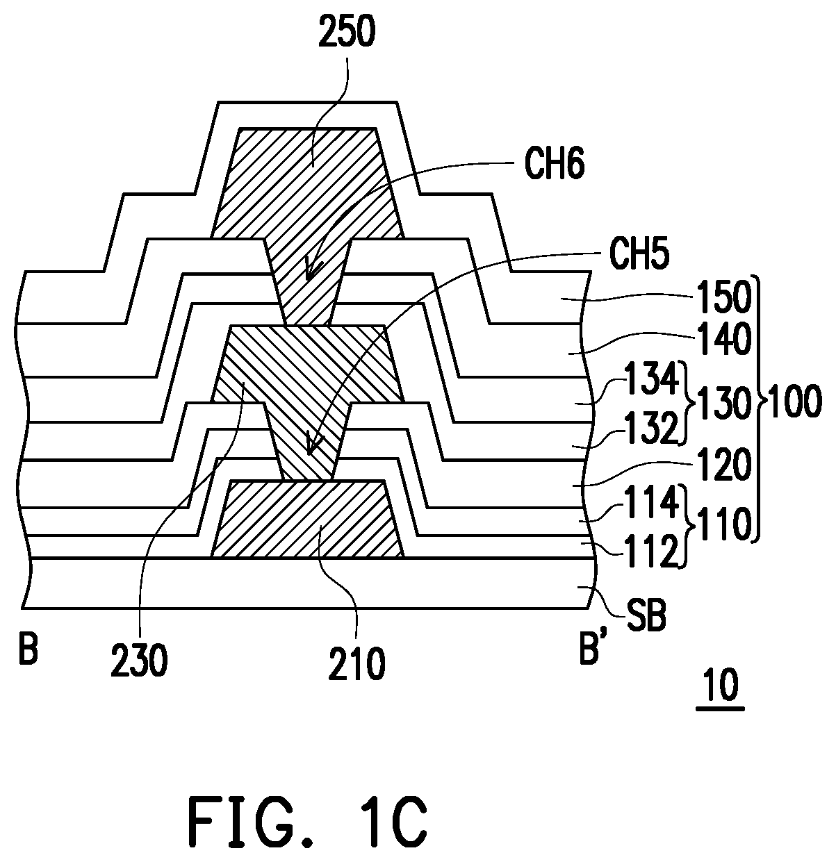
A is a schematic top view of a semiconductor device 10 according to an embodiment of the disclosure. B is a schematic cross-sectional view taken along a line A-A′ of A . C is a schematic cross-sectional view taken along a line B-B′ of A . In A , a first gate 210 , a second gate 230 , a third gate 250 , a first semiconductor layer 220 , a second semiconductor layer 240 , a source 262 , and a drain 264 are shown, and other components are omitted.
Please refer to A to C . The semiconductor device 10 includes the first gate 210 , the second gate 230 , the third gate 250 , the first semiconductor layer 220 , the second semiconductor layer 240 , the source 262 , and the drain 264 . In this embodiment, the semiconductor device 10 further includes a substrate SB and an insulating structure 100 .
The material of the substrate SB includes glass, quartz, organic polymer, opaque/reflective material (for example, conductive material, metal, wafer, ceramics, or other suitable materials), or other suitable materials. If the conductive material or the metal is used, an insulating layer (not shown) is covered on the substrate SB to avoid short circuit.
The first gate 210 , the second gate 230 , and the third gate 250 are located on the substrate 100 . In some embodiments, one or more buffer layers (not shown) are further included between the first gate 210 and the substrate 100 . The materials of the first gate 210 , the second gate 230 , and the third gate 250 include chromium, gold, silver, copper, tin, lead, hafnium, tungsten, molybdenum, neodymium, titanium, tantalum, aluminum, zinc, other metals, an alloy of the above, a metal oxide of the above, a metal nitride of the above, a combination of the above, or other conductive materials. For example, the first gate 210 , the second gate 230 , and the third gate 250 are each a stacked layer of titanium metal, aluminum metal, and titanium metal. The first gate 210 , the second gate 230 , and the third gate 250 are electrically connected to each other.
The first semiconductor layer 220 is located between the first gate 210 and the second gate 230 . The second gate 230 is located between the first semiconductor layer 220 and the second semiconductor layer 240 . The second semiconductor layer 240 is located between the second gate 220 and the third gate 250 .
The materials of the first semiconductor layer 220 and the second semiconductor layer 240 include amorphous silicon, polycrystalline silicon, microcrystalline silicon, monocrystalline silicon, organic semiconductor materials, metal oxide semiconductor materials (for example, indium gallium zinc oxide (IGZO), ZnO, SnO, indium zinc oxide (IZO), gallium zinc oxide (GZO), zinc tin oxide (ZTO), indium tin oxide (ITO), or other suitable materials), other suitable materials or a combination of the above materials. The material of the first semiconductor layer 220 and the material of the second semiconductor layer 240 are the same as or different from each other.
In some embodiments, the thickness of the first semiconductor layer 220 and the thickness of the second semiconductor layer 240 are 10 nm to 80 nm. The thickness of the first semiconductor layer 220 and the thickness of the second semiconductor layer 240 are the same as or different from each other.
In this embodiment, the first semiconductor layer 220 includes a first source region 222 , a first channel region 224 , and a first drain region 226 that are connected in sequence. The resistivities of the first source region 222 and the first drain region 226 are less than the resistivity of the first channel region 224 .
In this embodiment, the second semiconductor layer 240 includes a second source region 242 , a second channel region 244 , and a second drain region 246 that are connected in sequence. The resistivities of the second source region 242 and the second drain region 246 are less than the resistivity of the second channel region 244 .
In some embodiments, the first gate 210 , the second gate 230 , the third gate 250 , the first channel region 224 , and the second channel region 244 overlap in a normal direction ND of a top surface of the substrate SB. A length CL 1 of the first channel region 224 and a length CL 2 of the second channel region 244 are the same as or different from each other. In this embodiment, a length SL 2 of the second source region 242 and a length DL 2 of the second drain region 246 are less than a length SL 1 of the first source region 222 and a length DL 1 of the first drain region 226 , and the length of the second semiconductor layer 220 (the sum of the length SL 2 , the length CL 2 , and the length DL 2 ) is less than the length of the first semiconductor layer 220 (the sum of the length SL 1 , the length CL 1 , and the length DL 1 ).
The insulating structure 100 covers the first gate 210 , the second gate 230 , the third gate 250 , the first semiconductor layer 220 , and the second semiconductor layer 240 . The insulating structure 100 has a first contact hole CH 1 , a second contact hole CH 2 , a third contact hole CH 3 , and a fourth contact hole CH 4 . In this embodiment, the insulating structure 100 further includes a fifth contact hole CH 5 and a sixth contact hole CH 6 .
In this embodiment, the insulating structure 100 includes a first gate dielectric layer 110 , a second gate dielectric layer 120 , a third gate dielectric layer 130 , a fourth gate dielectric layer 140 , and a protective layer 150 .
The first gate dielectric layer 110 is located between the first gate 210 and the first semiconductor layer 220 . The first gate dielectric layer 110 has a single-layer or multi-layer structure. In this embodiment, the first gate dielectric layer 110 includes a first nitride layer 112 and a first oxygen-containing dielectric layer 114 . The first nitride layer 112 contacts the first gate 210 and the first oxygen-containing dielectric layer 114 contacts the first semiconductor layer 220 . In some embodiments, the material of the first nitride layer 112 includes, for example, silicon nitride or other suitable materials. In some embodiments, the thickness of the first nitride layer 112 is 30 nm to 300 nm. In some embodiments, the material of the first oxygen-containing dielectric layer 114 includes, for example, silicon oxynitride, silicon oxide, hafnium oxide, or other suitable materials. For example, the first oxygen-containing dielectric layer 114 is SiOxNy, where x is 1 to 0.5 and y is 0 to 0.5. In some embodiments, the thickness of the first oxygen-containing dielectric layer 114 is 50 nm to 200 nm.
The second gate dielectric layer 120 is located between the first semiconductor layer 220 and the second gate 230 . The second gate dielectric layer 120 has a single-layer or multi-layer structure. In this embodiment, the material of the second gate dielectric layer 120 includes, for example, silicon oxynitride, silicon oxide, hafnium oxide, or other suitable materials. In some embodiments, the thickness of the second gate dielectric layer 120 is 50 nm to 200 nm.
The third gate dielectric layer 130 is located between the second gate 230 and the second semiconductor layer 240 . The third gate dielectric layer 130 has a single-layer or multi-layer structure. In this embodiment, the third gate dielectric layer 130 includes a second nitride layer 132 and a second oxygen-containing dielectric layer 134 . The second nitride layer 132 contacts the second gate 230 and the second oxygen-containing dielectric layer 134 contacts the second semiconductor layer 240 . In some embodiments, the material of the second nitride layer 132 includes, for example, silicon nitride or other suitable materials. In some embodiments, the thickness of the second nitride layer 132 is 30 nm to 300 nm. In some embodiments, the material of the second oxygen-containing dielectric layer 134 includes, for example, silicon oxynitride, silicon oxide, hafnium oxide, or other suitable materials. For example, the second oxygen-containing dielectric layer 134 is SiOxNy, where x is 1 to 0.5 and y is 0 to 0.5. In some embodiments, the thickness of the second oxygen-containing dielectric layer 134 is 50 nm to 200 nm.
The fourth gate dielectric layer 140 is located between the second semiconductor layer 240 and the third gate 250 . The fourth gate dielectric layer 140 has a single-layer or multi-layer structure. In this embodiment, the material of the fourth gate dielectric layer 140 includes, for example, silicon oxynitride, silicon oxide, hafnium oxide, or other suitable materials. In some embodiments, the thickness of the fourth gate dielectric layer 140 is 50 nm to 200 nm.
The protective layer 150 covers the third gate 250 . The protective layer 150 has a single-layer or multi-layer structure. In this embodiment, the material of the protective layer 150 includes, for example, silicon oxynitride, silicon oxide, silicon nitride, or other suitable materials. In some embodiments, the thickness of the protective layer 150 is 100 nm to 600 nm.
In the insulating structure 100 , the first contact hole CH 1 and the second contact hole CH 2 penetrate the second gate dielectric layer 120 , the third gate dielectric layer 130 , the fourth gate dielectric layer 140 , and the protective layer 150 . The first contact hole CH 1 and the second contact hole CH 2 respectively overlap with the first source region 222 and the first drain region 226 of the first semiconductor layer 220 in the normal direction ND.
In the insulating structure 100 , the third contact hole CH 3 and the fourth contact hole CH 4 penetrate the fourth gate dielectric layer 140 and the protective layer 150 . The third contact hole CH 3 and the fourth contact hole CH 4 respectively overlap with the second source region 242 and the second drain region 246 of the second semiconductor layer 240 in the normal direction ND of the top surface of the substrate SB. The second semiconductor layer 240 is located between the first contact hole CH 1 and the second contact hole CH 2 , and the second semiconductor layer 240 is separated from the first contact hole CH 1 and the second contact hole CH 2 .
In the insulating structure 100 , the fifth contact hole CH 5 penetrates the first gate dielectric layer 110 and the second gate dielectric layer 120 , and the sixth contact hole CH 6 penetrates the third gate dielectric layer 130 and the fourth gate dielectric layer 140 . The second gate 230 is filled into the fifth contact hole CH 5 to be electrically connected to the first gate 210 , and the third gate 250 is filled into the sixth contact hole CH 6 to be electrically connected to the second gate 230 .
The source 262 and the drain 264 are respectively filled into the first contact hole CH 1 and the second contact hole CH 2 to be respectively electrically connected to the first source region 222 and the first drain region 226 of the first semiconductor layer 220 , and the source 262 and the drain 264 are respectively filled into the third contact hole CH 3 and the fourth contact hole CH 4 to be respectively electrically connected to the second source region 242 and the second drain region 246 of the second semiconductor layer 240 . The materials of the source 262 and the drain 264 include chromium, gold, silver, copper, tin, lead, hafnium, tungsten, molybdenum, neodymium, titanium, tantalum, aluminum, zinc, other metals, an alloy of the above, a metal oxide of the above, a metal nitride of the above, a combination of the above, or other conductive materials. For example, the source 262 and the drain 264 are each a stacked layer of titanium metal, aluminum metal, and titanium metal.
Based on the above, the semiconductor device 10 includes the first semiconductor layer 220 and the second semiconductor layer 240 , so as to disperse the current between the source 262 and the drain 264 , and improve the negative influence caused by the current stress or the hot carrier effect. In addition, the driving voltage of the semiconductor device 10 may be less than that of a dual-gate thin film transistor or a single-gate thin film transistor, so a preferred result can be obtained in a positive bias temperature stress (PBTS) test. The PBTS test is a test for measuring the amount of change in the threshold voltage under the condition of loading a positive voltage.
A to G are schematic cross-sectional views of a manufacturing method of the semiconductor device of A to C .
Please refer to A . The first gate 210 is formed on the substrate SB.
Please refer to B . The first gate dielectric layer 110 is formed on the first gate 210 . The method of forming the first gate dielectric layer 110 includes forming the first nitride layer 112 on the first gate 210 and forming the first oxygen-containing dielectric layer 114 on the first nitride layer 112 .
The first semiconductor material layer 220 ′ is formed on the first gate dielectric layer 110 .
Please refer to C . The second gate dielectric layer 120 is formed on the first material semiconductor layer 220 ′. The second gate 230 is formed on the second gate dielectric layer 120 . Using the second gate 230 as a mask, a doping process P 1 is executed on the first semiconductor material layer 220 ′ to form the first semiconductor layer 220 including the first source region 222 , the first channel region 224 , and the first drain region 226 , wherein the first channel region 224 is aligned with the second gate 230 . In some embodiments, the doping process P 1 includes a hydrogen plasma process, an ion implantation process, or other suitable processes. It should be noted that in some embodiments, hydrogen elements in the formed gate dielectric layer and the subsequently formed gate dielectric layer and/or protective layer may diffuse into the first semiconductor layer 220 during the process, thereby changing the hydrogen content in the first semiconductor layer 220 .
In some embodiments, before the second gate 230 is formed, an etching process is executed to form the fifth contact hole (please refer to C ) penetrating the first gate dielectric layer 110 and the second gate dielectric layer 120 , wherein the fifth contact hole exposes the first gate 210 . Next, the second gate 230 is formed in the fifth contact hole to be electrically connected to the first gate 210 .
Please refer to D . The third gate dielectric layer 130 is formed on the second gate 230 . The method of forming the third gate dielectric layer 130 includes forming the second nitride layer 132 on the second gate 230 and forming the second oxygen-containing dielectric layer 134 on the second nitride layer 132 .
A second material layer 240 ′ is formed on the third gate semiconductor dielectric layer 130 .
Please refer to E . The fourth gate dielectric layer 140 is formed on the second semiconductor material layer 240 ′.
The third gate 250 is formed on the fourth gate dielectric layer 140 . Using the third gate 250 as a mask, a doping process P 2 is executed on the second semiconductor material layer 240 ′ to form the second semiconductor layer 240 including the second source region 242 , the second channel region 244 , and the second drain region 246 , wherein the second channel region 244 is aligned with the third gate 250 . In some embodiments, the doping process P 2 includes a hydrogen plasma process, an ion implantation process, or other suitable processes. In some embodiments, hydrogen elements in the formed gate dielectric layer and the subsequently formed gate dielectric layer and/or protective layer may diffuse into the second semiconductor layer 240 during the process, thereby changing the hydrogen content in the second semiconductor layer 240 .
In some embodiments, before the third gate 250 is formed, an etching process is executed to form the sixth contact hole (please refer to C ) penetrating the third gate dielectric layer 130 and the fourth gate dielectric layer 140 , wherein the sixth contact hole exposes the second gate 230 . Next, the third gate 250 is formed in the sixth contact hole to be electrically connected to the second gate 230 .
Please refer to F . The protective layer 150 is formed on the third gate 250 . In some embodiments, the protective layer 150 contains hydrogen elements, and during the process of forming the protective layer 150 or after the protective layer 150 is formed, a heat treatment is performed to diffuse the hydrogen elements in the protective layer 150 downward to the second semiconductor layer 240 , thereby reducing the resistivity of the second semiconductor layer 240 .
Please refer to G . A patterning process is executed to form the insulating structure 100 having the first contact hole CH 1 , the second contact hole CH 2 , the third contact hole CH 3 , and the fourth contact hole CH 4 . The first contact hole CH 1 and the second contact hole CH 2 respectively expose the first source region 222 and the first drain region 226 of the first semiconductor layer 220 , and the third contact hole CH 3 and the fourth contact hole CH 4 respectively expose the second source region 242 and the second drain region 246 of the second semiconductor layer 240 . In some embodiments, the patterning process includes the following steps. A patterned photoresist layer (not shown) is formed on the protective layer 150 . Then, using the patterned photoresist layer as a mask, an etching process is executed on the protective layer 150 , the fourth gate dielectric layer 140 , the third gate dielectric layer 130 , and the second gate dielectric layer 120 . The first semiconductor layer 220 and the second semiconductor layer 240 may be used as etch stop layers for the etching process. In other words, the first contact hole CH 1 , the second contact hole CH 2 , the third contact hole CH 3 , and the fourth contact hole CH 4 may be formed together during the same etching process.
Finally, please return to B . The source 262 and the drain 264 are formed on the protective layer 150 , and the source 262 and the drain 264 are filled into the first contact hole CH 1 , the second contact hole CH 2 , the third contact hole CH 3 , and the fourth contact hole CH 4 . So far, the semiconductor device 10 is roughly completed.
A is a schematic top view of a semiconductor device 20 according to an embodiment of the disclosure. B is a schematic cross-sectional view taken along a line A-A′ of A . C is a schematic cross-sectional view taken along a line B-B′ of A . It must be noted here that the embodiment of A to C continue to use the reference numerals and some content of the embodiment of A to C , wherein the same or similar reference numerals are adopted to denote the same or similar elements, and the description of the same technical content is omitted. For the description of the omitted part, reference may be made to the foregoing embodiments, which will not be repeated here.
The main difference between the semiconductor device 20 of A to C and the semiconductor device 10 of A to C is that the second semiconductor layer 240 of the semiconductor device 20 has a first through hole TH 1 and a second through hole TH 2 .
Please refer to A to C . In this embodiment, the length SL 2 of the second source region 242 and the length DL 2 of the second drain region 246 are substantially equal to the length SL 1 of the first source region 222 and the length DL 1 of the first drain region 226 , and the length of the second semiconductor layer 220 (the sum of the length SL 2 , the length CL 2 , and the length DL 2 ) is substantially equal to the length of the first semiconductor layer 220 (the sum of the length SL 1 , the length CL 1 , and the length DL 1 ).
The first through hole TH 1 and the second through hole TH 2 are respectively located in the second source region 242 and the second drain region 246 of the second semiconductor layer 240 . The first through hole TH 1 and the second through hole TH 2 overlap with the first source region 222 and the first drain region 226 of the first semiconductor layer 220 in the normal direction ND of the top surface of the substrate SB.
The first contact hole CH 1 and the second contact hole CH 2 penetrate the second gate dielectric layer 120 and the third gate dielectric layer 130 . The first contact hole CH 1 and the second contact hole CH 2 respectively overlap with the first through hole TH 1 and the second through hole TH 2 in the normal direction ND of the top surface of the substrate SB.
The third contact hole CH 3 and the fourth contact hole CH 4 penetrate the fourth gate dielectric layer 140 and the protective layer 150 . The third contact hole CH 3 and the fourth contact hole CH 4 respectively overlap with the first through hole TH 1 and the second through hole TH 2 in the normal direction ND of the top surface of the substrate SB. The first through hole TH 1 is located between the first contact hole CH 1 and the third contact hole CH 3 , and the second through hole TH 2 is located between the second contact hole CH 2 and the fourth contact hole CH 4 .
The source 262 is filled into the first contact hole CH 1 , passes through the first through hole TH 1 , and is filled into the third contact hole CH 3 to be electrically connected to the first source region 222 of the first semiconductor layer 220 and the second source region 242 of the second semiconductor layer 240 . The drain 264 is filled into the second contact hole CH 2 , passes through the second through hole TH 2 , and is filled into the fourth contact hole CH 4 to be electrically connected to the first drain region 226 of the first semiconductor layer 220 and the second drain region 246 of the second semiconductor layer 240 .
In this embodiment, the width of the third contact hole CH 3 and the width of the fourth contact hole CH 4 are respectively greater than the width of the first through hole TH 1 and the width of the second through hole TH 2 . Therefore, the source 262 and the drain 264 not only contact a sidewall of the first through hole TH 1 and a sidewall of the second through hole TH 2 , but also contact a part of an upper surface of the second semiconductor layer 240 , so as to increase the contact area between the source 262 and the second semiconductor layer 240 and the contact area between the drain 264 and the second semiconductor layer 240 . In this embodiment, the contact area between the source 262 and the second semiconductor layer 240 is annular, and the contact area between the drain 264 and the second semiconductor layer 240 is also annular.
In this embodiment, the first contact hole CH 1 overlaps with the third contact hole CH 3 , so the distance between the source 262 and the first channel region 224 is approximately equal to the distance between the source 262 and the second channel region 244 . Similarly, the second contact hole CH 2 overlaps with the fourth contact hole CH 4 , so the distance between the drain 264 and the first channel region 224 is approximately equal to the distance between the drain 264 and the second channel region 244 . As such, current may be more evenly distributed to the first semiconductor layer 220 and the second semiconductor layer 240 .
Based on the above, the semiconductor device 20 includes the first semiconductor layer 220 and the second semiconductor layer 240 , so as to disperse the current between the source 262 and the drain 264 , and improve the negative influence caused by the current stress or the hot carrier effect. In addition, the driving voltage of the semiconductor device 20 may be less than the driving voltage of a dual-gate thin film transistor or a single-gate thin film transistor, so the semiconductor device 20 can obtain a preferred result in a PBTS test.
A to E are schematic cross-sectional views of a manufacturing method of the semiconductor device 20 of A to C .
Please refer to A . Following the steps of C , the third gate dielectric layer 130 is formed on the second gate 230 . The method of forming the third gate dielectric layer 130 includes forming the second nitride layer 132 on the second gate 230 and forming the second oxygen-containing dielectric layer 134 on the second nitride layer 132 .
The second material layer 240 ′ is formed on the third gate semiconductor dielectric layer 130 . In this embodiment, the second semiconductor material layer 240 ′ has the first through hole TH 1 and the second through hole TH 2 .
Please refer to B . The fourth gate dielectric layer 140 is formed on the second semiconductor material layer 240 ′. In this embodiment, the fourth gate dielectric layer 140 is filled into the first through hole TH 1 and the second through hole TH 2 .
The third gate 250 is formed on the fourth gate dielectric layer 140 . Using the third gate 250 as a mask, the doping process P 2 is executed on the second semiconductor material layer 240 ′ to form the second semiconductor layer 240 including the second source region 242 , the second channel region 244 , and the second drain region 246 , wherein the second channel region 244 is aligned with the third gate 250 . In some embodiments, the doping process P 2 includes a hydrogen plasma process, an ion implantation process, or other suitable processes. In some embodiments, hydrogen elements in the formed gate dielectric layer and the subsequently formed gate dielectric layer and/or protective layer may diffuse into the second semiconductor layer 240 during the process, thereby changing the hydrogen content in the second semiconductor layer 240 .
In some embodiments, before the third gate 250 is formed, an etching process is executed to form the sixth contact hole (please refer to C ) penetrating the third gate dielectric layer 130 and the fourth gate dielectric layer 140 , wherein the sixth contact hole exposes the second gate 230 . Next, the third gate 250 is formed in the sixth contact hole to be electrically connected to the second gate 230 .
Please refer to C . A patterned photoresist layer PR is formed on the protective layer 150 . The patterned photoresist layer PR includes a first opening OP 1 and a second opening OP 2 , wherein the first opening OP 1 and the second opening OP 2 respectively overlap with the first through hole TH 1 and the second through hole TH 2 in the normal direction ND of the top surface of the substrate SB. The width of the first opening OP 1 is greater than the width of the first through hole TH 1 , and the width of the second opening OP 2 is greater than the width of the second through hole TH 2 .
Please refer to D . Using the patterned photoresist layer PR as a mask, an etching process is executed on the protective layer 150 , the fourth gate dielectric layer 140 , the third gate dielectric layer 130 , and the second gate dielectric layer 120 . The first contact hole CH 1 , the second contact hole CH 2 , the third contact hole CH 3 , and the fourth contact hole CH 4 may be formed together during the same etching process. In this embodiment, since the width of the first opening OP 1 and the width of the second opening OP 2 are respectively greater than the width of the first through hole TH 1 and the width of the second through hole TH 2 , the third contact hole CH 3 and the fourth contact hole CH 4 expose on a part of the upper surface of the second semiconductor layer 240 . The second semiconductor layer 240 also serves as a mask of the etching process, so that the width of the first contact hole CH 1 and the width of the second contact hole CH 2 are respectively less than the width of the third contact hole CH 3 and the width of the fourth contact hole CH 4 . The first semiconductor layer 220 is an etch stop layer of the etching process.
Please refer to E . The patterned photoresist layer PR is removed.
Finally, please return to B . The source 262 and the drain 264 are formed on the protective layer 150 , and the source 262 and the drain 264 are filled into the first contact hole CH 1 , the second contact hole CH 2 , the third contact hole CH 3 , and the fourth contact hole CH 4 . So far, the semiconductor device 20 is roughly completed.
A is a schematic top view of a semiconductor device 30 according to an embodiment of the disclosure. B is a schematic cross-sectional view taken along a line A-A′ of A . C is a schematic cross-sectional view taken along a line B-B′ of A . It must be noted here that the embodiment of A to C continue to use the reference numerals and some content of the embodiment of A to C , the same or similar reference numerals are adopted to denote the same or similar elements, and the description of the same technical content is omitted. For the description of the omitted part, reference may be made to the foregoing embodiments, which will not be repeated here.
The main difference between the semiconductor device 30 of A to C and the semiconductor device 20 of A to C is that the second semiconductor layer 240 of the semiconductor device 30 covers a part of a sidewall of the first contact hole CH 1 and a part of a sidewall of the second contact hole CH 2 .
Please refer to A to C . A part of the second semiconductor layer 240 extends toward the substrate SB along the sidewall of the first contact hole CH 1 at the first contact hole CH 1 , and a part of the second semiconductor layer 240 extends toward the substrate SB along the sidewall of the second contact hole CH 2 at the second contact hole CH 2 . The second semiconductor layer 240 is located between the source 262 and the third gate dielectric layer 130 and between the drain 264 and the third gate dielectric layer 130 . In this embodiment, the second semiconductor layer 240 does not extend beyond a bottom surface of the third gate dielectric layer 130 , but the disclosure is not limited thereto. In some embodiments, the second semiconductor layer 240 extends beyond the bottom surface of the third gate dielectric layer 130 , but the second semiconductor layer 240 does not pass through the second gate dielectric layer 120 .
In this embodiment, by adjusting the contact area between the source 262 and the first semiconductor layer 220 , the contact area between the drain 264 and the first semiconductor layer 220 , the contact area between the source 262 and the second semiconductor layer 240 , and the contact area between the drain 264 and the second semiconductor layer 240 , current may be more evenly distributed to the first semiconductor layer 220 and the second semiconductor layer 240 .
In this embodiment, the first contact hole CH 1 overlaps with the third contact hole CH 3 , so the distance between the source 262 and the first channel region 224 is approximately equal to the distance between the source 262 and the second channel region 244 . Similarly, the second contact hole CH 2 overlaps with the fourth contact hole CH 4 , so the distance between the drain 264 and the first channel region 224 is approximately equal to the distance between the drain 264 and the second channel region 244 . As such, current may be more evenly distributed to the first semiconductor layer 220 and the second semiconductor layer 240 .
Based on the above, the semiconductor device 30 includes the first semiconductor layer 220 and the second semiconductor layer 240 , so as to disperse the current between the source 262 and the drain 264 , and improve the negative influence caused by the current stress or the hot carrier effect. In addition, the driving voltage of the semiconductor device 30 may be less than the driving voltage of a dual-gate thin film transistor or a single-gate thin film transistor, so the semiconductor device 30 can obtain a preferred result in a PBTS test.
A to H are schematic cross-sectional views of a manufacturing method of the semiconductor device 30 of A to C .
Please refer to A . Following the steps of C , the third gate dielectric layer 130 is formed on the second gate 230 . The method of forming the third gate dielectric layer 130 includes forming the second nitride layer 132 on the second gate 230 and forming the second oxygen-containing dielectric layer 134 on the second nitride layer 132 .
Please refer to B . An etching process is executed to form a first opening CH 1 ′ and a second opening CH 2 ′ penetrating the third gate dielectric layer 130 . In this embodiment, the first opening CH 1 ′ and the second opening CH 2 ′ do not penetrate the second gate dielectric layer 120 . In this embodiment, the etching process is stopped at the second gate dielectric layer 120 .
Please refer to C . The second semiconductor material layer 240 ′ is formed on the third gate dielectric layer 130 . The second semiconductor material layer 240 ′ is filled into the first opening CHF and the second opening CH 2 ′, and contacts the second gate dielectric layer 120 . The second semiconductor material layer 240 ′ has the first through hole TH 1 and the second through hole TH 2 . The first through hole TH 1 exposes a part of the second gate dielectric layer 120 at the bottom of the first opening CH 1 ′. The second through hole TH 2 exposes a part of the second gate dielectric layer 120 at the bottom of the second opening CH 2 ′.
Please refer to D . The fourth gate dielectric layer 140 is formed on the second semiconductor material layer 240 ′. The fourth gate dielectric layer 140 is filled into the first opening CH 1 ′ and the second opening CH 2 ′, and contacts the second gate dielectric layer 120 .
The third gate 250 is formed on the fourth gate dielectric layer 140 . Using the third gate 250 as a mask, the doping process P 2 is executed on the second semiconductor material layer 240 ′ to form the second semiconductor layer 240 including the second source region 242 , the second channel region 244 , and the second drain region 246 , wherein the second channel region 244 is aligned with the third gate 250 . In some embodiments, the doping process P 2 includes a hydrogen plasma process, an ion implantation process, or other suitable processes. In some embodiments, hydrogen elements in the formed gate dielectric layer and the subsequently formed gate dielectric layer and/or protective layer may diffuse into the second semiconductor layer 240 during the process, thereby changing the hydrogen content in the second semiconductor layer 240 .
In some embodiments, before the third gate 250 is formed, an etching process is executed to form the sixth contact hole (please refer to C ) penetrating the third gate dielectric layer 130 and the fourth gate dielectric layer 140 , wherein the sixth contact hole exposes the second gate 230 . Next, the third gate 250 is formed in the sixth contact hole to be electrically connected to the second gate 230 .
Please refer to E . The protective layer 150 is formed on the third gate 250 .
Please refer to F . The patterned photoresist layer PR is formed on the protective layer 150 . The patterned photoresist layer PR includes the first opening OP 1 and the second opening OP 2 , wherein the first opening OP 1 and the second opening OP 2 respectively overlap with the first through hole TH 1 and the second through hole TH 2 in the normal direction ND of the top surface of the substrate SB. The width of the first opening OP 1 is greater than the width of the first through hole TH 1 , and the width of the second opening OP 2 is greater than the width of the second through hole TH 2 .
Please refer to G . Using the patterned photoresist layer PR as a mask, an etching process is executed on the protective layer 150 , the fourth gate dielectric layer 140 , the third gate dielectric layer 130 , and the second gate dielectric layer 120 . The first contact hole CH 1 , the second contact hole CH 2 , the third contact hole CH 3 , and the fourth contact hole CH 4 may be formed together during the same etching process. In this embodiment, since the width of the first opening OP 1 and the width of the second opening OP 2 are respectively greater than the width of the first through hole TH 1 and the width of the second through hole TH 2 , the third contact hole CH 3 and the fourth contact hole CH 4 expose a part of the upper surface of the second semiconductor layer 240 . The second semiconductor layer 240 also serves as a mask of the etching process, so that the width of the first contact hole CH 1 and the width of the second contact hole CH 2 are respectively less than the width of the third contact hole CH 3 and the width of the fourth contact hole CH 4 . The first semiconductor layer 220 is an etch stop layer of the etching process.
Please refer to H . The patterned photoresist layer PR is removed.
Finally, please return to B . The source 262 and the drain 264 are formed on the protective layer 150 , and the source 262 and the drain 264 are filled into the first contact hole CH 1 , the second contact hole CH 2 , the third contact hole CH 3 , and the fourth contact hole CH 4 . So far, the semiconductor device 30 is roughly completed.
A is a schematic top view of a semiconductor device 40 according to an embodiment of the disclosure. B is a schematic cross-sectional view taken along a line A-A′ of A . C is a schematic cross-sectional view taken along a line B-B′ of A . It must be noted here that the embodiment of A to C continue to use the reference numerals and some content of the embodiment of A to C , wherein the same or similar reference numerals are adopted to denote the same or similar elements, and the description of the same technical content is omitted. For the description of the omitted part, reference may be made to the foregoing embodiments, which will not be repeated here.
The main difference between the semiconductor device 40 of A to C and the semiconductor device 10 of A to C is that the source 262 and the drain 264 of the semiconductor device 40 contact two opposite outer sidewalls of the second semiconductor layer 240 .
Please refer to A to C . The first contact hole CH 1 and the second contact hole CH 2 penetrate the second gate dielectric layer 120 and the third gate dielectric layer 130 . The first contact hole CH 1 and the second contact hole CH 2 are located under the two opposite outer sidewalls of the second semiconductor layer 240 . The third contact hole CH 3 and the fourth contact hole CH 4 penetrate the fourth gate dielectric layer 140 and the protective layer 150 . The third contact hole CH 3 and the fourth contact hole CH 4 respectively overlap with the first contact hole CH 1 and the second contact hole CH 2 . The width of the third contact hole CH 3 and the width of the fourth contact hole CH 4 are respectively greater than the width of the first contact hole CH 1 and the width of the second contact hole CH 2 .
The source 262 is filled into the first contact hole CH 1 and the third contact hole CH 3 to be electrically connected to the first source region 222 of the first semiconductor layer 220 and the second source region 242 of the second semiconductor layer 240 . The drain 264 is filled into the second contact hole CH 2 and the fourth contact hole CH 4 to be electrically connected to the first drain region 226 of the first semiconductor layer 220 and the second drain region 246 of the second semiconductor layer 240 . The source 262 and the drain 264 contact the two opposite outer sidewalls and the upper surface of the second semiconductor layer 240 .
In this embodiment, the first contact hole CH 1 overlaps with the third contact hole CH 3 , so the distance between the source 262 and the first channel region 224 is approximately equal to the distance between the source 262 and the second channel region 244 . Similarly, the second contact hole CH 2 overlaps with the fourth contact hole CH 4 , so the distance between the drain 264 and the first channel region 224 is approximately equal to the distance between the drain 264 and the second channel region 244 . As such, current may be more evenly distributed to the first semiconductor layer 220 and the second semiconductor layer 240 .
Based on the above, the semiconductor device 40 includes the first semiconductor layer 220 and the second semiconductor layer 240 , so as to disperse the current between the source 262 and the drain 264 , and improve the negative influence caused by the current stress or the hot carrier effect. In addition, the driving voltage of the semiconductor device 40 may be less than the driving voltage of a dual-gate thin film transistor or a single-gate thin film transistor, so the semiconductor device 40 can obtain a preferred result in a PBTS test.
is a schematic cross-sectional view of a manufacturing method of the semiconductor device 40 of A to C .
Please refer to . Following the steps of F , a patterning process is executed to form the insulating structure 100 having the first contact hole CH 1 , the second contact hole CH 2 , the third contact hole CH 3 , and the fourth contact hole CH 4 . The first contact hole CH 1 and the second contact hole CH 2 respectively expose the first source region 222 and the first drain region 226 of the first semiconductor layer 220 , and the third contact hole CH 3 and the fourth contact hole CH 4 respectively expose the second source region 242 and the second drain region 246 of the second semiconductor layer 240 . In some embodiments, the patterning process includes the following steps. A patterned photoresist layer (not shown) is formed on the protective layer 150 . Then, using the patterned photoresist layer as a mask, an etching process is executed on the protective layer 150 , the fourth gate dielectric layer 140 , the third gate dielectric layer 130 , and the second gate dielectric layer 120 . The second semiconductor layer 240 may serve as a mask of the etching process, and the first semiconductor layer 220 may serve as an etch stop layer of the etching process. In other words, the first contact hole CH 1 , the second contact hole CH 2 , the third contact hole CH 3 , and the fourth contact hole CH 4 may be formed together during the same etching process.
Finally, please return to B . The source 262 and the drain 264 are formed on the protective layer 150 , and the source 262 and the drain 264 are filled into the first contact hole CH 1 , the second contact hole CH 2 , the third contact hole CH 3 , and the fourth contact hole CH 4 . So far, the semiconductor device 40 is roughly completed.
is a schematic diagram of an equivalent circuit of a semiconductor device according to an embodiment of the disclosure. For example, is, for example, a schematic diagram of an equivalent circuit of the semiconductor device 10 of A to C , the semiconductor device 20 of A to C , the semiconductor device 30 of A to C , or the semiconductor device 40 of A to C .
Please refer to . The equivalent circuit of the semiconductor device is substantially equal to two switching elements TFT 1 and TFT 2 connected together. The switching element TFT 1 includes a gate G 1 , the switching element TFT 2 includes a gate G 3 , and the switching element TFT 1 and the switching element TFT 2 share a gate G 2 . The switching element TFT 1 and the switching element TFT 2 share a source S, and the switching element TFT 1 and the switching element TFT 2 share a drain D. Current is distributed to a channel (for example, the first semiconductor layer) of the switching element TFT 1 and a channel (for example, the second semiconductor layer) of the switching element TFT 2 , so the negative influence caused by the current stress or the hot carrier effect can be improved.
Figures (3)
Citations
This patent cites (18)
- US5909615
- US7265393
- US9601518
- US9653493
- US2004/0174349
- US2007/0272948
- US2009/0020817
- US2010/0044708
- US2013/0161713
- US2020/0411511
- US110429139
- US111223939
- US113113425
- US2003273228
- US2017011173
- US2017011173
- USI302032
- US201009954