Radio Frequency Module and Communication Device
Abstract
A radio frequency module and a communication device capable of further suppressing a decrease in reception sensitivity are provided. A radio frequency module includes a switch (second switch), a reception filter (second reception filter), a low-noise amplifier (second low-noise amplifier), and a filter (second filter). The switch is configured to change over between a transmission path of a transmission signal and a reception path of a reception signal in communication based on a time division duplex system. The reception filter is provided at a subsequent stage of the switch and is configured to pass the reception signal in a predetermined frequency band. The low-noise amplifier is configured to amplify the reception signal that has passed through the reception filter. The filter is provided at a preceding stage of the switch in the reception path (second reception path).
Claims (15)
1. A radio frequency module, comprising: a switch configured to selectively change between a transmission path of a transmission signal and a reception path of a reception signal in communication based on a time division duplex system; a reception filter at a stage subsequent to the switch, the reception filter being configured to pass the reception signal in a predetermined frequency band; a low-noise amplifier configured to amplify the reception signal that has passed through the reception filter; and a filter between an antenna terminal and the switch, at a stage preceding the switch in the reception path, wherein the filter is configured to attenuate a signal in a second frequency band, the second frequency band being lower than the predetermined frequency band.
8. A radio frequency module, comprising: a switch configured to selectively change a connection destination of an antenna terminal; a transmission/reception filter at a stage subsequent to the switch, the transmission/reception filter being configured to pass a reception signal in a predetermined frequency band and to pass a transmission signal in the predetermined frequency band; a low-noise amplifier configured to amplify the reception signal that has passed through the transmission/reception filter; and a filter between the antenna terminal and the switch, at a stage preceding the switch in a reception path of the reception signal, wherein the filter is configured to attenuate a signal in a second frequency band, the second frequency band being lower than the predetermined frequency band.
15. A radio frequency module, comprising: a switch configured to selectively change between a transmission path of a transmission signal and a reception path of a reception signal in communication based on a time division duplex system; a reception filter at a stage subsequent to the switch, the reception filter being configured to pass the reception signal in a predetermined frequency band; a low-noise amplifier configured to amplify the reception signal that has passed through the reception filter; and a plurality of sets of: a filter between an antenna terminal and the switch, at a stage preceding the switch in the reception path; and a changeover switch configured to selectively connect and disconnect the filter to the reception path, wherein the plurality of filters of the plurality of sets have different attenuation bands.
Show 12 dependent claims
2. The radio frequency module according to claim 1 , further comprising: a changeover switch configured to selectively connect and disconnect the filter to the reception path.
3. The radio frequency module according to claim 1 , wherein an attenuation band of the filter is variable.
4. The radio frequency module according to claim 2 , comprising a plurality of sets of the filter and the changeover switch, wherein the plurality of filters of the plurality of sets have different attenuation bands.
5. The radio frequency module according to claim 1 , wherein the second frequency band comprises a frequency that is half of a frequency of the reception signal.
6. The radio frequency module according to claim 1 , wherein the filter is a notch filter or a high pass filter.
7. A communication device, comprising: the radio frequency module according to claim 1 ; and a signal processing circuit configured to process a signal passing through the radio frequency module.
9. The radio frequency module according to claim 8 , further comprising: a changeover switch configured to selectively connect and disconnect the filter to the reception path.
10. The radio frequency module according to claim 8 , wherein an attenuation band of the filter is variable.
11. The radio frequency module according to claim 9 , comprising a plurality of sets of the filter and the changeover switch, wherein the plurality of filters of the plurality of sets have different attenuation bands.
12. The radio frequency module according to claim 8 , wherein the second frequency band comprises a frequency that is half of a frequency of the reception signal.
13. The radio frequency module according to claim 8 , wherein the filter is a notch filter or a high pass filter.
14. A communication device, comprising: the radio frequency module according to claim 8 ; and a signal processing circuit configured to process a signal passing through the radio frequency module.
Full Description
Show full text →
CROSS REFERENCE TO RELATED APPLICATION
This is a continuation of International Application No. PCT/JP2021/019444 filed on May 21, 2021 which claims priority from Japanese Patent Application No. 2020-102570 filed on Jun. 12, 2020. The contents of these applications are incorporated herein by reference in their entireties.
BACKGROUND ART
Technical Field
The present disclosure generally relates to a radio frequency module and a communication device, and more particularly to a radio frequency module and a communication device that communicate based on a time division duplex system.
A radio frequency front-end circuit (radio frequency module) capable of suppressing a decrease in reception sensitivity has been known (see Patent Document 1).
The radio frequency front-end circuit of Patent Document 1 includes a transmission circuit and a reception circuit, and transmits and receives at the same time. The transmission circuit includes a transmission filter to pass a signal in a transmission frequency band, and the reception circuit includes a reception filter to pass a signal in a reception frequency band different from the transmission frequency band, a low-noise amplifier that inputs and amplifies a signal outputted from the reception filter, and a filter circuit connected between the reception filter and the low-noise amplifier. The filter circuit attenuates a signal of a frequency indicating a difference between a center frequency of a transmission frequency band and a center frequency of a reception frequency band among signals inputted to the low-noise amplifier.
•
• Patent Document 1: Japanese Unexamined Patent Application Publication No. 2019-29700
BRIEF SUMMARY
In a configuration of a radio frequency front-end circuit (radio frequency module), there is a case that a switch for changing over a path of a signal is provided at a preceding stage of a reception filter or a transmission/reception filter to pass a reception signal in a predetermined frequency band. In the case above, a harmonic wave of a signal in a band lower than the reception frequency band is generated because of nonlinear characteristics of the switch. Accordingly, when a signal in the reception frequency band passes through the reception filter, there is a possibility that reception sensitivity decreases. In the radio frequency front-end circuit (radio frequency module) of Patent Document 1, a harmonic wave generated by switching of a switch cannot be removed. In the case above, in the radio frequency front-end circuit (radio frequency module) of Patent Document 1, reception sensitivity decreases.
The present disclosure provides a radio frequency module and a communication device capable of further suppressing a decrease in reception sensitivity.
A radio frequency module according to an aspect of the present disclosure includes a switch, a reception filter, a low-noise amplifier, and a filter. The switch is configured to change over between a transmission path of a transmission signal and a reception path of a reception signal in communication based on a time division duplex system. The reception filter is provided at a subsequent stage of the switch and is configured to pass the reception signal in a predetermined frequency band. The low-noise amplifier is configured to amplify the reception signal that has passed through the reception filter. The filter is provided at a preceding stage of the switch in the reception path.
A radio frequency module according to an aspect of the present disclosure includes a switch, a transmission/reception filter, a low-noise amplifier, and a filter. The switch is configured to change over a connection destination of an antenna terminal. The transmission/reception filter is provided at a subsequent stage of the switch and is configured to pass a reception signal in a predetermined frequency band and a transmission signal in the predetermined frequency band. The low-noise amplifier is configured to amplify the reception signal that has passed through the transmission/reception filter. The filter is provided at a preceding stage of the switch in a reception path of the reception signal.
A communication device according to an aspect of the present disclosure includes the radio frequency module and a signal processing circuit configured to process a signal passing through the radio frequency module.
According to the present disclosure, a decrease in reception sensitivity may further be suppressed.
BRIEF DESCRIPTION OF THE DRAWINGS
is a circuit diagram for explaining a circuit configuration of a radio frequency module and a communication device according to Embodiment 1.
is a diagram for explaining an operation example of the radio frequency module above during operation.
A is a diagram for explaining a circuit configuration of a radio frequency module according to Modification 1 of Embodiment 1. B is a diagram for explaining a circuit configuration of a radio frequency module according to Modification 2 of Embodiment 1.
A is a diagram for explaining a circuit configuration of a radio frequency module according to Modification 3 of Embodiment 1. B is a diagram for explaining a circuit configuration of a radio frequency module according to Modification 4 of Embodiment 1.
is a diagram for explaining a circuit configuration of a radio frequency module and a communication device according to Modification 5 of Embodiment 1.
is a diagram for explaining a circuit configuration of a radio frequency module and a communication device according to Modification 6 of Embodiment 1.
is a diagram for explaining a circuit configuration of a radio frequency module and a communication device according to Modification 7 of Embodiment 1.
is a circuit diagram for explaining a circuit configuration of a radio frequency module and a communication device according to Embodiment 2.
A is a diagram for explaining a circuit configuration of a radio frequency module according to Modification 1 of Embodiment 2. B is a diagram for explaining a circuit configuration of a radio frequency module according to Modification 2 of Embodiment 2.
is a diagram for explaining a circuit configuration of a radio frequency module according to Modification 3 of Embodiment 2.
is a diagram for explaining a circuit configuration of a radio frequency module according to Modification 4 of Embodiment 2.
DETAILED DESCRIPTION
to referred to in the following embodiments or the like are all schematic views, and ratios of sizes and thicknesses of constituents in the drawings do not necessarily reflect actual dimensional ratios.
Embodiment 1
Hereinafter, a radio frequency module 1 and a communication device 10 including the radio frequency module 1 according to Embodiment 1 will be described with reference to to .
(1) Radio Frequency Module
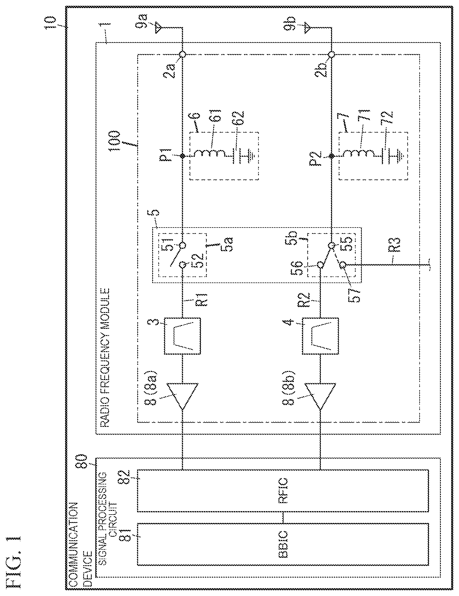
The radio frequency module 1 according to Embodiment 1 includes a reception module 100 as illustrated in . The radio frequency module 1 further includes a transmission module (not illustrated).
The radio frequency module 1 (reception module 100 thereof) includes a first antenna terminal 2 a , a second antenna terminal 2 b , a first reception filter 3 , a second reception filter 4 (reception filter), a switch 5 , a first filter 6 , and a second filter 7 (filter). The radio frequency module 1 (reception module 100 thereof) includes a first low-noise amplifier 8 a and a second low-noise amplifier 8 b as amplifiers 8 to amplify signals.
The radio frequency module 1 is a module capable of supporting carrier aggregation (Carrier Aggregation) and dual connectivity (Dual Connectivity). In Embodiment 1, the radio frequency module 1 supports simultaneous use of a time division duplex (TDD) signal and a frequency division duplex (FDD) signal. Here, Carrier Aggregation and Dual Connectivity refer to communication that simultaneously uses radio waves of multiple frequency bands. Hereinafter, communication by Carrier Aggregation or Dual Connectivity is also referred to as simultaneous communication.
The radio frequency module 1 is used in a mobile phone such as a smartphone, for example. Note that the radio frequency module 1 may be used in a wearable terminal such as a smart watch, for example, not limited in a mobile phone. In short, the radio frequency module 1 is used in the communication device 10 to communicate with an external device (not illustrated) as illustrated in .
(2) Constituents of Radio Frequency Module
Hereinafter, constituents of the radio frequency module 1 according to Embodiment 1 will be described with reference to the drawings.
The first antenna terminal 2 a is electrically connected to an antenna 9 a as illustrated in . The second antenna terminal 2 b is electrically connected to an antenna 9 b as illustrated in .
The first reception filter 3 is provided in a first reception path R 1 for receiving a first reception signal in a first communication band used in FDD communication from the antenna 9 b by FDD, as illustrated in . Here, the first reception path R 1 is a path for receiving a first reception signal by FDD through the first antenna terminal 2 a . The first reception filter 3 is provided at a subsequent stage of the switch 5 and passes a reception signal in a predetermined frequency band (here, first reception signal in first communication band).
Specifically, the first reception filter 3 is provided at a subsequent stage of a first switch 5 a , which will be described later and passes a reception signal in a predetermined frequency band. In Embodiment 1, the first reception filter 3 passes a first reception signal in the first communication band received by the antenna 9 a during FDD communication. Here, the first communication band is Band3 (transmission band of 1710 MHz to 1785 MHz, reception band of 1805 MHz to 1880 MHz) of the Long Term Evolution (LTE) standard (including the LTE-Advanced standard), for example. Further, the “subsequent stage” of a constituent such as a switch refers to a side opposite to the antenna terminals (first antenna terminal 2 a and second antenna terminal 2 b ) with respect to the constituent.
The second reception filter 4 is provided in a second reception path R 2 (reception path) for receiving a second reception signal in a second communication band used in TDD communication from the antenna 9 b by TDD, as illustrated in . Here, the second reception path R 2 is a path for receiving a second reception signal by TDD through the second antenna terminal 2 b . The second reception filter 4 is provided at a subsequent stage of the switch 5 and passes a reception signal in a predetermined frequency band (here, second reception signal in second communication band). Specifically, the second reception filter 4 is provided at a subsequent stage of a second switch 5 b , which will be described later, and passes a reception signal in a predetermined frequency band. In Embodiment 1, the second reception filter 4 passes a second reception signal in the second communication band received by the antenna 9 b during TDD communication. The second communication band is n77 (frequency band of 3300 MHz to 4200 MHz) determined by the 5G standard, for example. That is, the Band3 transmission band (1710 MHz to 1785 MHz) is included in a band (1650 MHz to 2100 MHz) of ½ of the n77 frequency band. Here, the band (second frequency band) of ½ of the frequency band (first frequency band) is a range in which ½ of the lower limit value of the first band is defined as the lower limit value of the second band, and ½ of the upper limit value of the first band is defined as the upper limit value of the second band. That is, the second frequency band includes a frequency of half the frequency of a reception signal in the first frequency band.
The switch 5 includes the first switch 5 a and the second switch 5 b as illustrated in .
The first switch 5 a includes a common terminal 51 and a selection terminal 52 . The selection terminal 52 is electrically connected to the first reception filter 3 . The first switch 5 a selects the selection terminal 52 as a connection destination of the common terminal 51 . The first switch 5 a connects the selection terminal 52 and the common terminal 51 during FDD communication under the control of a signal processing circuit 80 , for example.
The common terminal 51 is connected to the first antenna terminal 2 a . That is, the common terminal 51 is electrically connected to the antenna 9 a through the first antenna terminal 2 a.
The second switch 5 b changes over between a transmission path R 3 for a transmission signal and the second reception path R 2 for a reception signal in TDD communication. That is, the second switch 5 b is a switch for TDD. The second switch 5 b includes a common terminal 55 and multiple (two in illustrated example) selection terminals 56 and 57 . The selection terminal 56 is electrically connected to the second reception filter 4 . The selection terminal 57 is electrically connected to a transmission filter (not illustrated) used during TDD communication. The transmission filter used during TDD communication passes a transmission signal in the second communication band for transmitting from the antenna 9 b during TDD communication. Further, in the transmission path R 3 and the second reception path R 2 , the path from the second switch 5 b to the antenna 9 b is common.
During TDD communication, the second switch 5 b changes over the selection terminal 56 and the selection terminal 57 as a connection destination of the common terminal 55 . During TDD communication, the second switch 5 b changes over the connection destination of the common terminal 55 as follows under the control of the signal processing circuit 80 , for example. The selection terminal 56 is a connection destination in a signal reception time period (reception time period), and the selection terminal 57 is a connection destination in a signal transmission time period (transmission time period). More specifically, the second switch 5 b connects the antenna 9 b and the second reception filter 4 in a reception time period. With this, in a reception time period, an n77 signal may be received. In a transmission time period, the second switch 5 b disconnects the antenna 9 b and the second reception filter 4 , and connects a transmission filter (not illustrated) used during TDD communication and the antenna 9 b . With this, in a transmission time period, an n77 signal may be transmitted.
The common terminal 55 is connected to the second antenna terminal 2 b . That is, the common terminal 55 is electrically connected to the antenna 9 b through the second antenna terminal 2 b.
When simultaneous communication is performed, the antenna 9 a and the first reception filter 3 are continuously electrically connected by the first switch 5 a , and a connection destination of the antenna 9 b is periodically changed over by the second switch 5 b.
The first filter 6 is provided at a preceding stage of the first switch 5 a in the first reception path R 1 . The first filter 6 is a notch filter, for example. The first filter 6 includes an inductor 61 and a capacitor 62 . One end of the inductor 61 is connected to a point P 1 between the first switch 5 a and the first antenna terminal 2 a , and on the first reception path R 1 . The other end of the inductor 61 is connected to one end of the capacitor 62 . The other end of the capacitor 62 is connected to a ground. The first filter 6 attenuates a signal of a frequency belonging to a band of ½ of the Band3 reception band. Here, the “preceding stage” of a constituent such as a switch refers to a side of the antenna terminals (first antenna terminal 2 a and second antenna terminal 2 b ) with respect to the constituent.
The second filter 7 is provided at a preceding stage of the second switch 5 b in the second reception path R 2 . The second filter 7 is a notch filter, for example. The second filter 7 includes an inductor 71 and a capacitor 72 . One end of the inductor 71 is connected to a point P 2 between the second switch 5 b and the second antenna terminal 2 b , and on the second reception path R 2 . The other end of the inductor 71 is connected to one end of the capacitor 72 . The other end of the capacitor 72 is connected to the ground. The second filter 7 attenuates a signal of a frequency belonging to a band of ½ of the n77 frequency band. That is, the second filter 7 attenuates a signal in a Band3 transmission band.
The first low-noise amplifier 8 a amplifies a signal (here, first reception signal) that has passed through the first reception filter 3 . More specifically, the first low-noise amplifier 8 a amplifies a first reception signal (Band3 signal) received by the antenna 9 a and having passed through the first reception filter 3 . An input terminal of the first low-noise amplifier 8 a is connected to the first reception filter 3 . An output terminal of the first low-noise amplifier 8 a is connected to the signal processing circuit 80 .
The second low-noise amplifier 8 b amplifies a signal (here, second reception signal) that has passed through the second reception filter 4 . More specifically, the second low-noise amplifier 8 b amplifies a second reception signal (n77 signal) received by the antenna 9 b and having passed through the second reception filter 4 . An input terminal of the second low-noise amplifier 8 b is connected to the second reception filter 4 . An output terminal of the second low-noise amplifier 8 b is connected to the signal processing circuit 80 .
(3) Communication Device
The communication device 10 according to Embodiment 1 includes the radio frequency module 1 , the signal processing circuit 80 , and the antennas 9 a and 9 b as illustrated in . The signal processing circuit 80 processes a signal passing through the radio frequency module 1 . The signal processing circuit 80 includes a baseband signal processing circuit 81 and an RF signal processing circuit 82 .
The baseband signal processing circuit 81 is a Baseband Integrated Circuit (BBIC), for example, and is electrically connected to the RF signal processing circuit 82 as illustrated in . The baseband signal processing circuit 81 generates an I-phase signal and a Q-phase signal from a baseband signal. The baseband signal processing circuit 81 processes an IQ modulation by combining the I-phase signal and the Q-phase signal, and outputs a transmission signal. At this time, the transmission signal is generated as a modulated signal obtained by amplitude modulation of a carrier signal in a predetermined frequency with a period longer than the period of the carrier signal.
The RF signal processing circuit 82 is a Radio Frequency Integrated Circuit (RFIC), for example, and is provided between the radio frequency module 1 and the baseband signal processing circuit 81 as illustrated in . The RF signal processing circuit 82 has a function of processing a transmission signal outputted from the baseband signal processing circuit 81 and a function of processing a reception signal received by an antenna 9 . The RF signal processing circuit 82 is a multiband processing circuit, and is able to generate and amplify a transmission signal of multiple communication bands.
Note that, in the communication device 10 , the baseband signal processing circuit 81 is an optional component.
(4) Operation Example of Radio Frequency Module
Hereinafter, an operation of the radio frequency module 1 when the simultaneous communication is performed will be described with reference to .
In the case above, the first switch 5 a makes the antenna 9 a and the first reception filter 3 in a connected state. The second switch 5 b selects either of the selection terminal 56 and the selection terminal 57 as the connection destination of the common terminal 55 . The first reception filter 3 is continuously connected to the antenna 9 a , and the second reception filter 4 and the transmission filter (not illustrated) used in TDD are alternately connected to the antenna 9 b.
A first reception signal of FDD received by the antenna 9 a is outputted to the RF signal processing circuit 82 through the first reception filter 3 in the first reception path R 1 .
An FDD transmission signal is outputted to an antenna (not illustrated) for transmitting an FDD signal through a path not illustrated. Upon receiving an FDD transmission signal, the antenna for transmitting an FDD signal outputs the FDD transmission signal.
A second reception signal of TDD received by the antenna 9 b is outputted to the RF signal processing circuit 82 through the second reception filter 4 in the second reception path R 2 .
A TDD transmission signal is outputted to the antenna 9 b through the transmission path R 3 and the second antenna terminal 2 b . Upon receiving a TDD transmission signal, the antenna 9 b outputs the TDD transmission signal.
In Embodiment 1, an FDD transmission signal is a signal of a frequency included in the Band3 transmission band. Further, there is a case that the antenna 9 b receives a Band3 signal transmitted from the antenna (not illustrated) for transmitting an FDD signal. That is, there is a case that the antenna 9 b receives a second reception signal Sig 1 of an n77 signal, and an FDD signal Sig 2 (see ).
In Embodiment 1, the second filter 7 attenuates a signal of a frequency belonging to a band of ½ of the n77 frequency band. Accordingly, the signal Sig 2 received by the antenna 9 b is attenuated by the second filter 7 . As a result, in the second reception path R 2 of the subsequent stage of the second reception filter 4 or stages thereafter, it becomes possible to pass only the second reception signal Sig 1 as illustrated in .
(5) Effects
As described above, the radio frequency module 1 of Embodiment 1 includes a switch (second switch 5 b , for example), a reception filter (second reception filter 4 , for example), a low-noise amplifier (second low-noise amplifier 8 b , for example), and a filter (second filter 7 , for example). The switch changes over a transmission path of a transmission signal and a reception path of a reception signal (here, second reception signal) in communication based on a time division duplex system. The reception filter is provided at a subsequent stage of the switch and passes a reception signal in a predetermined frequency band (n77, for example). The low-noise amplifier amplifies a reception signal that has passed through the reception filter. The filter is provided at a preceding stage of the switch in a reception path (second reception path R 2 , for example).
With the configuration above, since a signal in an unnecessary band is attenuated by the filter, a harmonic wave of the signal in the unnecessary band due to the nonlinear characteristics of the switch is not generated. Accordingly, a decrease in reception sensitivity may further be suppressed.
Further, the filter attenuates a signal in a second frequency band that is lower than the first frequency band as a predetermined frequency band. Specifically, the second frequency band includes a frequency that is half the frequency of a reception signal in the first frequency band. With this, a second harmonic wave of a signal in an unnecessary band due to the nonlinear characteristics of the switch is not generated. Accordingly, by providing the filter, the generation of a second harmonic wave of a signal in an unnecessary band may be prevented. Thus, a decrease in reception sensitivity may further be suppressed.
(6) Modification
Hereinafter, modifications of Embodiment 1 will be described.
(6.1) Modification 1
The radio frequency module 1 (reception module 100 thereof) may include a first filter 6 A, a second filter 7 A, a first changeover switch 63 , and a second changeover switch 73 illustrated in A , instead of the first filter 6 and the second filter 7 .
Similar to the first filter 6 , the first filter 6 A is provided at a preceding stage of the first switch 5 a in the first reception path R 1 . The first filter 6 A is a notch filter, for example. Similar to the first filter 6 of Embodiment 1, the first filter 6 A includes an inductor 61 and a capacitor 62 .
One end of the first changeover switch 63 is connected to the point P 1 between the first switch 5 a and the first antenna terminal 2 a , and on the first reception path R 1 . The other end of the first changeover switch 63 is connected to one end of the inductor 61 . The other end of the inductor 61 is connected to one end of the capacitor 62 . The other end of the capacitor 62 is connected to the ground. The first filter 6 A attenuates a signal of a frequency belonging to a band of ½ of the Band3 reception band.
During FDD communication, the first changeover switch 63 electrically connects the first reception path R 1 and the inductor 61 . When the FDD communication is not performed, the first changeover switch 63 does not connect the first reception path R 1 and the inductor 61 . That is, the first changeover switch 63 changes over the connection and disconnection of the first filter 6 A to and from the first reception path R 1 . In other words, the first changeover switch 63 changes over the connection and disconnection between the first filter 6 A and the first reception path R 1 .
Similar to the second filter 7 , the second filter 7 A is provided at a preceding stage of the second switch 5 b in the second reception path R 2 . The second filter 7 A is a notch filter, for example. Similar to the second filter 7 of Embodiment 1, the second filter 7 A includes an inductor 71 and a capacitor 72 .
One end of the second changeover switch 73 is connected to the point P 2 between the second switch 5 b and the second antenna terminal 2 b , and on the second reception path R 2 . The other end of the second changeover switch 73 is connected to one end of the inductor 71 . The other end of the inductor 71 is connected to one end of the capacitor 72 . The other end of the capacitor 72 is connected to the ground. The second filter 7 A attenuates a signal of a frequency belonging to a band of ½ of the n77 frequency band.
During TDD communication, the second changeover switch 73 electrically connects the second reception path R 2 and the inductor 71 . When the TDD communication is not performed, the second changeover switch 73 does not connect the second reception path R 2 and the inductor 71 . That is, the second changeover switch 73 changes over the connection and disconnection between the second filter 7 A and the second reception path R 2 .
(6.2) Modification 2
The radio frequency module 1 (reception module 100 thereof) may include a first filter 6 B and a second filter 7 B illustrated in B , instead of the first filter 6 and the second filter 7 .
Similar to the first filter 6 , the first filter 6 B is provided at a preceding stage of the first switch 5 a in the first reception path R 1 . The first filter 6 B is a notch filter, for example. The first filter 6 B includes an inductor 61 and a capacitor 62 B. One end of the inductor 61 is connected to the point P 1 between the first switch 5 a and the first antenna terminal 2 a , and on the first reception path R 1 . The other end of the inductor 61 is connected to one end of the capacitor 62 B. The other end of the capacitor 62 B is connected to the ground. The capacitor 62 B is a variable capacitor, and is configured such that the value of the capacitor 62 B may be varied. That is, the first filter 6 B is configured such that the frequency band of a signal to be attenuated is variable. The first filter 6 B may change the band of a signal to be attenuated by varying the value of the capacitor 62 B. In the present modification, the value of the capacitor 62 B is set such that a signal of a frequency belonging to a band of ½ of the Band3 reception band is attenuated.
Similar to the second filter 7 , the second filter 7 B is provided at a preceding stage of the second switch 5 b in the second reception path R 2 . The second filter 7 B is a notch filter, for example. The second filter 7 B includes an inductor 71 and a capacitor 72 B. One end of the inductor 61 is connected to the point P 2 between the second switch 5 b and the second antenna terminal 2 b , and on the second reception path R 2 . The other end of the inductor 71 is connected to one end of the capacitor 72 B. The other end of the capacitor 72 B is connected to the ground. The capacitor 72 B is a variable capacitor, and is configured such that the value of the capacitor 72 B may be varied. That is, the second filter 7 D is configured such that the frequency band of a signal to be attenuated is variable. The second filter 7 B may change the band of a signal to be attenuated by varying the value of the capacitor 72 B. In the present modification, the value of the capacitor 72 B is set such that a signal of a frequency belonging to a band of ½ of the n77 frequency band is attenuated.
With the configuration above, the band of a signal to be attenuated by the second filter 7 B may be changed in accordance with the frequency band (transmission band) of the FDD communication performed at the same time as the TDD communication using n77 as the frequency band.
Note that, in this modification, the capacitor 62 B and the capacitor 72 B are variable capacitors, but are not limited thereto. The inductor 61 and the inductor 71 may be variable inductors. Alternatively, both the capacitors and the inductors may be made variable.
(6.3) Modification 3
The radio frequency module 1 (reception module 100 thereof) may include multiple sets of a first filter 6 C and a first changeover switch 63 and multiple sets of a second filter 7 C and a second changeover switch 73 (two pairs of each in illustrated example) instead of the first filter 6 and the second filter 7 , as illustrated in A . Note that, when the multiple first filters 6 C need to be distinguished from each other, they are denoted as first filters 601 and 602 . Further, when the multiple second filters 7 C need to be distinguished from each other, they are denoted as second filters 701 and 702 .
Similar to the first filter 6 , the multiple first filters 6 C are provided at a preceding stage of the first switch 5 a in the first reception path R 1 . The multiple first filters 6 C are notch filters, for example. The multiple first filters 6 C have constituents similar to those of the first filter 6 of Embodiment 1 and the first filter 6 A of Modification 1. That is, each of the multiple first filters 6 C includes an inductor 61 and a capacitor 62 . The first changeover switch 63 is a switch for changing over the connection and disconnection between the first filter 6 C and the first reception path R 1 .
One end of the first changeover switch 63 is connected to a path between the first switch 5 a and the first antenna terminal 2 a in the first reception path R 1 . The other end of the first changeover switch 63 is connected to one end of the inductor 61 . The other end of the inductor 61 is connected to one end of the capacitor 62 . The other end of the capacitor 62 is connected to the ground. In the present modification, one end of the first changeover switch 63 connected to the first filter 601 is connected to a point P 1 between the first switch 5 a and the first antenna terminal 2 a , and on the first reception path R 1 . One end of the first changeover switch 63 connected to the first filter 602 is connected to a point P 11 between the first switch 5 a and the first antenna terminal 2 a , and on the first reception path R 1 .
The multiple first filters 6 C have different bands of signals to attenuate. In other words, the multiple first filters 6 C attenuate signals in the bands different from each other. In the present modification, the first filter 601 of the multiple first filters 6 C attenuates a signal of a frequency belonging to a band of ½ of the Band3 reception band.
Similar to the second filter 7 , the multiple second filters 7 C are provided at a preceding stage of the second switch 5 b in the second reception path R 2 . The multiple second filters 7 C are notch filters, for example. The multiple second filters 7 C have constituents similar to those of the second filter 7 of Embodiment 1 and the second filter 7 A of Modification 1. That is, each of the second filters 7 C includes an inductor 71 and a capacitor 72 . The second changeover switch 73 is a switch for changing over the connection and disconnection between the second filter 7 C and the second reception path R 2 .
One end of the second changeover switch 73 is connected to a path between the second switch 5 b and the second antenna terminal 2 b in the second reception path R 2 . The other end of the second changeover switch 73 is connected to one end of the inductor 71 . The other end of the inductor 71 is connected to one end of the capacitor 72 . The other end of the capacitor 72 is connected to the ground. In the present modification, one end of the second changeover switch 73 connected to the second filter 701 is connected to a point P 2 between the second switch 5 b and the second antenna terminal 2 b , and on the second reception path R 2 . One end of the second changeover switch 73 connected to the second filter 702 is connected to a point P 21 between the second switch 5 b and the second antenna terminal 2 b , and on the second reception path R 2 .
The multiple second filters 7 C have different bands of signals to attenuate. In other words, the multiple second filters 7 C attenuate signals in the bands different from each other. In the present modification, the second filter 701 of the multiple second filters 7 C attenuates a signal of a frequency belonging to a band of ½ of the Band3 reception band. The second filter 702 attenuates a signal of a frequency belonging to the transmission band of FDD used in simultaneous communication with n77.
(6.4) Modification 4
The radio frequency module 1 (reception module 100 thereof) may include a first filter 6 D, a second filter 7 D, a first changeover switch 63 , and a second changeover switch 73 illustrated in B , instead of the first filter 6 and the second filter 7 .
Similar to the first filter 6 , the first filter 6 D is provided at a preceding stage of the first switch 5 a in the first reception path R 1 . The first filter 6 D is a notch filter, for example. The first filter 6 D includes an inductor 61 and a capacitor 62 D. The first changeover switch 63 is a switch for changing over the connection and disconnection between the first filter 6 D and the first reception path R 1 . One end of the first changeover switch 63 is connected to the point P 1 between the first switch 5 a and the first antenna terminal 2 a , and on the first reception path R 1 . The other end of the first changeover switch 63 is connected to one end of the inductor 61 . The other end of the inductor 61 is connected to one end of the capacitor 62 D. The other end of the capacitor 62 D is connected to the ground. The capacitor 62 D is a variable capacitor, and is configured such that the value of the capacitor 62 D may be varied. That is, the first filter 6 D is configured such that the frequency band of a signal to be attenuated is variable. The first filter 6 D may change the band of a signal to be attenuated by varying the value of the capacitor 62 D. In the present modification, the value of the capacitor 62 D is set such that a signal of a frequency belonging to a band of ½ of the Band3 reception band is attenuated.
Similar to the second filter 7 , the second filter 7 D is provided at a preceding stage of the second switch 5 b in the second reception path R 2 . The second filter 7 D is a notch filter, for example. The second filter 7 D includes an inductor 71 and a capacitor 72 D. The second changeover switch 73 is a switch for changing over the connection and disconnection between the second filter 7 D and the second reception path R 2 . One end of the second changeover switch 73 is connected to the point P 2 between the second switch 5 b and the second antenna terminal 2 b , and on the second reception path R 2 . The other end of the second changeover switch 73 is connected to one end of the inductor 71 . The other end of the inductor 71 is connected to one end of the capacitor 72 D. The other end of the capacitor 72 D is connected to the ground. The capacitor 72 D is a variable capacitor, and is configured such that the value of the capacitor 72 D may be varied. That is, the second filter 7 D is configured such that the frequency band of a signal to be attenuated is variable. The second filter 7 D may change the band of a signal to be attenuated by varying the value of the capacitor 72 D. In the present modification, the value of the capacitor 72 D is set such that a signal of a frequency belonging to a band of ½ of the n77 frequency band is attenuated.
Note that, in the present modification, the capacitor 62 D and the capacitor 72 D are variable capacitors, but are not limited thereto. The inductor 61 and the inductor 71 may be variable inductors. Alternatively, both the capacitors and the inductors may be made variable.
Further, the first filter 6 D and the second filter 7 D of the present modification may be applied to Modification 3. That is, to the radio frequency module 1 (reception module 100 thereof) of Modification 3, the first filter 6 D may be applied instead of the first filter 6 C of Modification 3, and the second filter 7 D may be applied instead of the second filter 7 C of Modification 3, respectively.
(6.5) Modification 5
In Embodiment 1 described above, the radio frequency module 1 is configured to include the reception module 100 , but is not limited to the configuration. The radio frequency module 1 may include a transmission/reception module 100 E instead of the reception module 100 (see ).
The radio frequency module 1 (transmission/reception module 100 E thereof) of the present modification includes the first antenna terminal 2 a , the second antenna terminal 2 b , the first reception filter 3 , the second reception filter 4 , a first transmission filter 3 E, a second transmission filter 4 E, the switch 5 , the first filter 6 , and the second filter 7 . The radio frequency module 1 (transmission/reception module 100 E thereof) includes the first low-noise amplifier 8 a , the second low-noise amplifier 8 b , a first power amplifier 8 d , and a second power amplifier 8 c as amplifiers 8 that amplify signals. Further, the communication device 10 of the present modification includes the radio frequency module 1 including the transmission/reception module 100 E of the present modification, the signal processing circuit 80 , and the antennas 9 a and 9 b.
Since the first antenna terminal 2 a , the second antenna terminal 2 b , the first reception filter 3 , the second reception filter 4 , the switch 5 , the first filter 6 , the second filter 7 , the first low-noise amplifier 8 a , and the second low-noise amplifier 8 b have already been described in Embodiment 1, a description thereof will be omitted here. Further, since the signal processing circuit 80 has already been described in Embodiment 1, a description thereof will be omitted here.
The first transmission filter 3 E is provided in a transmission path R 4 for transmitting a transmission signal in the first communication band used in FDD communication from the antenna 9 a by FDD, as illustrated in . Here, the transmission path R 4 is a path for transmitting a transmission signal by TDD through the first antenna terminal 2 a . The first transmission filter 3 E is provided at a subsequent stage of the switch 5 and passes a transmission signal in a predetermined frequency band (here, transmission signal in first communication band). Specifically, the first transmission filter 3 E is provided at a subsequent stage of the first switch 5 a and passes a transmission signal in a predetermined frequency band. The first transmission filter 3 E passes a transmission signal accepted from the baseband signal processing circuit 81 of the signal processing circuit 80 during FDD communication. Here, similar to Embodiment 1, the first communication band is Band3 (transmission band of 1710 MHz to 1785 MHz, reception band of 1805 MHz to 1880 MHz) of the LTE standard (including the LTE-Advanced standard), for example.
The second transmission filter 4 E is provided in a transmission path R 3 for transmitting a transmission signal of the second communication band used in TDD communication from the antenna 9 b by TDD, as illustrated in . Here, the transmission path R 3 is a path for transmitting a transmission signal by TDD through the second antenna terminal 2 b . The second transmission filter 4 E is provided at a subsequent stage of the switch 5 and passes a transmission signal in a predetermined frequency band (here, transmission signal in second communication band). Specifically, the second transmission filter 4 E is provided at a subsequent stage of the second switch 5 b and passes a transmission signal in a predetermined frequency band. The second transmission filter 4 E passes a transmission signal accepted from the baseband signal processing circuit 81 of the signal processing circuit 80 during TDD communication. Here, similar to Embodiment 1, the second communication band is n77 (frequency band of 3300 MHz to 4200 MHz) determined by the 5G standard, for example.
The first power amplifier 8 d amplifies a transmission signal (Band3 transmission signal) accepted from the baseband signal processing circuit 81 . The input terminal of the first power amplifier 8 d is connected to the signal processing circuit 80 (the baseband signal processing circuit 81 thereof). The output terminal of the first power amplifier 8 d is connected to the first transmission filter 3 E.
The second power amplifier 8 c amplifies a transmission signal (n77 transmission signal) accepted from the baseband signal processing circuit 81 . The input terminal of the second power amplifier 8 c is connected to the signal processing circuit 80 (the baseband signal processing circuit 81 thereof). The output terminal of the second power amplifier 8 c is connected to the second transmission filter 4 E.
The FDD transmission signal is a signal of a frequency included in the Band3 transmission band. Further, also in Modification 5, there is a case that the antenna 9 b receives a Band3 signal transmitted from the antenna 9 a for transmitting an FDD signal. However, similar to Embodiment 1, by providing the second filter 7 , a decrease in reception sensitivity may further be suppressed.
Note that, in the radio frequency module 1 (transmission/reception module 100 E thereof) of the present modification, the first filter and the second filter of Modification 1 to Modification 4 described above may be applied instead of the first filter 6 and the second filter 7 of the present modification.
(6.6) Modification 6
In Modification 5 described above, the second reception filter 4 and the second transmission filter 4 E are configured as independent filters, but are not limited to the configuration. The second reception filter 4 and the second transmission filter 4 E may be configured as a single filter.
The radio frequency module 1 of the present modification includes a transmission/reception module 100 F. The transmission/reception module 100 F includes an antenna terminal 2 , a reception filter 3 F, a transmission/reception filter 4 F, an antenna switch 500 (switch), a changeover switch 510 , and a filter 7 F, as illustrated in . The radio frequency module 1 (transmission/reception module 100 F thereof) includes the first low-noise amplifier 8 a , the second low-noise amplifier 8 b , and the second power amplifier 8 c (hereinafter, referred to as “power amplifier 8 c ” in Modification 6) as amplifiers 8 that amplify signals. Further, the communication device 10 of the present modification includes the radio frequency module 1 including the transmission/reception module 100 F of the present modification, the signal processing circuit 80 , and an antenna 9 .
The antenna terminal 2 is electrically connected to the antenna 9 as illustrated in .
The reception filter 3 F is provided in a third reception path R 11 for receiving a third reception signal in a third communication band used in FDD communication from the antenna 9 by FDD, as illustrated in . Here, the third reception path R 11 is a path for receiving a third reception signal by FDD through the antenna terminal 2 . The reception filter 3 F is provided at a subsequent stage of the antenna switch 500 and passes a reception signal in a predetermined frequency band (here, third reception signal in third communication band). In the present modification, the reception filter 3 F passes a third reception signal in the third communication band received by the antenna 9 a during FDD communication. Here, a third reception signal of the third communication band is a signal of a frequency band of the Long Term Evolution (LTE) standard (including the LTE-Advanced standard), which does not overlap with a band of ½ of the second communication band, for example.
As illustrated in , the transmission/reception filter 4 F is provided on a path R 21 for receiving a second reception signal in the second communication band used in TDD communication from the antenna 9 b by TDD, and for transmitting a transmission signal in the second communication band from the antenna 9 b by TDD. Here, the path R 21 is a path for receiving a second reception signal by TDD through the antenna terminal 2 , and for transmitting a transmission signal by TDD from the antenna terminal 2 . The transmission/reception filter 4 F is provided at a subsequent stage of the antenna switch 500 and passes a reception signal in a predetermined frequency band (here, second reception signal in second communication band) and a transmission signal in a predetermined frequency band (transmission signal in second communication band). In the present modification, the transmission/reception filter 4 F passes the second reception signal in the second communication band received by the antenna 9 in a reception time period during TDD communication. The transmission/reception filter 4 F passes a transmission signal of the second communication band outputted from the signal processing circuit 80 in a transmission time period during TDD communication. Similar to Embodiment 1, the second communication band is n77 (frequency band of 3300 MHz to 4200 MHz) determined by the 5G standard, for example.
The antenna switch 500 is a switch for changing over a connection destination of the antenna terminal 2 (that is, antenna 9 ). The antenna switch 500 has a common terminal 501 and multiple (two in illustrated example) selection terminals 502 and 503 as illustrated in . The antenna switch 500 selects at least one of the multiple selection terminals 502 and 503 as a connection destination of the common terminal 501 . That is, the antenna switch 500 selectively connects the reception filter 3 F or the transmission/reception filter 4 F to the antenna 9 . The common terminal 501 is connected to the antenna terminal 2 . That is, the common terminal 501 is electrically connected to the antenna 9 through the antenna terminal 2 . Note that the common terminal 501 is not limited to being directly connected to the antenna 9 . A filter, a coupler, or the like may be provided between the common terminal 501 and the antenna 9 . The selection terminal 502 is electrically connected to the reception filter 3 F. The selection terminal 503 is electrically connected to the transmission/reception filter 4 F. That is, the antenna switch 500 may simultaneously connect the antenna terminal 2 , the reception filter 3 F, and the transmission/reception filter 4 F.
The changeover switch 510 changes over a transmission path of a transmission signal or a reception path of a reception signal (second reception signal) in TDD communication. That is, the changeover switch 510 is a switch for TDD. The changeover switch 510 includes a common terminal 511 and multiple (two in illustrated example) selection terminals 512 and 513 . The common terminal 511 is electrically connected to the transmission/reception filter 4 F. The selection terminal 512 is electrically connected to the second low-noise amplifier 8 b . The selection terminal 513 is electrically connected to the power amplifier 8 c . During TDD communication, the changeover switch 510 changes over the selection terminal 512 and the selection terminal 513 as a connection destination of the common terminal 511 . During TDD communication, the changeover switch 510 changes over the connection destination of the common terminal 511 as follows under the control of the signal processing circuit 80 , for example. The selection terminal 512 is a connection destination in the reception time period, and the selection terminal 513 is a connection destination in the transmission time period. More specifically, the changeover switch 510 connects the transmission/reception filter 4 F and the second low-noise amplifier 8 b in the reception time period. With this, in the reception time period, an n77 signal may be received. The changeover switch 510 connects the transmission/reception filter 4 F and the power amplifier 8 c in the transmission time period. With this, in the transmission time period, an n77 signal may be transmitted.
The filter 7 F is provided at a preceding stage of the second switch 5 b in the path R 21 . The filter 7 F is a notch filter, for example. The filter 7 F includes an inductor 71 and a capacitor 72 . One end of the inductor 71 is connected to a point P 22 between the antenna switch 500 and the antenna terminal 2 , and on the path R 21 . The other end of the inductor 71 is connected to one end of the capacitor 72 . The other end of the capacitor 72 is connected to the ground. The filter 7 F attenuates a signal of a frequency belonging to a band of ½ of the n77 frequency band. That is, the filter 7 F attenuates a signal in the Band3 transmission band.
The first low-noise amplifier 8 a is different from the first low-noise amplifier 8 a of Embodiment 1 only in a reception band of a signal to process, and the function of those are the same, so that a description thereof will be omitted here.
Since the second low-noise amplifier 8 b is identical with the second low-noise amplifier 8 b of Embodiment 1, a description thereof is omitted here.
The power amplifier 8 c amplifies a signal (transmission signal) accepted from the signal processing circuit 80 . The power amplifier 8 c outputs the amplified transmission signal to the transmission/reception filter 4 F through the changeover switch 510 . An input terminal of the power amplifier 8 c is connected to the signal processing circuit 80 . An output terminal of the power amplifier 8 c is connected to the transmission/reception filter 4 F through the changeover switch 510 .
Note that, since the configuration of the signal processing circuit 80 is similar to that in Embodiment 1, a description thereof is omitted here.
In the present modification, transmission and reception of the Band3 signal are performed by a module that is different from the transmission/reception module 100 F. That is, the communication device 10 of the present modification may perform simultaneous communication using Band3 and n77. Accordingly, during simultaneous communication using Band3 and n77, there is a possibility that the antenna 9 receives a Band3 transmission signal.
Then, the radio frequency module 1 of the present modification includes a switch (antenna switch 500 , for example), a transmission/reception filter ( 4 F), a low-noise amplifier (second low-noise amplifier 8 b , for example), and a filter (filter 7 F, for example). The switch changes over a connection destination of the antenna ( 9 ). The transmission/reception filter ( 4 F) is provided at a subsequent stage of the switch and passes a reception signal in a predetermined frequency band (here, second reception signal) and a transmission signal in a predetermined frequency band. The low-noise amplifier amplifies a reception signal that has passed through the transmission/reception filter ( 4 F). The filter is provided at a preceding stage of the switch in the reception path (path R 21 , for example) of a reception signal.
With the configuration above, it is possible to reduce the possibility that a second harmonic wave of a Band3 transmission signal is inputted to the transmission/reception filter 4 F. Accordingly, a decrease in reception sensitivity may further be suppressed.
Note that, in the radio frequency module 1 (transmission/reception module 100 F thereof) of the present modification, the second filter of Modification 1 to Modification 4 described above may be applied instead of the filter 7 F of the present modification.
(6.7) Modification 7
Embodiment 1 described above adopted a configuration in which different antennas are used for the communication in the first communication band (Band3) and the communication in the second communication band (n77), but is not limited to the configuration.
The same antenna may be used for the communication in the first communication band (Band3) and the communication in the second communication band (n77). In the case above, the radio frequency module 1 of the present modification includes a reception module 100 G as illustrated in . The reception module 100 G includes the antenna terminal 2 , the first reception filter 3 , the second reception filter 4 , an antenna switch 550 , a path changeover switch 560 , and the filter 7 F. The radio frequency module 1 (reception module 100 G thereof) includes the first low-noise amplifier 8 a and the second low-noise amplifier 8 b as amplifiers 8 that amplify signals. Further, the communication device 10 of the present modification includes the radio frequency module 1 including the reception module 100 G of the present modification, the signal processing circuit 80 , and the antenna 9 .
Since the first reception filter 3 , the second reception filter 4 , the first low-noise amplifier 8 a , the second low-noise amplifier 8 b , and the signal processing circuit 80 have already been described in Embodiment 1, a description thereof will be omitted here.
The antenna terminal 2 is electrically connected to the antenna 9 as illustrated in .
The antenna switch 550 is a switch for changing over the connection destination of the antenna terminal 2 (antenna 9 ). The antenna switch 550 has a common terminal 551 and multiple (two in illustrated example) selection terminals 552 and 553 as illustrated in . The antenna switch 550 selects at least one of the multiple selection terminals 552 and 553 as a connection destination of the common terminal 551 . That is, the antenna switch 550 selectively connects the first reception filter 3 or the second reception filter 4 to the antenna 9 . The common terminal 551 is connected to the antenna terminal 2 . That is, the common terminal 551 is electrically connected to the antenna 9 through the antenna terminal 2 . Note that the common terminal 551 is not limited to being directly connected to the antenna 9 . A filter, a coupler, or the like may be provided between the common terminal 551 and the antenna 9 . The selection terminal 552 is electrically connected to the first reception filter 3 . The selection terminal 553 is electrically connected to the second reception filter 4 . That is, the antenna switch 550 may simultaneously connect the antenna terminal 2 , the first reception filter 3 , and the second reception filter 4 .
The path changeover switch 560 changes over a transmission path R 32 of a transmission signal and a reception path R 22 of a reception signal (second reception signal described above) in TDD communication. That is, the path changeover switch 560 is a switch for TDD. The path changeover switch 560 includes a common terminal 561 and multiple (two in illustrated example) selection terminals 562 and 563 . The common terminal 561 is electrically connected to the selection terminal 553 of the antenna switch 550 . The selection terminal 562 is electrically connected to the second reception filter 4 . The selection terminal 563 is electrically connected to a transmission filter (not illustrated) used during TDD communication. Note that, in the transmission path R 32 and the reception path R 22 , the path from the path changeover switch 560 to the antenna 9 is common. During TDD communication, the path changeover switch 560 changes over the selection terminal 562 and the selection terminal 563 as a connection destination of the common terminal 561 . During TDD communication, the path changeover switch 560 changes over the connection destination of the common terminal 561 as follows under the control of the signal processing circuit 80 , for example. The selection terminal 562 is a connection destination in the reception time period, and the selection terminal 563 is a connection destination in the transmission time period. More specifically, the changeover switch 510 connects the second reception filter 4 and the selection terminal 553 of the antenna switch 550 in the reception time period. With this, an n77 signal may be received in the reception time period. The path changeover switch 560 connects a transmission filter (not illustrated) used during TDD communication and the selection terminal 553 of the antenna switch 550 in the transmission time period. With this, an n77 signal may be transmitted in the transmission time period.
A filter 7 G is provided at a preceding stage of the path changeover switch 560 in the reception path R 22 . The filter 7 G is a notch filter, for example. The filter 7 G includes an inductor 71 and a capacitor 72 . One end of the inductor 71 is connected to a point P 23 between the antenna switch 500 and the path changeover switch 560 , and on the reception path R 22 . The other end of the inductor 71 is connected to one end of the capacitor 72 . The other end of the capacitor 72 is connected to the ground. The filter 7 G attenuates a signal of a frequency belonging to a band of ½ of the n77 frequency band. That is, the filter 7 G attenuates a signal in the Band3 transmission band.
Note that, in the radio frequency module 1 (transmission/reception module 100 F thereof) of the present modification, the second filter of Modification 1 to Modification 4 described above may be applied instead of the filter 7 G of the present modification.
(6.8) Modification 8
In Embodiment 1 described above, the first filter 6 is configured to attenuate a signal of a frequency belonging to a band of ½ of the reception band of the first communication band (Band3), but is not limited to the configuration. The first filter 6 may be configured to attenuate a signal of a frequency belonging to a band lower than the reception band of the first communication band (Band3).
Similarly, the second filter 7 may be configured to attenuate a signal of a frequency belonging to a band lower than the frequency band of the second communication band (n77).
Further, the first filters described in Modification 1 to Modification 5 may similarly be configured to attenuate a signal of a frequency belonging to a band lower than the reception band of the first communication band (Band3). The second filters described in Modification 1 to Modification 5 may similarly be configured to attenuate a signal of a frequency belonging to a band lower than the frequency band of the second communication band (n77).
Further, the filters described in Modification 6 to Modification 7 may similarly be configured to attenuate a signal of a frequency belonging to a band lower than the frequency band of the second communication band (n77).
Embodiment 2
In Embodiment 2, the configurations of the first filter and the second filter are different from those in Embodiment 1. Hereinafter, differences from Embodiment 1 will mainly be described. Note that the same constituents as those of Embodiment 1 are denoted by the same reference signs, and a description thereof will be appropriately omitted.
(1) Configuration
A communication device 10 H of Embodiment 2 includes a signal processing circuit 80 , a radio frequency module 1 H, and antennas 9 a and 9 b as illustrated in . The radio frequency module 1 H includes a reception module 100 H. The radio frequency module 1 H further includes a transmission module (not illustrated).
The radio frequency module 1 H (reception module 100 H thereof) includes a first antenna terminal 2 a , a second antenna terminal 2 b , a first reception filter 3 , a second reception filter 4 (reception filter), a switch 5 , a first filter 6 H, and a second filter 7 H (filter). The radio frequency module 1 H (reception module 100 H thereof) includes a first low-noise amplifier 8 a and a second low-noise amplifier 8 b as amplifiers 8 that amplify signals. Similar to Embodiment 1, the switch 5 includes a first switch 5 a and a second switch 5 b.
The first filter 6 H is provided at a preceding stage of the first switch 5 a in a first reception path R 1 . The first filter 6 H is a high pass filter, for example. The first filter 6 H includes a first capacitor 65 , a second capacitor 66 , and an inductor 67 . The first capacitor 65 and the second capacitor 66 are connected in series between the first antenna terminal 2 a and the first switch 5 a , and on the first reception path R 1 . One end of the inductor 67 is connected between the first capacitor 65 and the second capacitor 66 . The other end of the inductor 67 is connected to the ground. The first filter 6 H attenuates a signal of a frequency belonging to a band of ½ of the Band3 reception band.
The second filter 7 H is provided at a preceding stage of the second switch 5 b in a second reception path R 2 . The second filter 7 H is a high pass filter, for example. The second filter 7 H includes a first capacitor 75 , a second capacitor 76 , and an inductor 77 . The first capacitor 75 and the second capacitor 76 are connected in series between the second antenna terminal 2 b and the second switch 5 b , and on the second reception path R 2 . One end of the inductor 77 is connected between the first capacitor 75 and the second capacitor 76 . The other end of the inductor 77 is connected to the ground. The second filter 7 H attenuates a signal of a frequency belonging to a band of ½ of the n77 frequency band. That is, the second filter 7 H attenuates a signal in the Band3 transmission band.
The radio frequency module 1 H of Embodiment 2 includes a switch (second switch 5 b , for example), a reception filter (second reception filter 4 , for example), a low-noise amplifier (second low-noise amplifier 8 b , for example), and a filter (second filter 7 H, for example). The switch changes over a transmission path of a transmission signal and a reception path of a reception signal (here, second reception signal) in communication based on a time division duplex system. The reception filter is provided at a subsequent stage of the switch and passes a reception signal in a predetermined frequency band. The low-noise amplifier amplifies the reception signal that has passed through the reception filter. The filter is provided at a preceding stage of the switch in a reception path (second reception path R 2 , for example).
With the configuration above, since a signal in an unnecessary band is attenuated by the filter, a harmonic wave of the signal in the unnecessary band due to the nonlinear characteristics of the switch is not generated. Accordingly, a decrease in reception sensitivity may further be suppressed.
(2) Modification
Hereinafter, modifications of Embodiment 2 will be described.
(2.1) Modification 1
The radio frequency module 1 H (reception module 100 H thereof) may include a first filter 6 I, a second filter 7 I, a first changeover switch 680 , and a second changeover switch 780 illustrated in A instead of the first filter 6 H and the second filter 7 H.
Similar to the first filter 6 H, the first filter 6 I is provided at a preceding stage of the first switch 5 a in the first reception path R 1 . The first filter 6 I is a high pass filter, for example. Similar to the first filter 6 H of Embodiment 2, the first filter 6 I includes a first capacitor 65 , a second capacitor 66 , and an inductor 67 . The first capacitor 65 and the second capacitor 66 are connected in series between the first antenna terminal 2 a and the first switch 5 a , and on the first reception path R 1 . One end of the inductor 67 is connected between the first capacitor 65 and the second capacitor 66 . The other end of the inductor 67 is connected to the ground. The first filter 6 I attenuates a signal of a frequency belonging to a band of ½ of the Band3 reception band.
The first changeover switch 680 is provided between the first capacitor 65 and the first switch 5 a . The first changeover switch 680 has a common terminal 681 and multiple (two in illustrated example) selection terminals 682 and 683 . The common terminal 681 is electrically connected to the first antenna terminal 2 a . The selection terminal 682 is electrically connected to the common terminal 51 of the first switch 5 a without necessarily through the first filter 6 I. The selection terminal 683 is electrically connected to the first capacitor 65 of the first filter 6 I.
The first changeover switch 680 selects at least one of the multiple selection terminals 682 and 683 as a connection destination of the common terminal 681 . That is, the first changeover switch 680 changes over the paths from the first antenna terminal 2 a to the first switch 5 a . Note that the common terminal 681 is not limited to being directly connected to the antenna 9 a . A filter, a coupler, or the like may be provided between the common terminal 681 and the antenna 9 a.
When the common terminal 681 and the selection terminal 683 are connected in the first changeover switch 680 , the Band3 reception signal (first reception signal) passes through the first filter 6 I. Accordingly, when the common terminal 681 and the selection terminal 683 are connected, the first filter 6 I is connected to the reception path of Band3. Meanwhile, when the common terminal 681 and the selection terminal 682 are connected in the first changeover switch 680 , a Band3 reception signal (first reception signal) does not pass through the first filter 6 I. Accordingly, when the common terminal 681 and the selection terminal 682 are connected, the first filter 6 I is not connected to the reception path. That is, the first changeover switch 680 is a switch for changing over the connection and disconnection between the first filter 6 I and the reception path of Band3.
Similar to the second filter 7 H, the second filter 7 I is provided at a preceding stage of the second switch 5 b in the second reception path R 2 . The second filter 7 I is a high pass filter, for example. Similar to the second filter 7 H of Embodiment 2, the second filter 7 I includes a first capacitor 75 , a second capacitor 76 , and an inductor 77 . The first capacitor 75 and the second capacitor 76 are connected in series between the second antenna terminal 2 b and the second switch 5 b , and on the second reception path R 2 . One end of the inductor 77 is connected between the first capacitor 75 and the second capacitor 76 . The other end of the inductor 77 is connected to the ground. The second filter 7 I attenuates a signal of a frequency belonging to a band of ½ of the n77 frequency band. That is, the second filter 7 I attenuates a signal in the Band3 transmission band.
The second changeover switch 780 is provided between the first capacitor 75 and the second switch 5 b . The second changeover switch 780 has a common terminal 781 and multiple (two in illustrated example) selection terminals 782 and 783 . The common terminal 781 is electrically connected to the second antenna terminal 2 b . The selection terminal 782 is electrically connected to the common terminal 55 of the second switch 5 b without necessarily through the second filter 7 I. The selection terminal 783 is electrically connected to the first capacitor 75 of the second filter 7 I.
The second changeover switch 780 selects at least one of the multiple selection terminals 782 and 783 as a connection destination of the common terminal 781 . That is, the second changeover switch 780 changes over the paths from the second antenna terminal 2 b to the second switch 5 b . Note that the common terminal 781 is not limited to being directly connected to the antenna 9 b . A filter, a coupler, or the like may be provided between the common terminal 781 and the antenna 9 b.
When the common terminal 781 and the selection terminal 783 are connected in the second changeover switch 780 , the n77 reception signal (second reception signal) passes through the second filter 7 I. Accordingly, when the common terminal 781 and the selection terminal 783 are connected, the second filter 7 I is connected to the reception path of n77. Meanwhile, when the common terminal 781 and the selection terminal 782 are connected in the second changeover switch 780 , the n77 reception signal (second reception signal) does not pass through the second filter 7 I. Accordingly, when the common terminal 781 and the selection terminal 782 are connected, the second filter 7 I is not connected to the reception path. That is, the second changeover switch 780 is a switch for changing over the connection and disconnection between the second filter 7 I and the reception path of n77.
When simultaneous communication of Band3 and n77 is performed, the first changeover switch 680 connects the first antenna terminal 2 a and the first filter 6 I. When simultaneous communication of Band3 and n77 is performed, the second changeover switch 780 connects the second antenna terminal 2 b and the second filter 7 I.
(2.2) Modification 2
The radio frequency module 1 H (reception module 100 H thereof) may include a first filter 6 J and a second filter 7 J illustrated in B instead of the first filter 6 H and the second filter 7 H.
Similar to the first filter 6 H, the first filter 6 J is provided at a preceding stage of the first switch 5 a in the first reception path R 1 . The first filter 6 J is a high pass filter, for example. The first filter 6 J includes a first capacitor 65 , a second capacitor 66 , and an inductor 69 . The first capacitor 65 and the second capacitor 66 are connected in series between the first antenna terminal 2 a and the first switch 5 a , and on the first reception path R 1 . One end of the inductor 69 is connected between the first capacitor 65 and the second capacitor 66 . The other end of the inductor 69 is connected to the ground. The inductor 69 is a variable inductor and is configured such that the value of the inductor 69 may be varied. That is, the first filter 6 J is configured such that the frequency band of a signal to be attenuated is variable. The first filter 6 J may change the band of a signal to be attenuated by varying the value of the inductor 69 . In the present modification, the value of the inductor 69 is set such that a signal of a frequency belonging to a band of ½ of the Band3 reception band is attenuated.
Similar to the second filter 7 H, the second filter 7 J is provided at a preceding stage of the second switch 5 b in the second reception path R 2 . The second filter 7 J is a high pass filter, for example. The second filter 7 J includes a first capacitor 75 , a second capacitor 76 , and an inductor 79 . The first capacitor 75 and the second capacitor 76 are connected in series between the second antenna terminal 2 b and the second switch 5 b , and on the second reception path R 2 . One end of the inductor 79 is connected between the first capacitor 75 and the second capacitor 76 . The other end of the inductor 79 is connected to the ground. The inductor 79 is a variable inductor and is configured such that the value of the inductor 79 may be varied. That is, the second filter 7 J is configured such that the frequency band of a signal to be attenuated is variable. The second filter 7 J may change the band of a signal to be attenuated by varying the value of the inductor 79 . In the present modification, the value of the inductor 79 is set such that a signal of a frequency belonging to a band of ½ of the n77 frequency band is attenuated.
With the configuration above, the band of the signal to be attenuated by the second filter 7 B may be changed in accordance with the frequency band (transmission band) of the FDD communication performed at the same time as the TDD communication using n77 as the frequency band.
Note that, in the present modification, the inductor 69 and the inductor 79 are variable inductors, but are not limited thereto. At least one of the first capacitor 65 and the second capacitor 66 may be a variable capacitor. Further, at least one of the first capacitor 75 and the second capacitor 76 may be a variable capacitor. Alternatively, at least one of the first capacitor and the second capacitor, and the inductor may be made variable.
(2.3) Modification 3
The radio frequency module 1 H (reception module 100 H thereof) may include multiple sets of a first filter 6 K and the first changeover switch 63 and multiple sets of a second filter 7 K and the second changeover switch 73 (two sets each in illustrated example), instead of the first filter 6 and the second filter 7 as illustrated in . Note that, when the multiple first filters 6 K need to be distinguished from each other, they are denoted as first filters 605 and 606 . Further, when the multiple second filters 7 K need to be distinguished from each other, they are denoted as second filters 705 and 705 .
Similar to the first filter 6 H, the multiple first filters 6 K are provided at a preceding stage of the first switch 5 a in the first reception path R 1 . The multiple first filters 6 K are high pass filters, for example. Similar to the first filter 6 H of Embodiment 2, each of the multiple first filters 6 K includes a first capacitor 65 , a second capacitor 66 , and an inductor 67 . The first capacitor 65 and the second capacitor 66 are connected in series, between the first switch 5 a and the first antenna terminal 2 a , between the first antenna terminal 2 a and the first switch 5 a , and on the first reception path R 1 . One end of the inductor 67 is connected between the first capacitor 65 and the second capacitor 66 . The other end of the inductor 67 is connected to the ground.
The multiple first filters 6 K have different bands of signals to attenuate. In other words, the multiple first filters 6 K attenuate signals in the bands different from each other. In the present modification, the first filter 605 of the multiple first filters 6 K attenuates a signal of a frequency belonging to a band of ½ of the Band3 reception band.
A first changeover switch 680 is provided between the first capacitor 65 and the first switch 5 a . The first changeover switch 680 changes over the paths from the first antenna terminal 2 a to the first switch 5 a . The first changeover switch 680 has a common terminal 681 and multiple (three in illustrated example) selection terminals 682 , 683 , and 684 . The common terminal 681 is electrically connected to the first antenna terminal 2 a . The selection terminal 682 is electrically connected to the common terminal 51 of the first switch 5 a without necessarily through the first filter 6 K. The selection terminal 683 is electrically connected to the first capacitor 65 of the first filter 605 . The selection terminal 684 is electrically connected to the first capacitor 65 of the first filter 606 . The first changeover switch 680 selects at least one of the multiple selection terminals 682 , 683 , and 684 as the connection destination of the common terminal 681 . Note that the common terminal 681 is not limited to being directly connected to the antenna 9 a . A filter, a coupler, or the like may be provided between the common terminal 681 and the antenna 9 a.
Similar to the second filter 7 H, the multiple second filters 7 K are provided at a preceding stage of the second switch 5 b in the second reception path R 2 . The multiple second filters 7 K are high pass filters, for example. Similar to the second filter 7 H of Embodiment 2, each of the multiple second filters 7 I includes a first capacitor 75 , a second capacitor 76 , and an inductor 77 . The first capacitor 75 and the second capacitor 76 are connected in series between the second antenna terminal 2 b and the second switch 5 b , and on the second reception path R 2 . One end of the inductor 77 is connected between the first capacitor 75 and the second capacitor 76 . The other end of the inductor 77 is connected to the ground.
The multiple second filters 7 K have different bands of signals to attenuate. In other words, the multiple second filters 7 K attenuate signals in the bands different from each other. In the present modification, the second filter 705 of the multiple second filters 7 K attenuates a signal of a frequency belonging to a band of ½ of the n77 reception band.
A second changeover switch 780 is provided between the first capacitor 75 and the second switch 5 b . The second changeover switch 780 changes over the paths from the second antenna terminal 2 b to the second switch 5 b . The second changeover switch 780 has a common terminal 781 and multiple (three in illustrated example) selection terminals 782 , 783 , and 784 . The common terminal 781 is electrically connected to the second antenna terminal 2 b . The selection terminal 782 is electrically connected to the common terminal 55 of the second switch 5 b without necessarily through the second filter 7 K. The selection terminal 783 is electrically connected to the first capacitor 75 of the second filter 705 . The selection terminal 784 is electrically connected to the first capacitor 75 of the second filter 706 . The second changeover switch 780 selects at least one of the multiple selection terminals 782 , 783 , and 784 as the connection destination of the common terminal 781 . Note that the common terminal 781 is not limited to being directly connected to the antenna 9 b . A filter, a coupler, or the like may be provided between the common terminal 781 and the antenna 9 b.
(2.4) Modification 4
The radio frequency module 1 H (reception module 100 H thereof) may include a first filter 6 L, a second filter 7 L, a first changeover switch 680 , and a second changeover switch 780 illustrated in instead of the first filter 6 and the second filter 7 .
Similar to the first filter 6 H, the first filter 6 L is provided at a preceding stage of the first switch 5 a in the first reception path R 1 . The first filter 6 L is a high pass filter, for example. The first filter 6 L includes a first capacitor 65 , a second capacitor 66 , and an inductor 69 . The first capacitor 65 and the second capacitor 66 are connected in series between the first antenna terminal 2 a and the first switch 5 a , and on the first reception path R 1 . One end of the inductor 69 is connected between the first capacitor 65 and the second capacitor 66 . The other end of the inductor 69 is connected to the ground. The inductor 69 is a variable inductor and is configured such that the value of the inductor 69 may be varied. That is, the first filter 6 L is configured such that the frequency band of a signal to be attenuated is variable. The first filter 6 L may change the band of a signal to be attenuated by varying the value of the inductor 69 . In the present modification, the value of the inductor 69 is set such that a signal of a frequency belonging to a band of ½ of the Band3 reception band is attenuated.
Since the first changeover switch 680 is similar to the first changeover switch 680 of Modification 1 of Embodiment 2, a description thereof will be omitted here.
Similar to the first filter 6 H, the second filter 7 L is provided at a preceding stage of the second switch 5 b in the second reception path R 2 . The second filter 7 L is a high pass filter, for example. The second filter 7 L includes a first capacitor 75 , a second capacitor 76 , and an inductor 79 . The first capacitor 75 and the second capacitor 76 are connected in series between the second antenna terminal 2 b and the second switch 5 b , and on the second reception path R 2 . One end of the inductor 79 is connected between the first capacitor 75 and the second capacitor 76 . The other end of the inductor 79 is connected to the ground. The inductor 79 is a variable inductor and is configured such that the value of the inductor 79 may be varied. That is, the second filter 7 L is configured such that the frequency band of a signal to be attenuated is variable. The second filter 7 L may change the band of a signal to be attenuated by varying the value of the inductor 79 . In the present modification, the value of the inductor 79 is set such that a signal of a frequency belonging to a band of ½ of the n77 frequency band is attenuated.
Since the second changeover switch 780 is similar to the second changeover switch 780 of Modification 2 of Embodiment 2, a description thereof will be omitted here.
Note that, in the present modification, the inductor 69 and the inductor 79 are variable inductors, but are not limited thereto. At least one of the first capacitor 65 and the second capacitor 66 may be a variable capacitor. Further, at least one of the first capacitor 75 and the second capacitor 76 may be a variable capacitor. Alternatively, at least one of the first capacitor and the second capacitor, and the inductor may be made variable.
Further, the first filter 6 D and the second filter 7 D of the present modification may be applied to Modification 3 of Embodiment 2. That is, to the radio frequency module 1 H (reception module 100 H thereof) of Modification 3 of Embodiment 2, the first filter 6 L may be applied instead of the first filter 6 K of Modification 3 of Embodiment 2, and the second filter 7 L may be applied instead of the second filter 7 K of Modification 3, respectively.
(2.5) Modification 5
In Embodiment 2 described above, the radio frequency module 1 H is configured to include the reception module 100 H, but is not limited to the configuration. The radio frequency module 1 H may include a transmission/reception module instead of the reception module 100 H. The transmission/reception module of the present modification is realized, in the radio frequency module 1 in , by replacing the first filter 6 and the second filter 7 with the first filter 6 H and the second filter 7 H in .
In the present modification, the first filter and the second filter of Modification 1 to Modification 4 of Embodiment 2 may be applied instead of the filters of the present modification.
(2.6) Modification 6
In Modification 5 of Embodiment 2, the second reception filter 4 and the second transmission filter 4 E (see ) are configured as individual filters, but are not limited to the configuration. The second reception filter 4 and the second transmission filter 4 E may be configured as a single filter.
The radio frequency module 1 (transmission/reception module thereof) of the present modification is realized, in the radio frequency module in , by replacing the filter 7 F with the second filter 7 H in .
In the radio frequency module 1 (transmission/reception module thereof) of the present modification, the second filter of Modification 1 to Modification 4 of Modification 2 may be applied instead of the second filter 7 H of the present modification.
(2.7) Modification 7
In Embodiment 2 described above, the radio frequency module 1 H is configured such that different antennas are used for communication in the first communication band (Band3) and communication in the second communication band (n77), but is not limited to the configuration.
The same antenna may be used for the communication in the first communication band (Band3) and the communication in the second communication band (n77). In the case above, the radio frequency module 1 of the present modification is realized, in the radio frequency module 1 in , by replacing the filter 7 G with the second filter 7 H in .
Note that, in the radio frequency module of the present modification, the second filter of Modification 1 to Modification 4 described above may be applied instead of the second filter 7 H of the present modification.
(2.8) Modification 8
In Embodiment 2 described above, the first filter 6 H is configured to attenuate a signal of a frequency belonging to a band of ½ of the reception band of the first communication band (Band3), but is not limited to the configuration. The first filter 6 H may be configured to attenuate a signal of a frequency belonging to a band lower than the reception band of the first communication band (Band3).
Similarly, the second filter 7 H may be configured to attenuate a signal of a frequency belonging to a band lower than the frequency band of the second communication band (n77).
Further, the first filters described in Modification 1 to Modification 5 of Embodiment 2 may similarly be configured to attenuate a signal of a frequency belonging to a band lower than the reception band of the first communication band (Band3). The second filters described in Modification 1 to Modification 5 of Embodiment 2 may similarly be configured to attenuate a signal of a frequency belonging to a band lower than the frequency band of the second communication band (n77).
Further, the filters described in Modification 6 to Modification 7 of Embodiment 2 may similarly be configured to attenuate a signal of a frequency belonging to a band lower than the frequency band of the second communication band (n77).
CONCLUSION
As described above, the radio frequency module ( 1 ; 1 H) of a first aspect includes a switch (second switch 5 b , path changeover switch 560 , for example), a reception filter (second reception filter 4 , for example), a low-noise amplifier (second low-noise amplifier 8 b , for example), and a filter (second filter 7 ; 7 A; 7 B; 7 C; 7 D; 7 H; 7 I; 7 J; 7 K; 7 L, or filter 7 G, for example). In the communication based on a time division duplex system, the switch is configured to change over a transmission path of a transmission signal and a reception path of a reception signal. The reception filter is provided at a subsequent stage of the switch and is configured to pass a reception signal in a predetermined frequency band. The low-noise amplifier is configured to amplify a reception signal that has passed through the reception filter. The filter is provided at a preceding stage of the switch in a reception path (second reception path R 2 , for example).
With the configuration above, since a signal in an unnecessary band is attenuated by the filter, a harmonic wave of a signal in an unnecessary band due to the nonlinear characteristics of the switch is not generated. Accordingly, a decrease in reception sensitivity may further be suppressed.
A radio frequency module ( 1 ) of a second aspect includes a switch (an antenna switch 500 , for example), a transmission/reception filter ( 4 F), a low-noise amplifier (second low-noise amplifier 8 b , for example), and a filter (filter 7 F, for example). The switch is configured to change over the connection destination of the antenna terminal ( 2 ). The transmission/reception filter ( 4 F) is provided at a subsequent stage of the switch and is configured to pass a reception signal in a predetermined frequency band and a transmission signal in a predetermined frequency band. The low-noise amplifier is configured to amplify a reception signal that has passed through the transmission/reception filter ( 4 F). The filter is provided at a preceding stage of the switch in a reception path (path R 21 , for example) of a reception signal.
With the configuration above, since a signal in an unnecessary band is attenuated by the filter, a harmonic wave of a signal in an unnecessary band due to the nonlinear characteristics of the switch is not generated. Accordingly, a decrease in reception sensitivity may further be suppressed.
A radio frequency module ( 1 ; 1 H) of a third aspect further includes a changeover switch ( 63 ; 650 ) in the first or second aspect. The changeover switch (second changeover switch 73 ; 780 , for example) changes over the connection and disconnection between a filter (second filter 7 A; 7 C; 7 D; 7 I; 7 K; 7 L, for example) and a reception path.
With the configuration above, it is possible to change over the connection or disconnection between the filter and the reception path in accordance with a communication mode.
In a radio frequency module ( 1 ; 1 H) of a fourth aspect, in any of the first to third aspects, a filter (second filter 7 B; 7 D; 7 J; 7 L, for example) is configured such that a band of a signal to be attenuated is variable.
With the configuration above, the band of a signal to be attenuated by the filter may be changed in accordance with the communication mode. For example, when simultaneous communication is performed in TDD and FDD, a band of a signal to pass through the filter may be changed in accordance with the frequency band used in FDD.
Specifically, the band of a signal to pass through a filter may be made the same as the transmission band used in FDD.
In a radio frequency module ( 1 ; 1 H) of a fifth aspect, in the third aspect, multiple sets of a filter (second filter 7 C; 7 K, for example) and a changeover filter are provided. The multiple filters have different bands of signals to attenuate.
With the configuration above, a filter to be connected to a reception path may be changed over in accordance with the communication mode. For example, when simultaneous communication is performed in TDD and FDD, the filter to be connected to a reception path may be changed over in accordance with the frequency band used in FDD. Specifically, when the frequency band used in FDD has Band1 and Band3, the filter to be connected to the reception path may be changed over between a case of using Band1 and a case of using Band1.
In a radio frequency module ( 1 ; 1 H) of a sixth aspect, in any of the first to fifth aspects, a filter attenuates a signal in the second frequency band that is lower than the first frequency band as a predetermined frequency band.
With the configuration above, a decrease in reception sensitivity may further be suppressed.
In a management system ( 1 ; 1 H) of a seventh aspect, in the sixth aspect, the second frequency band includes a frequency of half the reception signal frequency.
With the configuration above, a second harmonic wave of a signal in an unnecessary band due to the nonlinear characteristics of a switch is not generated. Accordingly, by providing a filter, the generation of a second harmonic wave of a signal in an unnecessary band may be prevented.
In a radio frequency module ( 1 ; 1 H) of an eighth aspect, in any of the first to seventh aspects, the filter is a notch filter (second filter 7 ; 7 A; 7 B; 7 C; 7 D, or filter 7 G, for example) or a high pass filter (second filter 7 H; 7 I; 7 J; 7 K; 7 L, for example).
With the configuration above, a signal in an unnecessary band may be attenuated by the filter.
A communication device ( 10 ; 10 H) of a ninth aspect includes the radio frequency module ( 1 ; 1 H) of any of the first to eighth aspects, and a signal processing circuit ( 80 ) configured to process a signal passing through the radio frequency module ( 1 ; 1 H).
With the configuration above, a decrease in reception sensitivity may further be suppressed.
REFERENCE SIGNS LIST
•
• 1 , 1 H RADIO FREQUENCY MODULE • 2 ANTENNA TERMINAL • 2 a FIRST ANTENNA TERMINAL • 2 b SECOND ANTENNA TERMINAL • 3 FIRST RECEPTION FILTER • 3 E FIRST TRANSMISSION FILTER • 3 F RECEPTION FILTER • 4 SECOND RECEPTION FILTER • 4 E SECOND TRANSMISSION FILTER • 4 F TRANSMISSION/RECEPTION FILTER • 5 SWITCH • 5 a FIRST SWITCH • 5 b SECOND SWITCH • 6 , 6 A, 6 B, 6 C, 6 D, 6 H, 6 I, 6 J, 6 K, 6 L, 601 , 602 , 605 , 606 FIRST FILTER • 7 , 7 A, 7 B, 7 C, 7 D, 7 H, 7 I, 7 J, 7 K, 7 L, 701 , 702 , 705 , 706 SECOND FILTER • 7 F, 7 G FILTER • 8 AMPLIFIER • 8 a FIRST LOW-NOISE AMPLIFIER • 8 b SECOND LOW-NOISE AMPLIFIER • 8 c SECOND POWER AMPLIFIER (POWER AMPLIFIER) • 8 d FIRST POWER AMPLIFIER • 9 , 9 a , 9 b ANTENNA • 10 , 10 H COMMUNICATION DEVICE • 51 , 55 COMMON TERMINAL • 52 , 56 , 57 SELECTION TERMINAL • 61 , 71 INDUCTOR • 62 , 62 B, 62 D, 72 , 72 B, 72 D CAPACITOR • 63 FIRST CHANGEOVER SWITCH • 65 , 75 FIRST CAPACITOR • 66 , 76 SECOND CAPACITOR • 67 , 69 , 77 , 79 INDUCTOR • 73 SECOND CHANGEOVER SWITCH • 80 SIGNAL PROCESSING CIRCUIT • 81 BASEBAND SIGNAL PROCESSING CIRCUIT • 82 RF SIGNAL PROCESSING CIRCUIT • 100 , 100 G, 100 H RECEPTION MODULE • 100 E, 100 F TRANSMISSION/RECEPTION MODULE • 500 , 550 ANTENNA SWITCH • 510 CHANGEOVER SWITCH • 560 PATH CHANGEOVER SWITCH • 680 FIRST CHANGEOVER SWITCH • 780 SECOND CHANGEOVER SWITCH • 501 , 511 , 551 , 561 , 681 , 781 COMMON TERMINAL • 502 , 503 , 512 , 513 , 552 , 553 , 562 , 563 , 682 , 683 , 684 , 782 , 783 , 784 SELECTION TERMINAL • R 1 FIRST RECEPTION PATH • R 2 SECOND RECEPTION PATH • R 3 TRANSMISSION PATH • R 11 THIRD RECEPTION PATH • R 21 PATH • R 22 RECEPTION PATH • R 32 TRANSMISSION PATH
Figures (11)
Citations
This patent cites (16)
- US6233227
- US6356536
- US10389310
- US2009/0068963
- US2009/0098905
- US2010/0135193
- US2010/0273431
- US2018/0270006
- US2019/0036566
- US2019/0181907
- US2020/0313703
- US107317665
- US2010-528498
- US2010-539798
- US2015-133570
- US2019-029700