Sampling Circuit, Analog-to-digital Converter Circuit, and Semiconductor Integrated Circuit
Abstract
A sampling circuit includes: a first capacitor including a first terminal and a second terminal; a second capacitor including a third terminal and a fourth terminal; a first input node configured to receive a first input voltage that is one of a differential input voltage; a second input node configured to receive a second input voltage that is the other of the differential input voltage; a first switch circuit configured to be provided between the first input node and the first terminal; a second switch circuit configured to be provided between the second input node and the third terminal; a third switch circuit configured to be provided between the first terminal and the third terminal; and a fourth switch circuit configured to be provided between the second terminal and the fourth terminal.
Claims (14)
1. A sampling circuit configured to repeatedly perform a series of operations including a reset operation and a sampling operation and sample a differential input voltage during the sampling operation, the sampling circuit comprising: a first capacitor including a first terminal and a second terminal; a second capacitor including a third terminal and a fourth terminal; a first input node configured to receive a first input voltage that is one of the differential input voltage; a second input node configured to receive a second input voltage that is the other of the differential input voltage; a first switch circuit configured to be provided between the first input node and the first terminal; a second switch circuit configured to be provided between the second input node and the third terminal; a third switch circuit configured to be provided between the first terminal and the third terminal; and a fourth switch circuit configured to be provided between the second terminal and the fourth terminal, wherein during the reset operation, the first switch circuit and the second switch circuit are configured to be turned off, and the third switch circuit and the fourth switch circuit are configured to be turned on.
3. An analog-to-digital converter circuit configured to repeatedly perform a series of operations including a reset operation, a sampling operation, and a successive approximation operation and convert an analog input voltage into a first bit-number digital code, the analog-to-digital converter circuit comprising: a plurality of first capacitors, each of the first capacitors including a first terminal and a second terminal; a plurality of second capacitors, each of the second capacitors including a third terminal and a fourth terminal; a first top node configured to be connected to the second terminals of the plurality of first capacitors; a second top node configured to be connected to the fourth terminals of the plurality of second capacitors; a first input node configured to receive a first input voltage that is one of a differential input voltage; a second input node configured to receive a second input voltage that is the other of the differential input voltage; a first switch circuit configured to be provided between the first input node and a first bottom node; a second switch circuit configured to be provided between the second input node and a second bottom node; a third switch circuit configured to be provided between the first bottom node and the second bottom node; a fourth switch circuit configured to be provided between the first top node and the second top node; a plurality of fifth switch circuits configured to connect the first terminals of the plurality of first capacitors to the first bottom node, a first reference voltage node, or a second reference voltage node respectively; a plurality of sixth switch circuits configured to connect the third terminals of the plurality of second capacitors to the second bottom node, the first reference voltage node, or the second reference voltage node respectively; a comparator configured to compare a voltage of the first top node and a voltage of the second top node; and a control circuit configured to control a plurality of the fifth switch circuits and a plurality of the sixth switch circuits based on an output signal of the comparator during the successive approximation operation, wherein during the reset operation, the first switch circuit and the second switch circuit are configured to be turned off, the third switch circuit and the fourth switch circuit are configured to be turned on, the plurality of fifth switch circuits are configured to connect the first terminals of the plurality of first capacitors to the first bottom node respectively, and the plurality of sixth switch circuits are configured to connect the third terminals of the plurality of second capacitors to the second bottom node respectively.
9. A semiconductor integrated circuit, comprising: an internal circuit configured to output an analog differential input voltage; and an analog-to-digital converter circuit configured to convert the differential input voltage into a first bit-number digital code, wherein the analog-to-digital converter circuit is configured to perform a series of operations including a reset operation, a sampling operation, and a successive approximation operation, the analog-to-digital converter circuit includes: a plurality of first capacitors, each of the first capacitors including a first terminal and a second terminal; a plurality of second capacitors, each of the second capacitors including a third terminal and a fourth terminal; a first top node configured to be connected to the second terminals of the plurality of first capacitors; a second top node configured to be connected to the fourth terminals of the plurality of second capacitors; a first input node configured to receive a first input voltage that is one of the differential input voltage; a second input node configured to receive a second input voltage that is the other of the differential input voltage; a first switch circuit configured to be provided between the first input node and a first bottom node; a second switch circuit configured to be provided between the second input node and a second bottom node; a third switch circuit configured to be provided between the first bottom node and the second bottom node; a fourth switch circuit configured to be provided between the first top node and the second top node; a plurality of fifth switch circuits configured to connect the first terminals of the plurality of first capacitors to the first bottom node, a first reference voltage node, or a second reference voltage node respectively; a plurality of sixth switch circuits configured to connect the third terminals of the plurality of second capacitors to the second bottom node, the first reference voltage node, or the second reference voltage node respectively; a comparator configured to compare a voltage of the first top node and a voltage of the second top node; and a control circuit configured to control the plurality of fifth switch circuits and the plurality of sixth switch circuits based on an output signal of the comparator during the successive approximation operation, and during the reset operation, the first switch circuit and the second switch circuit are configured to be turned on, the third switch circuit and the fourth switch circuit are configured to be turned off, the plurality of fifth switch circuits are configured to connect the first terminals of the plurality of first capacitors to the first bottom node respectively, and a plurality of the sixth switch circuits are configured to connect the third terminals of the plurality of second capacitors to the second bottom node respectively.
Show 11 dependent claims
2. The sampling circuit according to claim 1 , wherein during the sampling operation, the third switch circuit is configured to be turned off and the first switch circuit, the second switch circuit, and the fourth switch circuit are configured to be turned on.
4. The analog-to-digital converter circuit according to claim 3 , wherein during the sampling operation, the third switch circuit is configured to be turned off, the first switch circuit, the second switch circuit, and the fourth switch circuit are configured to be turned on, the plurality of fifth switch circuits are configured to connect the first terminals of the plurality of the first capacitors to the first bottom node respectively, and the plurality of sixth switch circuits are configured to connect the third terminals of the plurality of second capacitors to the second bottom node respectively.
5. The analog-to-digital converter circuit according to claim 3 , further comprising: a first comparison input node configured to be connected to one input terminal of the comparator; a second comparison input node configured to be connected to the other input terminal of the comparator; a seventh switch circuit configured to be provided between the first top node and the first comparison input node; and an eighth switch circuit configured to be provided between the second top node and the second comparison input node.
6. The analog-to-digital converter circuit according to claim 5 , further comprising: a ninth switch circuit configured to be provided between a bias voltage node and the first comparison input node; and a tenth switch circuit configured to be provided between the bias voltage node and the second comparison input node.
7. The analog-to-digital converter circuit according to claim 3 , further comprising: a first resistive sub digital-to-analog converter circuit configured to output a first analog voltage to the first comparison input node based on a low-order-bit digital code of the first bit-number digital code; and a second resistive sub digital-to-analog converter circuit configured to output a second analog voltage to the second comparison input node based on the low-order-bit digital code.
8. The analog-to-digital converter circuit according to claim 3 , further comprising: a first resistive correction digital-to-analog converter circuit configured to be connected to the first comparison input node and correct voltages of the plurality of first capacitors; and a second resistive correction digital-to-analog converter circuit configured to be connected to the second comparison input node and correct voltages of the plurality of second capacitors.
10. The semiconductor integrated circuit according to claim 9 , wherein during the sampling operation, the third switch circuit is configured to be turned off, the first switch circuit, the second switch circuit, and the fourth switch circuit are configured to be turned on, the plurality of fifth switch circuits are configured to connect the first terminals of the plurality of first capacitors to the first bottom node respectively, and the plurality of sixth switch circuits are configured to connect the third terminals of the plurality of second capacitors to the second bottom node respectively.
11. The semiconductor integrated circuit according to claim 9 , wherein the analog-to-digital converter circuit further includes: a first comparison input node configured to be connected to one input terminal of the comparator; a second comparison input node configured to be connected to the other input terminal of the comparator; a seventh switch circuit configured to be provided between the first top node and the first comparison input node; and an eighth switch circuit configured to be provided between the second top node and the second comparison input node.
12. The semiconductor integrated circuit according to claim 11 , wherein the analog-to-digital converter circuit further includes: a ninth switch circuit configured to be provided between a bias voltage node and the first comparison input node; and a tenth switch circuit configured to be provided between the bias voltage node and the second comparison input node.
13. The semiconductor integrated circuit according to claim 9 , wherein the analog-to-digital converter circuit further includes: a first resistive sub digital-to-analog converter circuit configured to output a first analog voltage to the first comparison input node based on a low-order-bit digital code of the first bit-number digital code; and a second resistive sub digital-to-analog converter circuit configured to output a second analog voltage to the second comparison input node based on the low-order-bit digital code.
14. The semiconductor integrated circuit according to claim 9 , wherein the analog-to-digital converter circuit further includes: a first resistive correction digital-to-analog converter circuit configured to be connected to the first comparison input node and correct voltages of the plurality of first capacitors; and a second resistive correction digital-to-analog converter circuit configured to be connected to the second comparison input node and correct voltages of the plurality of second capacitors.
Full Description
Show full text →
CROSS-REFERENCE TO RELATED APPLICATION
This application is a continuation application of International Application PCT/JP2020/041165 filed on Nov. 4, 2020, and designated the U.S., the entire contents of which are incorporated herein by reference.
FIELD
The embodiments discussed herein are directed to a sampling circuit, an analog-to-digital converter circuit, and a semiconductor integrated circuit.
BACKGROUND
Patent Document 1 has described an analog-to-digital converter circuit including a first digital-to-analog converter and a second digital-to-analog converter. The first digital-to-analog converter takes in and retains sample data of a first analog signal and generates a comparison signal serving as an object of comparison of the first analog signal. The second digital-to-analog converter takes in and retains sample data of a second analog signal and generates a comparison signal serving as an object of comparison of the second analog signal. A first switch connects in a mutually openable/closable manner an output side of the first digital-to-analog converter to an output side of the second digital-to-analog converter. A comparator compares, when the first switch is opened, a differential value between the first analog signal and the second analog signal with a differential value between an output signal of the first digital-to-analog converter and an output signal of the second digital-to-analog converter. An electric potential control circuit controls a fluctuation in the electric potentials of a first analog terminal and a second analog terminal.
Patent Document 2 has described an A/D converter including a capacitive main DAC, a resistive sub DAC, and a resistive correction DAC. The capacitive main DAC includes a positive-side capacitive main DAC and a negative-side capacitive main DAC that operate in a complementary fashion, and performs conversion of high-order bits by receiving a differential signal. The resistive sub DAC performs conversion of low-order bits. The resistive correction DAC corrects the capacitive main DAC. A comparator includes a plurality of differential circuits and compares output potentials of the positive-side capacitive main DAC and the negative-side capacitive main DAC. The positive-side capacitive main DAC and the negative-side capacitive main DAC include first capacitive elements each formed from interconnect layers excluding an uppermost interconnect layer. The comparator includes second capacitive elements each arranged between the adjacent differential circuits and formed from interconnect layers including the uppermost interconnect layer.
•
• [Patent Document 1] Japanese Laid-open Patent Publication No. 2007-142863 • [Patent Document 2] Japanese Laid-open Patent Publication No. 2014-42358
In Patent Documents 1 and 2, before the sampling operation, a reset operation is performed to discharge the charge accumulated in the capacitive element in the digital-to-analog converter and set the initial charge to 0 (zero).
When the equivalent input resistance of the analog-to-digital converter circuit is not sufficiently high, the digital code converted by the analog-to-digital converter circuit becomes smaller than a normal value. Therefore, it is desirable that the equivalent input resistance of the analog-to-digital converter circuit is sufficiently high. However, Patent Documents 1 and 2 have difficulty in sufficiently increasing the equivalent input resistance of the analog-to-digital converter circuit.
SUMMARY
According to one aspect of the embodiments, there is provided a sampling circuit configured to repeatedly perform a series of operations including a reset operation and a sampling operation and sample a differential input voltage during the sampling operation, the sampling circuit including: a first capacitor including a first terminal and a second terminal; a second capacitor including a third terminal and a fourth terminal; a first input node configured to receive a first input voltage that is one of the differential input voltage; a second input node configured to receive a second input voltage that is the other of the differential input voltage; a first switch circuit configured to be provided between the first input node and the first terminal; a second switch circuit configured to be provided between the second input node and the third terminal; a third switch circuit configured to be provided between the first terminal and the third terminal; and a fourth switch circuit configured to be provided between the second terminal and the fourth terminal, in which during the reset operation, the third switch circuit and the fourth switch circuit are configured to be turned on, and the first switch circuit and the second switch circuit are configured to be turned off.
The object and advantages of the invention will be realized and attained by means of the elements and combinations particularly pointed out in the claims.
It is to be understood that both the foregoing general description and the following detailed description are exemplary and explanatory and are not restrictive of the invention.
BRIEF DESCRIPTION OF DRAWINGS
is a diagram illustrating a configuration example of an analog-to-digital converter circuit according to a first embodiment;
is a flowchart illustrating a processing method of the analog-to-digital converter circuit;
is a circuit diagram illustrating an equivalent circuit of the analog-to-digital converter circuit;
is an equivalent circuit diagram including an equivalent input resistance, a signal source voltage, and a signal source resistance of the analog-to-digital converter circuit;
is a diagram illustrating a configuration example of an analog-to-digital converter circuit according to a second embodiment; and
is a diagram illustrating a configuration example of a semiconductor integrated circuit according to a third embodiment.
DESCRIPTION OF EMBODIMENTS
First Embodiment
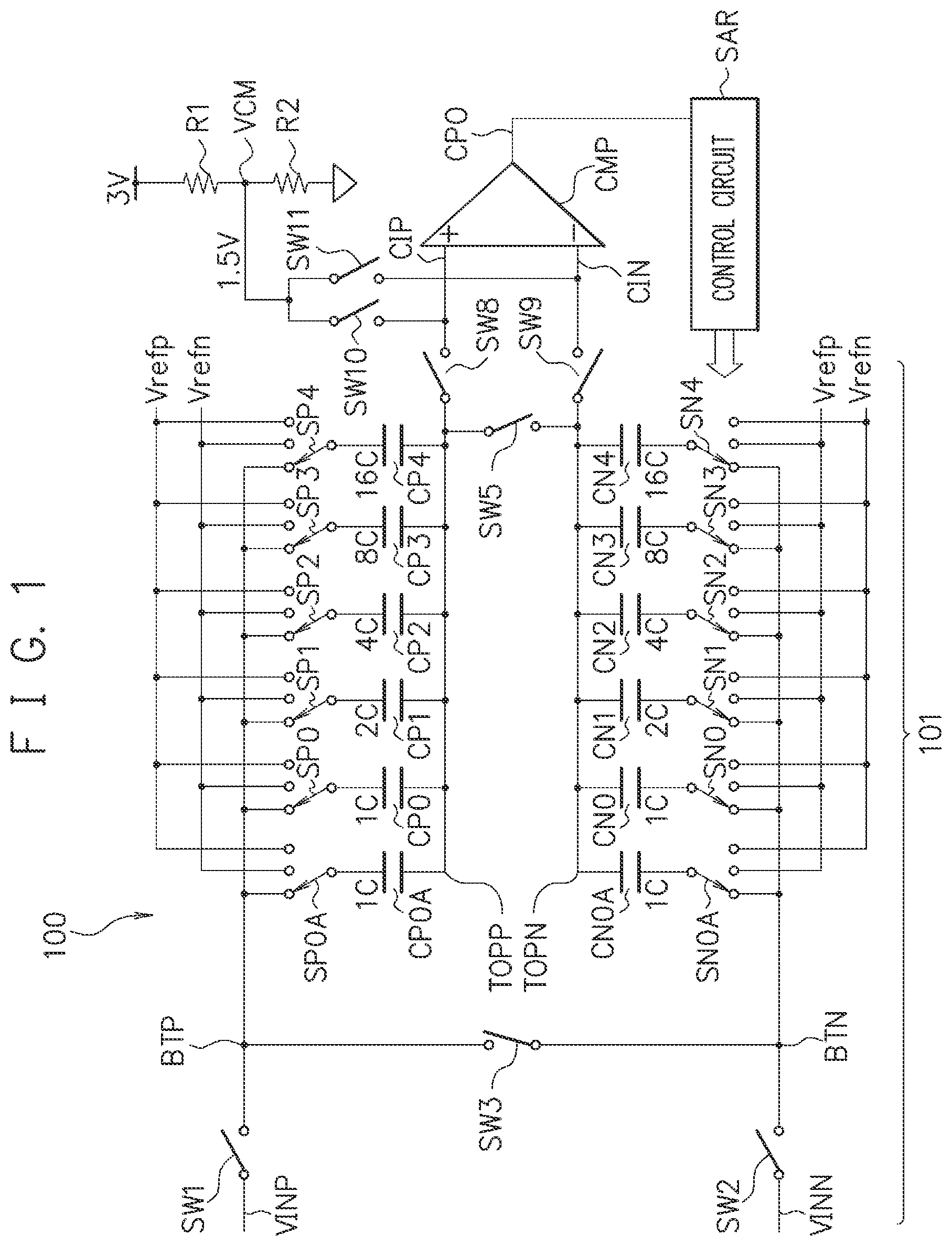
is a diagram illustrating a configuration example of an analog-to-digital converter circuit 100 according to a first embodiment. The analog-to-digital converter circuit 100 is a 4-bit analog-to-digital converter circuit that includes a sampling circuit 101 , switch circuits SW 8 to SW 11 , resistors R 1 , R 2 , a comparator CMP, and a control circuit SAR and converts an analog input voltage into a 4-bit digital code.
The sampling circuit 101 includes the switch circuits SW 1 to SW 3 and SW 5 , switch circuits SP 0 A and SP 0 to SP 4 , capacitors CP 0 A and CP 0 to CP 4 , switch circuits SN 0 A and SN 0 to SN 4 , and capacitors CN 0 A and CN 0 to CN 4 .
A relative capacitance value of the capacitors CP 0 A, CP 0 , CN 0 A, and CN 0 is 1 C. A relative capacitance value of the capacitors CP 1 and CN 1 is 2 C. A relative capacitance value of the capacitors CP 2 and CN 2 is 4 C. A relative capacitance value of the capacitors CP 3 and CN 3 is 8 C. A relative capacitance value of the capacitors CP 4 and CN 4 is 16 C.
The switch circuits SP 0 A and SP 0 to SP 4 and the capacitors CP 0 A and CP 0 to CP 4 form a 4-bit digital-to-analog converter circuit. The switch circuits SN 0 A and SN 0 to SN 4 and the capacitors CN 0 A and CN 0 to CN 4 also form a 4-bit digital-to-analog converter circuit.
Each of a plurality of the capacitors CP 0 A and CP 0 to CP 4 has a first terminal and a second terminal. Each of a plurality of the capacitors CN 0 A and CN 0 to CN 4 has a third terminal and a fourth terminal.
A top node TOPP is connected to the second terminals of a plurality of the capacitors CP 0 A and CP 0 to CP 4 . A top node TOPN is connected to the fourth terminals of a plurality of the capacitors CN 0 A and CN 0 to CN 4 .
A first input voltage, which is one of a differential input voltage, is input to an input node VINP. A second input voltage, which is the other of the differential input voltage, is input to an input node VINN. The analog-to-digital converter circuit 100 converts the analog differential input voltage into a digital code.
The switch circuit SW 1 is provided between the input node VINP and a bottom node BTP. The switch circuit SW 2 is provided between the input node VINN and a bottom node BTN. The switch circuit SW 3 is provided between the bottom node BTP and the bottom node BTN. The switch circuit SW 5 is provided between the top node TOPP and the top node TOPN.
A plurality of the switch circuits SP 0 A and SP 0 to SP 4 connect the first terminals of a plurality of the capacitors CP 0 A and CP 0 to CP 4 to the bottom node BTP, a reference voltage node Vrefp, or a reference voltage node Vrefn, respectively. The reference voltage node Vrefp is, for example, 3 V. The reference voltage node Vrefn is, for example, 0 V.
A plurality of the switch circuits SN 0 A and SN 0 to SN 4 connect the third terminals of a plurality of the capacitors CN 0 A and CN 0 to CN 4 to the bottom node BTN, the reference voltage node Vrefp, or the reference voltage node Vrefn, respectively.
The comparator CMP is a differential comparator and includes a pair of input terminals. The switch circuit SW 8 is provided between the top node TOPP and a comparison input node CIP connected to one input terminal of the comparator CMP. The switch circuit SW 9 is provided between the top node TOPN and a comparison input node CIN connected to the other input terminal of the comparator CMP. In a successive approximation operation, the comparator CMP receives the voltage of the top node TOPP via the switch circuit SW 8 and the comparison input node CIP, and receives the voltage of the top node TOPN via the switch circuit SW 9 and the comparison input node CIN. The comparator CMP compares the voltage of the top node TOPP and the voltage of the top node TOPN in the successive approximation operation.
The resistor R 1 is connected between a 3-V node and a bias voltage node VCM. The resistor R 2 is connected between the bias voltage node VCM and a 0-V node. The bias voltage node VCM is 1.5 V.
The switch circuit SW 10 is provided between the bias voltage node VCM and the comparison input node CIP. The switch circuit SW 11 is provided between the bias voltage node VCM and the comparison input node CIN.
The control circuit SAR controls a plurality of the switch circuits SP 0 A and SP 0 to SP 4 and a plurality of the switch circuits SN 0 A and SN 0 to SN 4 based on an output signal CP 0 of the comparator CMP in the successive approximation operation.
is a flowchart illustrating a processing method of the analog-to-digital converter circuit 100 in . The analog-to-digital converter circuit 100 repeatedly performs a series of operations including a reset operation at Step S 201 , a sampling operation at Step S 202 , and a successive approximation operation at Step S 203 .
At Step S 201 , the analog-to-digital converter circuit 100 performs the reset operation. The switch circuits SW 1 and SW 2 are turned off. The switch circuits SW 3 and SW 5 are turned on.
The switch circuits SP 0 A and SP 0 to SP 4 connect the first terminals of the capacitors CP 0 A and CP 0 to CP 4 to the bottom node BTP, respectively. The switch circuits SN 0 A and SN 0 to SN 4 connect the third terminals of the capacitors CN 0 A and CN 0 to CN 4 to the bottom node BTN, respectively.
The switch circuits SW 8 and SW 9 are turned off. The switch circuits SW 10 and SW 11 are turned on.
Initial charges remain in the capacitors CP 0 A and CP 0 to CP 4 and the capacitors CN 0 A and CN 0 to CN 4 . The initial charge is the charge sampled in the previous sampling operation at Step S 202 .
This reset operation does not reset the initial charges in the capacitors CP 0 A and CP 0 to CP 4 and the capacitors CN 0 A and CN 0 to CN 4 to 0 (zero), and the initial charges are redistributed. Since the switch circuits SW 3 and SW 5 are turned on, the charge amount of the capacitors CP 0 A and CP 0 to CP 4 and the charge amount of the capacitors CN 0 A and CN 0 to CN 4 are equal.
Then, at Step S 202 , the analog-to-digital converter circuit 100 performs the sampling operation of the differential input voltage. The switch circuit SW 3 is turned off. The switch circuit SW 5 remains on. The switch circuits SW 1 and SW 2 are turned on.
The switch circuits SP 0 A and SP 0 to SP 4 connect the first terminals of the capacitors CP 0 A and CP 0 to CP 4 to the bottom node BTP, respectively. The switch circuits SN 0 A and SN 0 to SN 4 connect the third terminals of the capacitors CN 0 A and CN 0 to CN 4 to the bottom node BTN, respectively.
The switch circuits SW 8 and SW 9 are turned off. The switch circuits SW 10 and SW 11 are turned on.
The input voltage of the input node VINP is applied to the first terminals of the capacitors CP 0 A and CP 0 to CP 4 . The input voltage of the input node VINN is applied to the third terminals of the capacitors CN 0 A and CN 0 to CN 4 . Since the switch circuit SW 5 is on, the top nodes TOPP and TOPN become a common potential to the input voltage of the input node VINP and the input voltage of the input node VINN.
Here, there is explained in this embodiment the case where it is known in advance that the input voltage of the input node VINP is equal to or more than the input voltage of the input node VINN.
In the capacitors CP 0 A and CP 0 to CP 4 , a charge based on the input voltage of the input node VINP is accumulated. In the capacitors CN 0 A and CN 0 to CN 4 , a charge based on the input voltage of the input node VINN is accumulated. Since the switch circuit SW 5 is on, the top nodes TOPP and TOPN become a common potential to the input voltages of the input nodes VINP and VINN.
is a diagram illustrating an equivalent circuit of the analog-to-digital converter circuit 100 in in the reset operation at Step S 201 in . A capacitor CP in corresponds to the capacitors CP 0 A and CP 0 to CP 4 in . A capacitor CN in corresponds to the capacitors CN 0 A and CN 0 to CN 4 in .
The capacitor CP is connected between the top node TOPP and the bottom node BTP. The capacitor CN is connected between the top node TOPN and the bottom node BTN.
The switch circuit SW 1 disconnects the connection between the input node VINP and the bottom node BTP. The switch circuit SW 2 disconnects the connection between the input node VINN and the bottom node BTN. The switch circuit SW 3 connects the bottom nodes BTP and BTN. The switch circuit SW 5 connects the top nodes TOPP and TOPN.
Before the reset operation at Step S 201 , initial charges remain in the capacitors CP and CN. The initial charge is the charge accumulated in the previous sampling operation at Step S 202 .
In the reset operation at Step S 201 , the switch circuits SW 1 and SW 2 are turned off, and the switch circuits SW 3 and SW 5 are turned on. Since the capacitor CP and the capacitor CN have the same capacitance value, the initial charges in the capacitors CP and CN are evenly distributed to the capacitors CP and CN.
In the sampling operation at Step S 202 , the switch circuit SW 3 is turned off and the switch circuits SW 1 and SW 2 are turned on. Then, the bottom node BTP is connected to the input node VINP. The bottom node BTN is connected to the input node VINN. The top nodes TOPP and TOPN become the common potential (VINP+VINN)/2 of the input voltages of the input nodes VINP and VINN.
is an equivalent circuit diagram including an equivalent input resistance RIN, a signal source voltage Vs, and a signal source resistance Rs of the analog-to-digital converter circuit 100 in . An input node VIN in corresponds to the input nodes VINP and VINN in . The equivalent input resistance RIN is connected between the input node VIN and the reference potential node. The signal source voltage Vs is the voltage of a signal source of the input voltage of the input node VIN. The signal source resistance Rs is the resistance of the signal source of the input voltage of the input node VIN. The equivalent input resistance RIN is connected in series with the signal source resistance Rs.
The voltage of the input node VIN is a voltage obtained by dividing the signal source voltage Vs by the signal source resistance Rs and the equivalent input resistance RIN. Therefore, if the equivalent input resistance RIN is sufficiently high, the voltage of the input node VIN becomes substantially the same as the signal source voltage Vs, and the conversion result of the analog-to-digital converter circuit 100 becomes an appropriate value.
However, when the equivalent input resistance RIN is low, the voltage of the input node VIN becomes lower than the signal source voltage Vs, and the conversion result of the analog-to-digital converter circuit 110 becomes small. Therefore, it is desirable that the equivalent input resistance RIN is sufficiently high.
In the sampling operation at Step S 202 , the charge amount that the capacitors CP and CN charge from the input nodes VINP and VINN is the difference between the charge amount in the capacitors CP and CN based on the input voltages of the input nodes VINP and VINN in the previous sampling operation and the charge amount in the capacitors CP and CN based on the input voltages of the input nodes VINP and VINN in this sampling operation. Therefore, the charge amount that the capacitors CP and CN charge from the input nodes VINP and VINN only needs to be small, so that the equivalent input resistance RIN of the analog-to-digital converter circuit 100 can be made sufficiently high to reduce the sampling operation time.
In contrast to this, there is explained the case where the charge amounts in the capacitors CP and CN are reset to 0 (zero) at Step S 201 tentatively. In this case, at Step S 202 , the capacitors CP and CN start charging from a state where the charge amount is 0 (zero). Therefore, the charge amount that the capacitors CP and CN charge from the input nodes VINP and VINN increases, resulting in a lower equivalent input resistance RIN of the analog-to-digital converter circuit 100 and a longer sampling operation time.
The sampling operation at Step S 202 is explained. The total capacitance value of the capacitors CP 0 A and CP 0 to CP 4 is 1 C+1 C+2 C+4 C+8 C+16 C=32 C. The total capacitance value of the capacitors CN 0 A and CN 0 to CN 4 is also 32 C, which is the same as the total capacitance value of the capacitors CP 0 A and CP 0 to CP 4 .
Since the switch circuit SW 5 is on, the potentials of the top nodes TOPP and TOPN become the input common potential ((VINP+VINN)/2). Here, VINP and VINN represent the potential of the input node VINP and the potential of the input node VINN, respectively.
A charge amount QSAMPP accumulated in the top node TOPP of the capacitors CP 0 A and CP 0 to CP 4 is expressed by Equation (1).
QSAMPP = - 3 2 C ( VINP - ( VINP + VINN ) / 2 ) = - 32 C ( VINP - VINN ) / 2 ( 1 )
A charge amount QSAMPN accumulated in the top node TOPN of the capacitors CN 0 A and CN 0 to CN 4 is expressed by Equation (2). QSAMPN=− 32 C (− VINP+VINN )/2 (2)
That is, by setting the potentials of the top nodes TOPP and TOPN to the input common potential (VINP+VINN)/2, the charge amounts QSAMPP and QSAMPN are equal in absolute value and opposite in positive/negative sign.
Then, at Step S 203 in , the analog-to-digital converter circuit 100 performs the successive approximation operation. The switch circuit SW 5 is turned off. Thereafter, the switch circuits SW 1 and SW 2 are also turned off. When the switch circuit SW 5 is first turned off, the top nodes TOPP and TOPN are brought into a floating state, so that the charges of the top node TOPP of the capacitors CP 0 A and CP 0 to CP 4 and the top node TOPN of the capacitors CN 0 A and CN 0 to CN 4 are preserved.
Then, the switch circuits SP 0 A and SP 0 to SP 4 are brought into a floating state. The switch circuits SN 0 A and SN 0 to SN 4 are also brought into a floating state. The switch circuit SW 3 is turned on. The switch circuits SW 10 and SW 11 are turned off. The switch circuits SW 8 and SW 9 are turned on. This completes the preparation for successive approximation by the comparator CMP.
The switch circuits SW 10 and SW 11 apply the 1.5-V bias voltage of the bias voltage node VCM to the comparison input nodes CIP and CIN of the comparator CMP during the sampling operation.
Since VINP−VINN>=0 is established, the switch circuit SP 4 connects the first terminal of the capacitor CP 4 to the reference voltage node Vrefp. The switch circuit SN 4 connects the third terminal of the capacitor CN 4 to the reference voltage node Vrefn.
The switch circuits SP 0 to SP 3 are connected to the reference voltage node Vrefp when the bit of the corresponding digital code is 1, and are connected to the reference voltage node Vrefn when the bit of the corresponding digital code is 0 (zero). To generate two's complement, the switch circuit SP 0 A, which generates a 1-bit addition value, is connected to the reference voltage node Vrefn (corresponding to the bit value “0” of the digital code). This is because there is no need to generate two's complement data.
The switch circuits SN 0 to SN 3 are connected to the reference voltage node Vrefn when the bit of the corresponding digital code is 1, and are connected to the reference voltage node Vrefp when the bit of the corresponding digital code is 0 (zero). Since VINP−VINN>=0 is established, the switch circuit SN0A is connected to the reference voltage node Vrefp (corresponding to the bit value “0” of the digital code). This is to always generate two's complement data.
Since VINP>VINN is established, the potential of the top node TOPP is always a positive number. Therefore, the switch circuit SP 0 A is connected to the reference voltage node Vrefn. Similarly, since the top node TOPN is always a negative number, the switch circuit SN 0 A is connected to the reference voltage node Vrefp.
Since VINP>VINN is assumed, as for the comparison in the comparator CMP, the comparator CMP starts comparison, for example, with VINP>VINN and the reference voltage/2, and if (VINP−VINN) is greater than the reference voltage/2, the comparator CMP compares the reference voltage×¾ and (VINP−VINN). If (VINP−VINN) is smaller than the reference voltage/2, the comparator CMP compares the reference voltage×¼ and (VINP−VINN). If (VINP−VINN) is greater than the reference voltage×¼ tentatively, the comparator CMP compares the reference voltage×⅜ and (VINP−VINN). Alternatively, if (VINP−VINN) is smaller than the reference voltage×¼, the comparator CMP compares the reference voltage×⅛ and (VINP−VINN). That is, the magnitude relation between the potential difference of (VINP−VINN) and the potential obtained by dividing the reference voltage (Vrefp−Vrefn) is determined, the range of the value of the sampled potential difference of (VINP−VINN) is sequentially narrowed, and then the final digital code is determined.
Next, there is explained a method of determining the MSB (Most Significant Bit) of the digital code. The switch circuit SP 4 is connected to the reference voltage node Vrefp. The switch circuits SP 0 to SP 2 and SP 0 A are connected to the reference voltage node Vrefn. The switch circuit SP 3 is connected to the reference voltage node Vrefp. The first terminals of the capacitors CP 0 A and CP 0 to CP 2 with the total capacitance value of 8 C are connected to the reference voltage node Vrefn. The first terminals of the capacitors CP 3 and CP 4 with the total capacitance value of 24 C are connected to the reference voltage node Vrefp. Since the charge amount QSAMPP in Equation (1) is preserved, a potential Vtp of the top node TOPP at this time is given by Equation (3). Here, Vrefp and Vrefn represent the potentials of the reference voltage nodes Vrefp and Vrefn, respectively. −24 C ( Vrefp−Vtp )+8 C ( Vtp−Vrefn )=−32 C ( VINP−VINN )/2 Vtp=− ( VINP−VINN )/2+( Vrefp+Vrefn )/2+( Vrefp−Vrefn )/(2×2) (3)
The switch circuit SN 4 is connected to the reference voltage node Vrefn. The switch circuits SN 0 to SN 2 and SN 0 A are connected to the reference voltage node Vrefp. The switch circuit SN 3 is connected to the reference voltage node VrefN. The third terminals of the capacitors CN 0 A and CN 0 to CN 2 with the total capacitance value of 8 C are connected to the reference voltage node Vrefp. The third terminals of the capacitors CN 3 and CN 4 with the total capacitance value of 24 C are connected to the reference voltage node Vrefn. Since the charge amount QSAMPN in Equation (2) is preserved, a potential Vtn of the top node TOPN at this time is given by Equation (4). −8 C ( Vrefp−Vtp )+24 C ( Vtp−Vrefn )=−32 C ( VINP−VINN )/2 Vtn =( VINP−VINN )/2+( Vrefp+Vrefn )/2−( Vrefp−Vrefn )/(2×2) (4)
The potential of the comparison input node CIP becomes the potential Vtp. The potential of the comparison input node CIN becomes the potential Vtn. The comparator CMP outputs a difference potential Vtp−Vtn between the potential Vtp and the potential Vtn as the output signal CP 0 , as illustrated in Equation (5). Vtp−Vtn=− ( VINP−VINN )+( Vrefp−Vrefn )/2 (5)
That is, the comparator CMP outputs the magnitude relation between (VINP−VINN) and (Vrefp−Vrefn)/2 as the output signal CP 0 . Based on the output signal CP 0 , the control circuit SAR determines the most significant bit of the digital code to be “1” if (VINP−VINN) is equal to or more than (Vrefp−Vrefn)/2. Further, based on the output signal CP 0 , the control circuit SAR determines the most significant bit of the digital code to be “0” if (VINP−VINN) is smaller than (Vrefp−Vrefn)/2. The most significant bit of the digital code corresponds to the switch circuits SP 3 and SN 3 .
Next, there is explained a method of determining bits after the most significant bit. There is explained a method of determining the bit (second most significant bit) corresponding to the switch circuits SP 2 and SN 2 .
It is supposed that the most significant bit of the digital code corresponding to the switch circuits SP 3 and SN 3 is determined to be 1 and (VINP−VINN) is equal to or more than (Vrefp−Vrefn)/2. In this case, the comparator CMP compares (VINP−VINN) and (Vrefp−Vrefn)×¾ and examines the magnitude relation therebetween to narrow the range of the value of (VINP−VINN).
Specifically, the switch circuit SP 4 is connected to the reference voltage node Vrefp. The switch circuits SP 0 A, SP 0 , and SP 1 are connected to the reference voltage node Vrefn. The switch circuits SP 2 and SP 3 are connected to the reference voltage node Vrefp. The first terminals of the capacitors CP 0 A, CP 0 , and CP 1 with the total capacitance value of 4 C are connected to the reference voltage node Vrefn. The first terminals of the capacitors CP 2 to CP 4 with the total capacitance value of 28 C are connected to the reference voltage node Vrefp. The potential Vtp of the top node TOPP at this time is given by Equation (6). −28 C ( Vrefp−Vtp )+4 C ( Vtp−Vrefn )=−32 C ( VINP−VINN )/2 Vtp=− ( VINP−VINN )/2+( Vrefp+Vrefn )/2+3×( Vrefp−Vrefn )/(2×4) (6)
The switch circuit SN 4 is connected to the reference voltage node Vrefn. The switch circuits SN 0 A, SN 0 , and SN 1 are connected to the reference voltage node Vrefp. The switch circuits SN 2 and SN 3 are connected to the reference voltage node Vrefn. The third terminals of the capacitors CN 0 A, CN 0 , and CN 1 with the total capacitance value of 4 C are connected to the reference voltage node Vrefp. The third terminals of the capacitors CN 2 to CN 4 with the total capacitance value of 28 C are connected to the reference voltage node Vrefn. The potential Vtn of the top node TOPN at this time is given by Equation (7). −4 C ( Vrefp−Vtp )+28 C ( Vtp−Vrefn )=32 C ( VINP−VINN )/2 Vtn =( VINP−VINN )/2+( Vrefp+Vrefn )/2−3×( Vrefp−Vrefn )/(2×4) (7)
The potential of the comparison input node CIP becomes the potential Vtp. The potential of the comparison input node CIN becomes the potential Vtn. The comparator CMP outputs a difference potential Vtp−Vtn between the potential Vtp and the potential Vtn as the output signal CP 0 , as illustrated in Equation (8). Vtp−Vtn=− ( VINP−VINN )+3×( Vrefp−Vrefn )/4 (8)
That is, the comparator CMP outputs the magnitude relation between (VINP−VINN) and (Vrefp−Vrefn)×¾ as the output signal CP 0 . Based on the output signal CP 0 , the control circuit SAR determines the second most significant bit of the digital code to be “1” if (VINP−VINN) is equal to or more than (Vrefp−Vrefn)×¾. Further, based on the output signal CP 0 , the control circuit SAR determines the second most significant bit of the digital code to be “0” if (VINP−VINN) is smaller than (Vrefp−Vrefn)×¾. The second most significant bit of the digital code corresponds to the switch circuits SP 2 and SN 2 .
In the same manner blow, the control circuit SAR can control the switch circuits SP 0 A and SP 0 to SP 4 and the switch circuits SN 0 A and SN 0 to SN 4 to determine the magnitude relation between (VINP−VINN) and the potential obtained by dividing (Vrefp−Vrefn). Thereby, the control circuit SAR can sequentially narrow the range of (VINP−VINN) to determine the final digital code.
As above, in the comparison in the comparator CMP, if (VINP−VINN) is greater than the reference voltage/2, the comparator CMP compares the reference voltage×¾ and (VINP−VINN). If (VINP−VINN) is smaller than the reference voltage/2, the comparator CMP compares the reference voltage×¼ and (VINP−VINN). Furthermore, if (VINP−VINN) is greater than the reference voltage×¼ tentatively, the comparator CMP compares the reference voltage×⅜ and (VINP−VINN). Alternatively, if (VINP−VINN) is smaller than the reference voltage×¼, the comparator CMP compares the reference voltage×⅛ and (VINP−VINN). That is, the magnitude relation between the potential difference of (VINP−VINN) and the potential obtained by dividing the reference voltage (Vrefp−Vrefn) is determined, the range of the value of the sampled potential difference of (VINP−VINN) is sequentially narrowed, and then the final digital code is determined.
After Step S 203 in , the analog-to-digital converter circuit 100 returns to Step S 201 and performs Steps S 201 to S 203 repeatedly.
As above, according to this embodiment, in the reset operation at Step S 201 , the capacitors CP and CN do not reset the charge amount to 0 (zero), but distribute the initial charge.
In the sampling operation at Step S 202 , the charge amount that the capacitors CP and CN charge from the input nodes VINP and VINN is the difference between the charge amount in the capacitors CP and CN based on the input voltages of the input nodes VINP and VINN in the previous sampling operation and the charge amount in the capacitors CP and CN based on the input voltages of the input nodes VINP and VINN in this sampling operation. Therefore, the charge amount that the capacitors CP and CN charge from the input nodes VINP and VINN only needs to be small, so that the equivalent input resistance RIN of the analog-to-digital converter circuit 100 can be made sufficiently high to reduce the sampling operation time. This makes it possible to inhibit the deterioration in accuracy of the conversion result of the analog-to-digital converter circuit 100 .
Second Embodiment
is a diagram illustrating a configuration example of an analog-to-digital converter circuit 100 according to a second embodiment. The analog-to-digital converter circuit 100 in is that resistive sub digital-to-analog converter circuits SUBDACP and SUBDACN, resistive correction digital-to-analog converter circuits CALDACP and CALDACN, capacitors CPA to CPD and CNA to CND, a switch circuit SW 4 , and a register file (memory) RF are added to the analog-to-digital converter circuit 100 in .
Further, a switch circuit SP 0 ′ and a capacitor CP 0 ′ in are provided instead of the switch circuit SP 0 A and the capacitor CP 0 A in . The relative capacitance value of the capacitor CP 0 ′ is 1 C. The switch circuit SP 0 ′ connects the first terminal of the capacitor CP 0 ′ to the resistive sub digital-to-analog converter circuit SUBDACP, the bottom node BTP, the reference voltage node Vrefp, or the reference voltage node Vrefn.
A switch circuit SN 0 ′ and a capacitor CN 0 ′ in are provided instead of the switch circuit SN 0 A and the capacitor CN 0 A in . The relative capacitance value of the capacitor CN 0 ′ is 1 C. The switch circuit SN 0 ′ connects the third terminal of the capacitor CN 0 ′ to the resistive sub digital-to-analog converter circuit SUBDACN, the bottom node BTN, the reference voltage node Vrefp, or the reference voltage node Vrefn.
Switch circuits SP 0 to SP 7 and capacitors CP 0 to CP 7 in are provided instead of the switch circuits SP 0 to SP 4 and the capacitors CP 0 to CP 4 in . Switch circuits SN 0 to SN 7 and capacitors CN 0 to CN 7 in are provided instead of the switch circuits SN 0 to SN 4 and the capacitors CN 0 to CN 4 in . These are a 7-bit capacitive main digital-to-analog converter circuit MAINDAC with positive/negative signs, which is the same as that in the first embodiment.
The analog-to-digital converter circuit 100 is a 14-bit analog-to-digital converter circuit that converts an analog input voltage into a 14-bit digital code. The 14-bit analog-to-digital converter circuit 100 includes the 7-bit capacitive main digital-to-analog converter circuit MAINDAC and the 7-bit resistive sub digital-to-analog converter circuits SUBDACP and SUBDACN. The 7-bit capacitive main digital-to-analog converter circuit MAINDAC converts a digital code of the upper 7 bits out of the 14 bits into an analog voltage. The 7-bit resistive sub digital-to-analog converter circuits SUBDACP and SUBDACN convert a digital code of the lower 7 bits out of the 14 bits into an analog voltage. This makes it possible to reduce the circuit scale of the analog-to-digital converter circuit 100 with high resolution.
The analog-to-digital converter circuit 100 further includes the resistive correction digital-to-analog converter circuits CALDACP and CALDACN. In the 14-bit or more analog-to-digital converter circuit 100 , the resistive correction digital-to-analog converter circuits CALDACP and CALDACN correct the manufacturing error of the capacitive main digital-to-analog converter circuit MAINDAC. This allows the analog-to-digital converter circuit 100 to perform a high-resolution analog-to-digital conversion.
The resistive sub digital-to-analog converter circuit SUBDACP outputs a first analog voltage to the comparison input node CIP via the capacitors CPD and CP 0 ′ based on the low-order 7-bit digital code of the 14-bit digital code.
The resistive sub digital-to-analog converter circuit SUBDACN outputs a second analog voltage to the comparison input node CIN via the capacitors CND and CN 0 ′ based on the low-order 7-bit digital code of the 14-bit digital code.
The resistive correction digital-to-analog converter circuit CALDACP is connected to the comparison input node CIP via the capacitors CPA to CPC, and corrects the voltages of the capacitors CP 0 ′ and CP 0 to CP 7 .
The resistive correction digital-to-analog converter circuit CALDACN is connected to the comparison input node CIN via the capacitors CNA to CNC, and corrects the voltages of the capacitors CN 0 ′ and CN 0 to CN 7 .
In the analog-to-digital converter circuit 100 , of 14 bits of conversion resolution and positive/negative sign bits, the high-order 7 bits and the positive/negative sign bits are determined by the capacitive main digital-to-analog converter circuit MAINDAC, and the low-order 7 bits are determined by the resistive sub digital-to-analog converter circuits SUBDACP and SUBDACN. Incidentally, the resistive sub digital-to-analog converter circuits SUBDACP and SUBDACN have two voltage outputs divided into a high-order-bit part and a low-order-bit part by resistance division in order to reduce the time constant of the output node and speed up the operation.
The high-order-bit voltage output of the resistive sub digital-to-analog converter circuit SUBDACP is connected to the top node TOPP via the capacitor CP 0 ′, and the low-order-bit voltage output of the resistive sub digital-to-analog converter circuit SUBDACP is connected to the comparison input node CIP via the capacitor CPD.
Similarly, the high-order-bit voltage output of the resistive sub digital-to-analog converter circuit SUBDACN is connected to the top node TOPN via the capacitor CN 0 ′. Further, the low-order-bit voltage output of the resistive sub digital-to-analog converter circuit SUBDACN is connected to the comparison input node CIN via the capacitor CND.
Incidentally, in the analog-to-digital converter circuit 100 , in addition to the capacitive main digital-to-analog converter circuit MAINDAC and the resistive sub digital-to-analog converter circuits SUBDACP and SUBDACN intended for performing the 14-bit conversion, the 9-bit resistive correction digital-to-analog converter circuits CALDACP and CALDACN intended for canceling capacitor mismatch are provided. These resistive correction digital-to-analog converter circuits CALDACP and CALDACN are used to implement the self-calibration function.
The resistive correction digital-to-analog converter circuit CALDACP is divided into three output voltages, which are connected to the comparison input node CIP via the capacitors CPA to CPC respectively. Further, the resistive correction digital-to-analog converter circuit CALDACN is divided into three output voltages, which are connected to the comparison input node CIN via the capacitors CNA to CNC respectively.
Here, since the resolution of the resistive correction digital-to-analog converter circuits CALDACP and CALDACN is higher than that of the resistive sub digital-to-analog converter circuits SUBDACP and SUBDACN by two bits, for example, the resistive correction digital-to-analog converter circuits CALDACP and CALDACN can make a correction for one LSB (least significant bit) of the 14 bits of the analog-to-digital conversion with a resolution four times finer than that of the resistive sub digital-to-analog converter circuits SUBDACP and SUBDACN.
In the successive approximation operation at Step S 203 in , bits are determined starting from the most significant bit of the capacitive main digital-to-analog converter circuit MAINDAC, as in the first embodiment. After the high-order 7 bits of the capacitive main digital-to-analog converter circuit MAINDAC are determined, the low-order 7 bits are determined using the resistive sub digital-to-analog converter circuits SUBDACP and SUBDACN.
During the successive approximation at Step S 203 , the resistive correction digital-to-analog converter circuits CALDACP and CALDACN operate to correct the capacitive main digital-to-analog converter circuit MAINDAC.
The capacitor mismatch of the capacitive main digital-to-analog converter circuit MAINDAC is measured when power is applied to the analog-to-digital converter circuit 100 . Data for correcting the measured capacitor mismatch are written in the register file RF.
The resistive sub digital-to-analog converter circuits SUBDACP and SUBDACN each have a voltage output for 4 bits responsible for high-order bits and a voltage output for 3 bits responsible for low-order bits.
The resistive correction digital-to-analog converter circuits CALDACP and CALDACN each have a voltage output for 3 bits responsible for high-order bits, a voltage output for 3 bits responsible for middle-order bits, and a voltage output for 3 bits responsible for low-order bits.
The outputs of the resistive sub digital-to-analog converter circuits SUBDACP and SUBDACN and the resistive correction digital-to-analog converter circuits CALDACP and CALDACN are divided to be capacitively added. Thereby, the time constants of the resistive sub digital-to-analog converter circuits SUBDACP and SUBDACN and the resistive correction digital-to-analog converter circuits CALDACP and CALDACN decrease to obtain the speeding-up effect.
The error of the capacitive main digital-to-analog converter circuit MAINDAC measured by measuring the capacitor mismatch can be converted into a correction amount (correction data) of the capacitor that is responsible for each bit. The correction data are stored in the register file RF.
At the stage of the successive approximation operation at Step S 203 , as described above, first, the trial and determination of the most significant bit are performed, and then the trial and determination of the second most significant bit are performed, and then the trial and determination of the third most significant bit are further performed. Thereafter, trials and determinations are performed for each of the bits, down to the least significant bit.
The resistive correction digital-to-analog converter circuits CALDACP and CALDACN calculate a correction amount according to the digital code input to the capacitive main digital-to-analog converter circuit MAINDAC at each stage of the successive approximation operation, and perform correction.
Next, there is explained an error correction control operation. When a trial is made on the most significant bit after the sampling operation, a correction value corresponding to the capacitor responsible for the most significant bit is output from the register file RF. The resistive correction digital-to-analog converter circuits CALDACP and CALDACN output voltages based on the value from the register file RF. At the end of the most significant bit comparison period, the comparator CMP finishes the determination and outputs “1” or “0.”
At the same time as the period for determining the following second significant bit starts, when the most significant bit is determined to be “1,” in a register, the correction value of the most significant bit from the register file RF is stored, and when it is “0,” the value of “0” is stored.
Thereafter, in the trial and determination period of the second bit, the register file RF outputs a correction value of the capacitor responsible for the second significant bit. The resistive correction digital-to-analog converter circuits CALDACP and CALDACN output voltages based on the sum of the output value of the register file RF and the value of the register.
In the same manner thereafter, the correction amount according to the digital code of the capacitive main digital-to-analog converter circuit MAINDAC is input to the resistive correction digital-to-analog converter circuits CALDACP and CALDACN. After the high-order bits are determined by the capacitive main digital-to-analog converter circuit MAINDAC, low-order bits are searched by the resistive sub digital-to-analog converter circuits SUBDACP and SUBDACN. The resistive sub digital-to-analog converter circuits SUBDACP and SUBDACN do not need to perform correction because they have a small weight with respect to the dynamic range of the analog-to-digital conversion.
According to this embodiment, the 14-bit analog-to-digital converter circuit 100 includes the 7-bit capacitive main digital-to-analog converter circuit MAINDAC, the 7-bit resistive sub digital-to-analog converter circuits SUBDACP and SUBDACN, and the 9-bit resistive correction digital-to-analog converter circuits CALDACP and CALDACN, which can convert an input analog voltage into a 14-bit digital code.
Third Embodiment
is a diagram illustrating a configuration example of a semiconductor integrated circuit 600 according to a third embodiment. The semiconductor integrated circuit 600 includes an internal circuit 610 and an analog-to-digital converter circuit 100 . The analog-to-digital converter circuit 100 is the analog-to-digital converter circuit 100 in the first or second embodiment.
The internal circuit 610 includes a p-channel field-effect transistor 601 , an n-channel field-effect transistor 602 , a resistor 603 , and a capacitor 604 . The p-channel field-effect transistor 601 and the re-channel field-effect transistor 602 form an inverter. The resistor 603 and the capacitor 604 form a first-order RC filter.
The internal circuit 610 is, for example, a duty ratio measuring circuit for a clock signal CLK. When the semiconductor integrated circuit 600 is a radio communication circuit, a phase locked loop circuit (PLL circuit) generates the clock signal CLK and supplies the clock signal CLK to a mixer circuit. The frequency of the clock signal CLK is high, which is 12 GHz or the like, for example.
The clock signal CLK is transmitted from the PLL circuit to a destination circuit while being relayed by, for example, a CMOS inverter or buffer. When the frequency of the clock signal CLK is high, the duty ratio deteriorates as the clock signal CLK passes through the relay. The duty ratio is the ratio of one-cycle period to a high-level period of the clock signal. Typically, the duty ratio of the clock signal CLK is desirably 50%.
For example, in a radio communication circuit that needs high-speed transmission of the clock signal CLK, the deterioration in the duty ratio of the clock signal CLK needs to be adjusted after the radio communication circuit is manufactured. In such a case, it is necessary to accurately measure the current duty ratio of the clock signal CLK for adjustment.
The p-channel field-effect transistor 601 and the n-channel field-effect transistor 602 are the inverter and shape the waveform of the clock signal CLK. The resistor 603 and the capacitor 604 are the first-order RC filter, and smooth the output signal of the inverter and output an analog direct-current voltage V 1 . When the duty ratio of the clock signal CLK is 50%, the direct-current voltage V 1 becomes the average value of the high level of the clock signal CLK and the low level of the clock signal CLK. The duty ratio of the clock signal CLK can be derived based on the direct-current voltage V 1 .
The internal circuit 610 outputs an analog differential input voltage based on the direct-current voltage V 1 to the analog-to-digital converter circuit 100 . The analog-to-digital converter circuit 100 converts the differential input voltage based on the input voltage V 1 into a digital code D 1 , as in the first or second embodiment.
The resistor 603 is, for example, 20 kΩ, the capacitor 604 is, for example, 20 pF, and the signal source resistance Rs in is high, which is, for example, 100 kΩ. Therefore, if the equivalent input resistance RIN in is low, the direct-current voltage V 1 decreases, failing to measure the duty ratio accurately.
Having a sufficiently high equivalent input resistance RIN, the analog-to-digital converter circuit 100 in this embodiment can inhibit the decrease in the direct-current voltage V 1 and accurately measure the duty ratio.
Note that the above embodiments merely illustrate concrete examples of implementing the present invention, and the technical scope of the present invention is not to be construed in a restrictive manner by these embodiments. That is, the present invention may be implemented in various forms without departing from the technical spirit or main features thereof.
It is possible to provide a sampling circuit and an analog-to-digital converter circuit capable of sufficiently increasing the equivalent input resistance.
All examples and conditional language provided herein are intended for the pedagogical purposes of aiding the reader in understanding the invention and the concepts contributed by the inventor to further the art, and are not to be construed as limitations to such specifically recited examples and conditions, nor does the organization of such examples in the specification relate to a showing of the superiority and inferiority of the invention. Although one or more embodiments of the present invention have been described in detail, it should be understood that the various changes, substitutions, and alterations could be made hereto without departing from the spirit and scope of the invention.
Figures (4)
Citations
This patent cites (20)
- US4803462
- US4989002
- US9432044
- US2007/0115159
- US2009/0179699
- US2010/0265113
- US2011/0234433
- US2012/0280841
- US2018/0205388
- USS64-068022
- US2001-267925
- US2007-142863
- US2010-252247
- US2011-035944
- US2011-205230
- US2012-054855
- US2014-042358
- US2014-513496
- US2017-079451
- US2007/058011