Bidirectional Direct Current Converter and Control Method Thereof
Abstract
A bidirectional direct current converter includes a controller that controls a switching transistor in the bidirectional direct current converter to reduce an inductance of an inductor, thereby reducing a size and costs of the inductor, and further reducing a size and costs of the entire bidirectional direct current converter. The bidirectional direct current converter further includes a first switching transistor, a second switching transistor, a third switching transistor, a fourth switching transistor, and a capacitor. The controller is coupled to the first switching transistor, the second switching transistor, the third switching transistor, and the fourth switching transistor. The controller performs complementary control on the first switching transistor and the third switching transistor, and performs complementary control on the second switching transistor and the fourth switching transistor.
Claims (20)
1. A bidirectional direct current converter comprising: a first direct current terminal; a second direct current terminal; a third direct current terminal; a fourth direct current terminal; a first node; a second node; a third node; an inductor comprising: a first terminal coupled to the first direct current terminal; and a second terminal coupled to the first node; a first switching transistor comprising: a first electrode coupled to the first node; and a second electrode coupled to the second node; a second switching transistor comprising: a third electrode coupled to the second node; and a fourth electrode coupled to the second direct current terminal and the fourth direct current terminal; a third switching transistor comprising: a fifth electrode coupled to the first node; and a sixth electrode coupled to the third node; a fourth switching transistor comprising: a seventh electrode coupled to the third node; and an eighth electrode coupled to the third direct current terminal; a capacitor comprising: a third terminal coupled to the third node; and a fourth terminal coupled to the second node; and a controller coupled to the first switching transistor, the second switching transistor, the third switching transistor, and the fourth switching transistor, wherein the controller is configured to: perform first complementary control on the first switching transistor and the third switching transistor so that the first switching transistor and the third switching transistor cannot be simultaneously turned on or off; perform second complementary control on the second switching transistor and the fourth switching transistor so that the second switching transistor and the fourth switching transistor cannot be simultaneously turned on or off; control a first quantity of on times of the second switching transistor to be greater than a second quantity of on times of the first switching transistor in a same cycle to reduce losses of the first switching transistor and the second switching transistor; and control a third quantity of on times of the fourth switching transistor to be greater than a fourth quantity of on times of the third switching transistor in a same cycle to reduce losses of the third switching transistor and the fourth switching transistor.
19. A control method of a bidirectional direct current converter comprising: performing, by a controller of the bidirectional direct current converter, complementary control on a first switching transistor of the bidirectional direct current converter and a third switching transistor of the bidirectional direct current converter so that the first switching transistor and the third switching transistor cannot be simultaneously turned on or off, wherein the bidirectional direct current converter further comprises a second switching transistor, a fourth switching transistor, a capacitor, and an inductor, wherein a first terminal of the inductor is coupled to a first direct current terminal of the bidirectional direct current converter, wherein a second terminal of the inductor is coupled to a first node of the bidirectional direct current converter, wherein a first electrode of the first switching transistor is coupled to the first node, wherein a second electrode of the first switching transistor is coupled to a second node of the bidirectional direct current converter, wherein a first electrode of the second switching transistor is coupled to the second node, wherein a second electrode of the second switching transistor is coupled to a second direct current terminal of the bidirectional direct current converter and a fourth direct current terminal of the bidirectional direct current converter, wherein a first electrode of the third switching transistor is coupled to the first node, wherein a second electrode of the third switching transistor is coupled to a third node, wherein a first electrode of the fourth switching transistor is coupled to the third node, wherein a second electrode of the fourth switching transistor is coupled to a third direct current terminal of the bidirectional direct current converter, wherein a first terminal of the capacitor is coupled to the third node, wherein a second terminal of the capacitor is coupled to the second node, and wherein the controller is coupled to the first switching transistor, the second switching transistor, the third switching transistor, and the fourth switching transistor; performing, by the controller, the complementary control on the second switching transistor and the fourth switching transistor so that the second switching transistor and the fourth switching transistor cannot be simultaneously turned on or off; controlling a first quantity of on times of the second switching transistor to be greater than a second quantity of on times of the first switching transistor in a same cycle to reduce losses of the first switching transistor and the second switching transistor; and controlling a third quantity of on times of the fourth switching transistor to be greater than a fourth quantity of on times of the third switching transistor in a same cycle to reduce losses of the third switching transistor and the fourth switching transistor.
20. A bidirectional direct current converter comprising: a first direct current terminal; a second direct current terminal; a third direct current terminal; a fourth direct current terminal; a first node; a second node; a third node; an inductor comprising: a first terminal coupled to the first direct current terminal; and a second terminal coupled to the first node; a first switching transistor comprising: a first electrode coupled to the first node; and a second electrode coupled to the second node; a second switching transistor comprising: a third electrode coupled to the second node; and a fourth electrode coupled to the second direct current terminal and the fourth direct current terminal; a third switching transistor comprising: a fifth electrode coupled to the first node; and a sixth electrode coupled to the third node; a fourth switching transistor comprising: a seventh electrode coupled to the third node; and an eighth electrode coupled to the third direct current terminal; a capacitor comprising: a third terminal coupled to the third node; and a fourth terminal coupled to the second node; and a controller coupled to the first switching transistor, the second switching transistor, the third switching transistor, and the fourth switching transistor, wherein the controller is configured to: perform first complementary control on the first switching transistor and the third switching transistor so that the first switching transistor and the third switching transistor cannot be simultaneously turned on or off; perform second complementary control on the second switching transistor and the fourth switching transistor so that the second switching transistor and the fourth switching transistor cannot be simultaneously turned on or off; control a first quantity of on times of the second switching transistor to be greater than a second quantity of on times of the first switching transistor in a same cycle to reduce losses of the first switching transistor and the second switching transistor; and send a first drive signal to the first switching transistor, a second drive signal to the second switching transistor, a third drive signal to the third switching transistor, and a fourth drive signal to the fourth switching transistor to implement the first complementary control on the first switching transistor and the third switching transistor and the second complementary control on the second switching transistor and the fourth switching transistor, wherein the second drive signal has first N drive pulses in each cycle of the first drive signal, wherein the fourth drive signal has second N drive pulses in each cycle of the third drive signal, wherein the inductor has N+1 charging and discharging cycles in each cycle of the first drive signal or the third drive signal, and wherein N is an integer greater than or equal to 2.
Show 17 dependent claims
2. The bidirectional direct current converter of claim 1 , further comprising, in any cycle of the first switching transistor, a delay between an on moment of the first switching transistor and an on moment of the second switching transistor.
3. The bidirectional direct current converter of claim 2 , wherein a cycle of the first switching transistor is the same as a cycle of the third switching transistor.
4. The bidirectional direct current converter of claim 1 , wherein the controller is further configured to send a first drive signal to the first switching transistor, a second drive signal to the second switching transistor, a third drive signal to the third switching transistor, and a fourth drive signal to the fourth switching transistor to implement the first complementary control on the first switching transistor and the third switching transistor and the second complementary control on the second switching transistor and the fourth switching transistor, wherein the second drive signal has first N drive pulses in each cycle of the first drive signal, wherein the fourth drive signal has second N drive pulses in each cycle of the third drive signal, wherein the inductor has N+1 charging and discharging cycles in each cycle of the first drive signal or the third drive signal, and wherein N is an integer greater than or equal to 2.
5. The bidirectional direct current converter of claim 4 , wherein the first N drive pulses are in low level time periods of each cycle of the first drive signal.
6. The bidirectional direct current converter of claim 4 , wherein a first part of pulses of the second N drive pulses are in low level time periods of each cycle of the third drive signal, and wherein a second part of pulses of the second N drive pulses are in high level time periods of each cycle of the third drive signal.
7. The bidirectional direct current converter of claim 4 , wherein frequencies corresponding to at least two of the first N drive pulses or the second N drive pulses are different.
8. The bidirectional direct current converter of claim 7 , wherein a frequency corresponding to each of the first N drive pulses or the second N drive pulses is different.
9. The bidirectional direct current converter of claim 7 , wherein a pulse width of each of the first N drive pulses or the second N drive pulses is the same.
10. The bidirectional direct current converter of claim 4 , wherein N≥3.
11. The bidirectional direct current converter of claim 10 , wherein frequencies of first N−1 drive pulses of the first N drive pulses or the second N drive pulses are the same, and wherein a frequency of a last drive pulse of the first N drive pulses or the second N drive pulses is less than the frequencies.
12. The bidirectional direct current converter of claim 4 , wherein, in each cycle of the first drive signal, a rising edge of a first drive pulse of the first N drive pulses is behind a falling edge of the first drive signal.
13. The bidirectional direct current converter of claim 12 , wherein, in each cycle of the third drive signal, a rising edge of a first drive pulse of the second N drive pulses is in front of a falling edge of the third drive signal.
14. The bidirectional direct current converter of claim 13 , wherein, in each cycle of the first drive signal, a time between a rising edge of the first drive signal and the rising edge of the first drive pulse of the first N drive pulses is a first lag time, or wherein, in each cycle of the third drive signal, a time between a rising edge of the third drive signal and the rising edge of the first drive pulse of the second N drive pulses is a second lag time.
15. The bidirectional direct current converter of claim 14 , wherein the controller is further configured to control, in each charging cycle of the inductor and discharging cycle of the inductor, a charging current of the inductor to be equal to a discharging current of the inductor to obtain the first lag time or the second lag time.
16. The bidirectional direct current converter of claim 15 , wherein the controller is further configured to: obtain the first lag time or the second lag time based on a first voltage of the bidirectional direct current converter, a second voltage of the bidirectional direct current converter, a third voltage of the capacitor, and a cycle of the first drive signal or a cycle of the third drive signal, wherein: the first voltage indicates a first input voltage of the bidirectional direct current converter and the second voltage indicates a first output voltage of the bidirectional direct current converter; or the first voltage indicates a second output voltage of the bidirectional direct current converter and the second voltage indicates a second input voltage of the bidirectional direct current converter.
17. The bidirectional direct current converter of claim 16 , wherein the controller is further configured to obtain the first lag time or the second lag time according to a formula, wherein the formula comprises: ( V 1 +V c −V 2 ) D 1 T sw =( V 2 −V 1 ) D 2 T sw , wherein the first lag time or the second lag time is (D 1 +D 2 )T sw , wherein V 1 represents the first voltage, wherein V 2 represents the second voltage, wherein V c represents the third voltage, wherein T sw represents the cycle of the first drive signal or the cycle of the third drive signal, wherein D 1 represents a duty cycle of the first drive signal, and wherein D 2 T sw represents a delay time between the rising edge of the first drive pulse of the first N drive pulses and the falling edge of the first drive signal.
18. The bidirectional direct current converter of claim 14 , wherein the controller is further configured to: obtain the first lag time or the second lag time based on a loss of the first switching transistor or a loss of the second switching transistor; obtain the first lag time or the second lag time based on a loss of the third switching transistor or a loss of the fourth switching transistor; obtain the first lag time or the second lag time based on a ripple current of the inductor and the loss of at least one of the first switching transistor or the second switching transistor; or obtain the first lag time or the second lag time based on the ripple current and the loss of at least one of the third switching transistor or the fourth switching transistor, wherein each cycle of the first drive signal is the same as each cycle of the third drive signal, and wherein the bidirectional direct current converter further comprises a fifth switching transistor comprising: a fifth terminal coupled to the fourth terminal; and a sixth terminal coupled to the second node.
Full Description
Show full text →
CROSS-REFERENCE TO RELATED APPLICATION
This claims priority to Chinese Patent Application No. 202111489706.5 filed on Dec. 8, 2021, which is hereby incorporated by reference in its entirety.
TECHNICAL FIELD
This disclosure relates to the field of energy technologies, and in particular, to a bidirectional direct current converter and a control method thereof in the field of energy technologies.
BACKGROUND
A direct current converter is a power electronic apparatus that can convert a direct current of one voltage class into a direct current of another voltage class. Direct current converters are usually classified into unidirectional direct current converters and bidirectional direct current converters. A unidirectional direct current converter is a direct current converter that can perform only unidirectional power transmission, and a bidirectional direct current converter is a direct current converter that can perform bidirectional power transmission.
For the bidirectional direct current converter, how to reduce an inductance of an inductor in the bidirectional direct current converter by controlling a switching transistor in the bidirectional direct current converter, to reduce a size and costs of the inductor becomes a technical problem that needs to be resolved urgently.
SUMMARY
This disclosure provides a bidirectional direct current converter and a control method thereof. A controller performs complementary control on a first switching transistor and a third switching transistor, and performs complementary control on a second switching transistor and a fourth switching transistor, to reduce an inductance of an inductor, thereby reducing a size and costs of the inductor, and further reducing a size and costs of the entire bidirectional direct current converter.
According to a first aspect, this disclosure provides a bidirectional direct current converter. The bidirectional direct current converter may include a first switching transistor, a second switching transistor, a third switching transistor, a fourth switching transistor, a capacitor, an inductor, and a controller.
Optionally, the bidirectional direct current converter may include a first direct current terminal, a second direct current terminal, a third direct current terminal, and a fourth direct current terminal.
In an example, the first direct current terminal and the second direct current terminal may constitute an input terminal of the bidirectional direct current converter, and the third direct current terminal and the fourth direct current terminal may constitute an output terminal of the bidirectional direct current converter. Therefore, the bidirectional direct current converter may implement forward power transmission by using the four direct current terminals.
In another example, the third direct current terminal and the fourth direct current terminal may constitute an input terminal of the bidirectional direct current converter, and the first direct current terminal and the second direct current terminal may constitute an output terminal of the bidirectional direct current converter. Therefore, the bidirectional direct current converter may implement reverse power transmission by using the four direct current terminals.
Further, a first terminal of the inductor may be configured to connect to the first direct current terminal, and a second terminal of the inductor may be configured to connect to a first node. A first electrode of the first switching transistor may be configured to connect to the first node, and a second electrode of the first switching transistor may be configured to connect to a second node. A first electrode of the second switching transistor may be configured to connect to the second node, and a second electrode of the second switching transistor may be configured to connect to the second direct current terminal and the fourth direct current terminal. A first electrode of the third switching transistor may be configured to connect to the first node, and a second electrode of the third switching transistor may be configured to connect to a third node. A first electrode of the fourth switching transistor may be configured to connect to the third node, and a second electrode of the fourth switching transistor may be configured to connect to the third direct current terminal. A first terminal of the capacitor may be configured to connect to the third node, and a second terminal of the capacitor may be configured to connect to the second node. The controller may be configured to connect to the first switching transistor, the second switching transistor, the third switching transistor, and the fourth switching transistor.
Based on the foregoing connection relationship, the controller may be configured to perform complementary control on the first switching transistor and the third switching transistor, and perform complementary control on the second switching transistor and the fourth switching transistor.
The complementary control may be used to indicate that two switching transistors in complementary control cannot be simultaneously turned on or off. For example, the first switching transistor and the third switching transistor cannot be simultaneously turned on or off, and the second switching transistor and the fourth switching transistor cannot be simultaneously turned on or off.
That is, the controller may control the first switching transistor and the third switching transistor not to be simultaneously turned on or off, and the controller may further control the second switching transistor and the fourth switching transistor not to be simultaneously turned on or off.
The controller may be further configured to control a quantity of on times of the second switching transistor to be greater than a quantity of on times of the first switching transistor in a same cycle. It may also be understood as that, in one cycle, the controller may control a switching frequency of the second switching transistor to be greater than a switching frequency of the first switching transistor, thereby reducing losses of the first switching transistor and the second switching transistor.
In this disclosure, the controller may control the quantity of on times of the second switching transistor to be different from the quantity of on times of the first switching transistor in a same cycle. This can increase a quantity of charging and discharging times of the inductor in one cycle, that is, increase a charging and discharging frequency of the inductor. Therefore, the inductor with a small inductance may be used while a same ripple current percentage of the inductor is ensured. In addition, the inductor with a small inductance has a small size and low costs. This can reduce a size and costs of the bidirectional direct current converter. When the size of the bidirectional direct current converter is reduced, power density of the bidirectional direct current converter can be increased.
In a possible implementation, in any cycle of the first switching transistor, there may be a delay between an on moment of the first switching transistor and an on moment of the second switching transistor. That is, the first switching transistor and the second switching transistor are not simultaneously turned on in any cycle.
Further, a cycle of the first switching transistor may be the same as a cycle of the third switching transistor.
In a possible implementation, the controller is further configured to control a quantity of on times of the fourth switching transistor to be greater than a quantity of on times of the third switching transistor in a same cycle. It may also be understood as that, in one cycle, the controller may control a switching frequency of the fourth switching transistor to be greater than a switching frequency of the third switching transistor, thereby reducing losses of the third switching transistor and the fourth switching transistor.
It may be understood that the controller controls the quantity of on times of the fourth switching transistor to be different from the quantity of on times of the third switching transistor in a same cycle. Similarly, this can increase a quantity of charging and discharging times of the inductor in one cycle, that is, increase a charging and discharging frequency of the inductor. Therefore, the inductor with a small inductance may be used while a same ripple current percentage of the inductor is ensured. In addition, the inductor with a small inductance has a small size and low costs. This can reduce a size and costs of the bidirectional direct current converter. When the size of the bidirectional direct current converter is reduced, power density of the bidirectional direct current converter can be increased.
In a possible implementation, the controller is configured to send a first drive signal to the first switching transistor, send a second drive signal to the second switching transistor, send a third drive signal to the third switching transistor, and send a fourth drive signal to the fourth switching transistor. That is, the controller may send the drive signals to the switching transistors, to implement complementary control on the first switching transistor and the third switching transistor, and implement complementary control on the second switching transistor and the fourth switching transistor.
For example, the controller sends the first drive signal to the first switching transistor, to control on and off of the first switching transistor. It may be understood that the first drive signal may be used to indicate the first switching transistor to be turned on, or the first drive signal may be used to indicate the first switching transistor to be turned off.
Similarly, the controller sends the second drive signal to the second switching transistor, to control on and off of the second switching transistor. It may be understood that the second drive signal may be used to indicate the second switching transistor to be turned on, or the second drive signal may be used to indicate the second switching transistor to be turned off.
The controller sends the third drive signal to the third switching transistor, to control on and off of the third switching transistor. It may be understood that the third drive signal may be used to indicate the third switching transistor to be turned on, or the third drive signal may be used to indicate the third switching transistor to be turned off.
The controller sends the fourth drive signal to the fourth switching transistor, to control on and off of the fourth switching transistor. It may be understood that the fourth drive signal may be used to indicate the fourth switching transistor to be turned on, or the fourth drive signal may be used to indicate the fourth switching transistor to be turned off.
Optionally, when the first drive signal is at a high level, the first switching transistor may be turned on, and when the first drive signal is at a low level, the first switching transistor may be turned off.
Similarly, when the third drive signal is at a high level, the third switching transistor may be turned on, and when the third drive signal is at a low level, the third switching transistor may be turned off.
It may be understood that the first drive signal may be complementary to the third drive signal. That is, when the first drive signal is at a high level, the third drive signal may be at a low level. Similarly, when the first drive signal is at a low level, the third drive signal may be at a high level.
It should be noted that there is a delay interval between a falling edge of the first drive signal and a rising edge of the third drive signal. That is, in a range of the delay interval, the first switching transistor and the third switching transistor are simultaneously turned off.
Optionally, when the second drive signal is at a high level, the second switching transistor may be turned on, and when the second drive signal is at a low level, the second switching transistor may be turned off.
Similarly, when the fourth drive signal is at a high level, the fourth switching transistor may be turned on, and when the fourth drive signal is at a low level, the fourth switching transistor may be turned off.
It may be understood that the second drive signal may be complementary to the fourth drive signal. That is, when the second drive signal is at a high level, the fourth drive signal may be at a low level. Similarly, when the second drive signal is at a low level, the fourth drive signal may be at a high level.
Optionally, in any cycle of the first switching transistor, there may be a delay between the on moment of the first switching transistor and the on moment of the second switching transistor. Therefore, in each cycle of the first drive signal, a rising edge of a first drive pulse of N drive pulses in the second drive signal may be behind the falling edge of the first drive signal. That is, there is a delay time (namely, a delay) between a first drive pulse of two drive pulses in the second drive signal and the first drive signal.
Similarly, in each cycle of the third drive signal, a rising edge of a first drive pulse of N drive pulses in the fourth drive signal may be in front of a falling edge of the third drive signal. That is, there is a delay between a first drive pulse of two drive pulses in the fourth drive signal and the third drive signal.
In a possible implementation, the cycle of the first switching transistor may be the same as the cycle of the third switching transistor. Therefore, a cycle of the first drive signal may be the same as a cycle of the third drive signal.
Further, the second drive signal may have N drive pulses in each cycle of the first drive signal, that is, the second drive signal and the first drive signal may be two asymmetric drive signals.
Similarly, the fourth drive signal may have N drive pulses in each cycle of the third drive signal, that is, the fourth drive signal pulse-width modulation (PWM) and the third drive signal PWM are two asymmetric drive signals.
Further, the inductor may have N+1 charging and discharging cycles in each cycle of the first drive signal or the third drive signal, where N is an integer greater than or equal to 2 (for example, N is greater than 3).
Therefore, the inductor has at least three charging and discharging cycles in each cycle. The controller increases a charging and discharging frequency of the inductor in each cycle (namely, frequency increase), thereby reducing the inductance of the inductor, and reducing the size and the costs of the inductor.
It should be noted that there is also a delay interval between a falling edge of the first drive pulse of the N drive pulses in the fourth drive signal and the rising edge of the first drive pulse of the N drive pulses in the second drive signal. In a range of the delay interval, the second switching transistor and the fourth switching transistor are simultaneously turned off.
Because the second drive signal may have N drive pulses in each cycle of the first drive signal, a cycle of the second drive signal is different from the cycle of the first drive signal. Similarly, because the fourth drive signal may also have N drive pulses in each cycle of the third drive signal, a cycle of the fourth drive signal is different from the cycle of the third drive signal.
In the bidirectional direct current converter provided in this disclosure, the controller may send the first drive signal and the second drive signal that are asymmetric to the first switching transistor and the second switching transistor, and send the third drive signal and the fourth drive signal that are asymmetric to the third switching transistor and the fourth switching transistor, so that a quantity of charging and discharging times of the inductor in each cycle of the first drive signal or the third drive signal is increased, that is, the charging and discharging frequency of the inductor is increased. Therefore, the inductor with a small inductance may be used while a same ripple current percentage of the inductor is ensured. In addition, the inductor with a small inductance has a small size and low costs. This can reduce a size and costs of the bidirectional direct current converter. When the size of the bidirectional direct current converter is reduced, power density of the bidirectional direct current converter can be increased.
In addition, in this disclosure, the asymmetric drive signals are sent to the first switching transistor and the second switching transistor, and the asymmetric drive signals are sent to the third switching transistor and the fourth switching transistor, so that a state of the first switching transistor is opposite to a state of the third switching transistor (that is, the first switching transistor is complementary to the third switching transistor), and a state of the second switching transistor is opposite to a state of the fourth switching transistor (that is, the second switching transistor is complementary to the fourth switching transistor). Further, current sharing or complement is implemented between a branch in which the first switching transistor and the second switching transistor are located and a branch in which the third switching transistor and the fourth switching transistor are located (that is, between two branches), so that a voltage of the capacitor remains stable.
In a possible implementation, the N drive pulses in the second drive signal may be in low level time periods of each cycle of the first drive signal.
Certainly, the N drive pulses in the second drive signal may alternatively be in high level time periods of each cycle of the first drive signal. Alternatively, the N drive pulses in the second drive signal may be divided into a first part of drive pulses and a second part of drive pulses. The first part of drive pulses may be in low level time periods of each cycle of the first drive signal, and the second part of drive pulses may be in high level time periods of each cycle of the first drive signal. This is not limited in this disclosure.
In another possible implementation, the N drive pulses in the fourth drive signal may be divided into a first part of drive pulses and a second part of drive pulses. The first part of drive pulses may be in low level time periods of each cycle of the third drive signal, and the second part of drive pulses may be in high level time periods of each cycle of the third drive signal.
Certainly, the N drive pulses in the fourth drive signal may be all in low level time periods of each cycle of the third drive signal, or may be all in high level time periods of each cycle of the third drive signal. This is not limited in this disclosure.
Optionally, frequencies corresponding to at least two of the N drive pulses in the second drive signal or the fourth drive signal may be different.
It should be noted that a frequency of a drive pulse is inversely proportional to a cycle of the drive pulse. Therefore, cycles corresponding to the at least two of the N drive pulses in the second drive signal or the fourth drive signal are different, so that the frequencies corresponding to the at least two of the N drive pulses in the second drive signal or the fourth drive signal are different.
Further, a frequency corresponding to each of the N drive pulses in the second drive signal or the fourth drive signal may be different.
Optionally, a pulse width of each of the N drive pulses in the second drive signal or the fourth drive signal may be the same.
It should be noted that there is no correspondence between pulse widths and frequencies that are of different drive pulses of the N drive pulses in the second drive signal or the fourth drive signal. That is, when pulse widths of different drive pulses are the same, frequencies of the different drive pulses may be the same or different. Similarly, when frequencies of different drive pulses are the same, pulse widths of the different drive pulses may be the same or different.
In a possible implementation, when N≥3, frequencies of first N−1 drive pulses of the N drive pulses in the second drive signal or the fourth drive signal may be the same, and a frequency of a last drive pulse of the N drive pulses in the second drive signal may be less than the frequencies of the first N−1 drive pulses.
In a possible implementation, a lag time in this disclosure may be defined in the following two manners:
Manner 1: In each cycle of the first drive signal, a time between a rising edge of the first drive signal and the rising edge of the first drive pulse of the N drive pulses in the second drive signal may be a lag time.
Manner 2: In each cycle of the third drive signal, a time between the rising edge of the third drive signal and the rising edge of the first drive pulse of the N drive pulses in the fourth drive signal may be a lag time.
Certainly, the lag time may alternatively be defined in another manner. This is not limited in this disclosure.
The following describes in detail an obtaining process of the lag time.
In an example, because a ripple current of the inductor is affected by the lag time, the controller may obtain the lag time based on the ripple current of the inductor. To reduce the ripple current of the inductor, in each charging and discharging cycle of the inductor, the controller may control a charging current of the inductor to be equal to a discharging current of the inductor to obtain the lag time.
Further, in each charging and discharging cycle of the inductor, the controller may control the charging current of the inductor to be equal to the discharging current of the inductor to obtain the lag time.
Further, the controller may obtain the lag time based on a first voltage of the bidirectional direct current converter, a second voltage of the bidirectional direct current converter, the voltage of the capacitor, and the cycle of the first drive signal/the third drive signal.
Optionally, the first voltage may be used to indicate an input voltage of the bidirectional direct current converter, and the second voltage may be used to indicate an output voltage of the bidirectional direct current converter. Alternatively, the first voltage may be used to indicate an output voltage of the bidirectional direct current converter, and the second voltage may be used to indicate an input voltage of the bidirectional direct current converter.
Further, the controller may obtain the lag time (D 1 +D 2 )T sw according to the following formula: ( V 1 +V c −V 2 ) D 1 T sw =( V 2 −V 1 ) D 2 T sw
In the formula, V 1 may represent the first voltage of the bidirectional direct current converter, V 2 may represent the second voltage of the bidirectional direct current converter, V c may represent the voltage of the capacitor, T sw may represent the cycle of the first drive signal or the third drive signal, D 1 may represent a duty cycle of the first drive signal, and D 2 T sw may represent the delay time between the rising edge of the first drive pulse of the N drive pulses in the second drive signal and the falling edge of the first drive signal.
In another example, the controller may obtain the lag time based on the loss of the first switching transistor and/or the loss of the second switching transistor, or may obtain the lag time based on the loss of the third switching transistor and/or the loss of the fourth switching transistor.
That is, the controller may obtain the lag time based on only the loss of the first switching transistor, based on only the loss of the second switching transistor, or based on both the loss of the first switching transistor and the loss of the second switching transistor.
Similarly, the controller may obtain the lag time based on only the loss of the third switching transistor, based on only the loss of the fourth switching transistor, or based on both the loss of the third switching transistor and the loss of the fourth switching transistor.
In another example, the controller may obtain the lag time based on the ripple current of the inductor and the loss of at least one of the first switching transistor and the second switching transistor (namely, the loss of the first switching transistor and/or the loss of the second switching transistor), or may obtain the lag time based on the ripple current of the inductor and the loss of at least one of the third switching transistor and the fourth switching transistor (namely, the loss of the third switching transistor and/or the loss of the fourth switching transistor).
It should be noted that the lag time may alternatively be obtained by using another process in this disclosure. This is not limited in this disclosure.
In this disclosure, a loss generated by the bidirectional direct current converter may be reduced based on losses of different switching transistors, thereby improving conversion efficiency of the bidirectional direct current converter.
In a possible implementation, the bidirectional direct current converter provided in this disclosure may further include a fifth switching transistor. A first terminal of the fifth switching transistor may be configured to connect to the second terminal of the capacitor, and a second terminal of the fifth switching transistor may be configured to connect to the second node.
Optionally, the fifth switching transistor may use an insulated gate field-effect transistor, an insulated gate bipolar transistor, a bidirectional switch, or the like. Certainly, the fifth switching transistor may alternatively use another type of controllable power device. A type of the fifth switching transistor is not limited in this disclosure.
In this disclosure, the fifth switching transistor is turned on and off, to protect the second switching transistor from being damaged due to excessively large voltage stress.
In another possible implementation, considering pre-charging of the capacitor and an abrupt change of a voltage of a bus in the bidirectional direct current converter, the bidirectional direct current converter provided in this disclosure may further include a first diode and a second diode.
Optionally, an anode of the first diode may be configured to connect to the second node, a cathode of the first diode may be configured to connect to a midpoint of the second voltage, an anode of the second diode may be configured to connect to the midpoint of the second voltage, and a cathode of the second diode may be configured to connect to the third node.
It may be understood that a function of the first diode is to clamp a voltage drop borne by the second switching transistor, to prevent the second switching transistor from bearing a voltage of an entire direct current bus when the fourth switching transistor is turned on. Similarly, a function of the second diode is to clamp a voltage drop borne by the fourth switching transistor, to prevent the fourth switching transistor from bearing a voltage of an entire direct current bus when the second switching transistor is turned on. Therefore, the first diode and the second diode may be referred to as clamping diodes.
Further, the first switching transistor, the second switching transistor, the third switching transistor, and the fourth switching transistor separately use any one of the insulated gate field-effect transistor, the insulated gate bipolar transistor, and the bidirectional switch.
Optionally, the first diode and the second diode each may alternatively be replaced with another type of power device. In this case, the controller only needs to send corresponding drive signals, so that the switching transistors implement working modes of the diodes. Details are not described in this disclosure again.
According to a second aspect, this disclosure provides an electronic device. The electronic device may include a bidirectional direct current converter. For detailed descriptions of the bidirectional direct current converter, refer to the foregoing descriptions. Details are not described in this disclosure again.
According to a third aspect, this disclosure provides a control method of a bidirectional direct current converter. The bidirectional direct current converter may include a first switching transistor, a second switching transistor, a third switching transistor, a fourth switching transistor, a capacitor, an inductor, and a controller.
Optionally, the bidirectional direct current converter may include a first direct current terminal, a second direct current terminal, a third direct current terminal, and a fourth direct current terminal.
In an example, the first direct current terminal and the second direct current terminal may constitute an input terminal of the bidirectional direct current converter, and the third direct current terminal and the fourth direct current terminal may constitute an output terminal of the bidirectional direct current converter. Therefore, the bidirectional direct current converter may implement forward power transmission by using the four direct current terminals.
In another example, the third direct current terminal and the fourth direct current terminal may constitute an input terminal of the bidirectional direct current converter, and the first direct current terminal and the second direct current terminal may constitute an output terminal of the bidirectional direct current converter. Therefore, the bidirectional direct current converter may implement reverse power transmission by using the four direct current terminals.
Further, a first terminal of the inductor may be configured to connect to the first direct current terminal, and a second terminal of the inductor may be configured to connect to a first node. A first electrode of the first switching transistor may be configured to connect to the first node, and a second electrode of the first switching transistor may be configured to connect to a second node. A first electrode of the second switching transistor may be configured to connect to the second node, and a second electrode of the second switching transistor may be configured to connect to the second direct current terminal and the fourth direct current terminal. A first electrode of the third switching transistor may be configured to connect to the first node, and a second electrode of the third switching transistor may be configured to connect to a third node. A first electrode of the fourth switching transistor may be configured to connect to the third node, and a second electrode of the fourth switching transistor may be configured to connect to the third direct current terminal. A first terminal of the capacitor may be configured to connect to the third node, and a second terminal of the capacitor may be configured to connect to the second node. The controller may be configured to connect to the first switching transistor, the second switching transistor, the third switching transistor, and the fourth switching transistor.
Therefore, the control method of the bidirectional direct current converter may include the following. The controller performs complementary control on the first switching transistor and the third switching transistor, and performs complementary control on the second switching transistor and the fourth switching transistor.
The complementary control is used to indicate that two switching transistors in complementary control cannot be simultaneously turned on or off. For example, the first switching transistor and the third switching transistor cannot be simultaneously turned on or off, and the second switching transistor and the fourth switching transistor cannot be simultaneously turned on or off.
Optionally, the controller controls a quantity of on times of the second switching transistor to be greater than a quantity of on times of the first switching transistor in a same cycle. It may also be understood as that, in one cycle, the controller may control a switching frequency of the second switching transistor to be greater than a switching frequency of the first switching transistor, thereby reducing losses of the first switching transistor and the second switching transistor.
In the control method provided in this disclosure, the controller controls the quantity of on times of the second switching transistor to be different from the quantity of on times of the first switching transistor in a same cycle. This can increase a quantity of charging and discharging times of the inductor in one cycle, that is, increase a charging and discharging frequency of the inductor. Therefore, the inductor with a small inductance may be used while a same ripple current percentage of the inductor is ensured. In addition, the inductor with a small inductance has a small size and low costs. This can reduce a size and costs of the bidirectional direct current converter. When the size of the bidirectional direct current converter is reduced, power density of the bidirectional direct current converter can be increased.
In a possible implementation, in any cycle of the first switching transistor, there may be a delay between an on moment of the first switching transistor and an on moment of the second switching transistor. That is, the first switching transistor and the second switching transistor are not simultaneously turned on in any cycle.
Further, a cycle of the first switching transistor may be the same as a cycle of the third switching transistor.
In a possible implementation, the control method may further include the following. The controller controls a quantity of on times of the fourth switching transistor to be greater than a quantity of on times of the third switching transistor in a same cycle. It may also be understood as that, in one cycle, the controller may control a switching frequency of the fourth switching transistor to be greater than a switching frequency of the third switching transistor, thereby reducing losses of the third switching transistor and the fourth switching transistor.
It may be understood that the controller controls the quantity of on times of the fourth switching transistor to be different from the quantity of on times of the third switching transistor in a same cycle. Similarly, this can increase a quantity of charging and discharging times of the inductor in one cycle, that is, increase a charging and discharging frequency of the inductor. Therefore, the inductor with a small inductance may be used while a same ripple current percentage of the inductor is ensured. In addition, the inductor with a small inductance has a small size and low costs. This can reduce a size and costs of the bidirectional direct current converter. When the size of the bidirectional direct current converter is reduced, power density of the bidirectional direct current converter can be increased.
It should be understood that technical solutions of the second aspect and the third aspect of this disclosure are consistent with the technical solution of the first aspect of this disclosure, and beneficial effects obtained by the aspects and corresponding feasible implementations are similar. Details are not described herein again.
BRIEF DESCRIPTION OF DRAWINGS
To describe some of the technical solutions in this disclosure more clearly, the following briefly describes the accompanying drawings for describing embodiments. It is clear that the accompanying drawings in the following description show some embodiments of this disclosure, and a person of ordinary skill in the art may still derive other drawings from these accompanying drawings without creative efforts.
is a schematic diagram of a structure of a bidirectional direct current converter according to an embodiment of this disclosure;
is a schematic diagram of waveforms of asymmetric drive signals according to an embodiment of this disclosure;
is a schematic diagram of waveforms of symmetric drive signals according to an embodiment of this disclosure;
is a schematic diagram of waveforms of symmetric drive signals according to an embodiment of this disclosure;
is a schematic diagram of waveforms of a first drive signal and a second drive signal according to an embodiment of this disclosure;
is a schematic diagram of waveforms of a first drive signal and a second drive signal according to an embodiment of this disclosure;
is a schematic diagram of waveforms of a first drive signal and a second drive signal according to an embodiment of this disclosure;
is a schematic diagram of waveforms of a first drive signal and a second drive signal according to an embodiment of this disclosure;
is a schematic diagram of waveforms of a first drive signal and a second drive signal according to an embodiment of this disclosure;
is a schematic diagram of waveforms of a first drive signal and a second drive signal according to an embodiment of this disclosure;
is a schematic diagram of waveforms of a first drive signal and a second drive signal according to an embodiment of this disclosure;
is a schematic diagram of waveforms of a first drive signal and a second drive signal according to an embodiment of this disclosure;
is a schematic diagram of a structure of a bidirectional direct current converter according to an embodiment of this disclosure;
is a schematic diagram of a structure of a bidirectional direct current converter according to an embodiment of this disclosure; and
is a schematic diagram of a structure of a bidirectional direct current converter according to an embodiment of this disclosure.
DESCRIPTION OF EMBODIMENTS
The following describes technical solutions of this disclosure with reference to the accompanying drawings.
To make the objectives, technical solutions, and advantages of this disclosure clearer, the following clearly describes the technical solutions in this disclosure with reference to the accompanying drawings in this disclosure. It is clear that the described embodiments are merely a part rather than all of embodiments of this disclosure. All other embodiments obtained by a person of ordinary skill in the art based on embodiments of this disclosure without creative efforts shall fall within the protection scope of this disclosure.
The terms “first”, “second”, and the like in the specification embodiments, claims, and accompanying drawings of this disclosure are merely used for distinguishing descriptions, and cannot be understood as indicating or implying relative importance, or as indicating or implying a sequence. In addition, the terms “include”, “have”, and any variation thereof are intended to cover non-exclusive inclusions, for example, a series of steps or units are included. Methods, systems, products, or devices are not limited to those clearly listed steps or units, and other steps or units that are not clearly listed or that are inherent to these processes, methods, products, or devices may be included.
It should be understood that, in this disclosure, “at least one (item)” refers to one or more, and “a plurality of” refers to two or more. The term “and/or” is used for describing an association relationship between associated objects, and represents that three relationships may exist. For example, “A and/or B” may represent the following three cases: only A exists, only B exists, and both A and B exist, where A and B may be singular or plural. The character “/” usually indicates an “or” relationship between associated objects. “At least one of the following items (pieces)” or a similar expression thereof indicates any combination of these items, including a single item (piece) or any combination of a plurality of items (pieces). For example, at least one item (piece) of a, b, or c may represent: a, b, c, “a and b”, “a and c”, “b and c”, or “a, b, and c”, where a, b, and c may be singular or plural.
An embodiment of this disclosure provides a bidirectional direct current converter, as shown in . In , the bidirectional direct current converter 1 may include a first switching transistor S 1 , a second switching transistor S 2 , a third switching transistor S 3 , a fourth switching transistor S 4 , a capacitor C (flying capacitor), an inductor L, and a controller (not shown in ).
Optionally, the bidirectional direct current converter 1 may include a first direct current terminal DC 1 , a second direct current terminal DC 2 , a third direct current terminal DC 3 , and a fourth direct current terminal DC 4 .
In an example, the first direct current terminal DC 1 and the second direct current terminal DC 2 may constitute an input terminal of the bidirectional direct current converter 1 , and the third direct current terminal DC 3 and the fourth direct current terminal DC 4 may constitute an output terminal of the bidirectional direct current converter 1 . Therefore, in , V 1 (namely, a first voltage that is a voltage between the first direct current terminal DC 1 and the second direct current terminal DC 2 ) may be used to indicate an input voltage of the bidirectional direct current converter 1 , and V 2 (namely, a second voltage that is a voltage between the third direct current terminal DC 3 and the fourth direct current terminal DC 4 ) may be used to indicate an output voltage of the bidirectional direct current converter 1 .
In another example, the third direct current terminal DC 3 and the fourth direct current terminal DC 4 may constitute an input terminal of the bidirectional direct current converter 1 , and the first direct current terminal DC 1 and the second direct current terminal DC 2 may constitute an output terminal of the bidirectional direct current converter 1 . Therefore, in , V 1 (namely, a first voltage) may be used to indicate an output voltage of the bidirectional direct current converter 1 , and V 2 (namely, a second voltage) may be used to indicate an input voltage of the bidirectional direct current converter 1 .
It can be learned that the bidirectional direct current converter provided in this embodiment of this disclosure can implement bidirectional power transmission. To be specific, a power may be transmitted from the first direct current terminal DC 1 and the second direct current terminal DC 2 that are used as the input terminal to the third direct current terminal DC 3 and the fourth direct current terminal DC 4 that are used as the output terminal, to implement forward power transmission (that is, the bidirectional direct current converter performs forward working).
Similarly, a power may alternatively be transmitted from the third direct current terminal DC 3 and the fourth direct current terminal DC 4 that are used as the input terminal to the first direct current terminal DC 1 and the second direct current terminal DC 2 that are used as the output terminal, to implement reverse power transmission (that is, the bidirectional direct current converter performs reverse working).
A first terminal of the inductor L (namely, a left terminal of the inductor L in ) may be connected to the first direct current terminal DC 1 , and a second terminal of the inductor L may be connected to a node A (namely, a first node). A first electrode of the first switching transistor S 1 (namely, an electrode that is of the first switching transistor S 1 and that is close to the node A in ) may be connected to the node A, and a second electrode of the first switching transistor S 1 (namely, an electrode that is of the first switching transistor S 1 and that is close to a node B in ) may be connected to the node B (namely, a second node). A first electrode of the second switching transistor S 2 (namely, an electrode that is of the second switching transistor S 2 and that is close to the node B in ) is connected to the node B, a second electrode of the second switching transistor S 2 (namely, an electrode that is of the second switching transistor S 2 and that is away from the node B in ) may be connected to a node E, and the node E is connected to the second direct current terminal DC 2 and the fourth direct current terminal DC 4 . A first electrode of the third switching transistor S 3 (namely, an electrode that is of the third switching transistor S 3 and that is close to the node A in ) may be connected to the node A, and a second electrode of the third switching transistor S 3 (namely, an electrode that is of the third switching transistor S 3 and that is close to a node D in ) is connected to the node D (namely, a third node). A first electrode of the fourth switching transistor S 4 (namely, an electrode that is of the fourth switching transistor S 4 and that is close to the node D in ) is connected to the node D, and a second electrode of the fourth switching transistor S 4 (namely, an electrode that is of the fourth switching transistor S 4 and that is close to the third direct current terminal DC 3 in ) may be connected to the third direct current terminal DC 3 . A first terminal of the capacitor C (which may be a positive terminal of the capacitor C) may be connected to the node D, and a second terminal of the capacitor C (which may be a negative terminal of the capacitor C) may be connected to the node B. The controller may be connected to the first switching transistor S 1 , the second switching transistor S 2 , the third switching transistor S 3 , and the fourth switching transistor S 4 .
It can be learned from the foregoing connection relationship that the bidirectional direct current converter provided in this embodiment of this disclosure is a three-level direct current converter, and three levels are implemented by using a topology of the bidirectional direct current converter. In addition, voltage stress of a power device may be reduced, so that a high-level voltage output can be implemented by using a power device with a low withstand voltage level.
Optionally, the controller may be configured to perform complementary control on the first switching transistor S 1 and the third switching transistor S 3 , and perform complementary control on the second switching transistor S 2 and the fourth switching transistor S 4 .
The complementary control is used to indicate that two switching transistors in complementary control cannot be simultaneously turned on or off. For example, the first switching transistor S 1 and the third switching transistor S 3 cannot be simultaneously turned on or off, and the second switching transistor S 2 and the fourth switching transistor S 4 cannot be simultaneously turned on or off.
That is, the controller may control the first switching transistor S 1 and the third switching transistor S 3 not to be simultaneously turned on or off, and the controller may further control the second switching transistor S 2 and the fourth switching transistor S 4 not to be simultaneously turned on or off.
Further, the controller may be further configured to control a quantity of on times of the second switching transistor S 2 to be greater than a quantity of on times of the first switching transistor S 1 in a same cycle. It may also be understood as that, in one cycle, the controller may control a switching frequency of the second switching transistor S 2 to be greater than a switching frequency of the first switching transistor S 1 , thereby reducing losses of the first switching transistor S 1 and the second switching transistor S 2 .
In this embodiment of this disclosure, the controller may control the quantity of on times of the second switching transistor to be different from the quantity of on times of the first switching transistor in a same cycle. This can increase a quantity of charging and discharging times of the inductor in one cycle, that is, increase a charging and discharging frequency of the inductor. Therefore, the inductor with a small inductance may be used while a same ripple current percentage of the inductor is ensured. In addition, the inductor with a small inductance has a small size and low costs. This can reduce a size and costs of the bidirectional direct current converter. When the size of the bidirectional direct current converter is reduced, power density of the bidirectional direct current converter can be increased.
In a possible implementation, in any cycle of the first switching transistor S 1 , there may be a delay between an on moment of the first switching transistor S 1 and an on moment of the second switching transistor S 2 . That is, the first switching transistor S 1 and the second switching transistor S 2 are not simultaneously turned on in any cycle.
Further, a cycle of the first switching transistor S 1 may be the same as a cycle of the third switching transistor S 3 .
In a possible implementation, the controller may be further configured to control a quantity of on times of the fourth switching transistor S 4 to be greater than a quantity of on times of the third switching transistor S 3 in a same cycle. It may also be understood as that, in one cycle, the controller may control a switching frequency of the fourth switching transistor S 4 to be greater than a switching frequency of the third switching transistor S 3 , thereby reducing losses of the fourth switching transistor S 4 and the third switching transistor S 3 .
It may be understood that the controller controls the quantity of on times of the fourth switching transistor to be different from the quantity of on times of the third switching transistor in a same cycle. Similarly, this can increase a quantity of charging and discharging times of the inductor in one cycle, that is, increase a charging and discharging frequency of the inductor. Therefore, the inductor with a small inductance may be used while a same ripple current percentage of the inductor is ensured. In addition, the inductor with a small inductance has a small size and low costs. This can reduce a size and costs of the bidirectional direct current converter. When the size of the bidirectional direct current converter is reduced, power density of the bidirectional direct current converter can be increased.
In a possible implementation, the controller may send a first drive signal (which may be represented by PWM 1 ) to the first switching transistor S 1 , send a second drive signal (which may be represented by PWM 2 ) to the second switching transistor S 2 , send a third drive signal (which may be represented by PWM 3 ) to the third switching transistor S 3 , and send a fourth drive signal (which may be represented by PWM 4 ) to the fourth switching transistor S 4 .
Optionally, a cycle (namely, each cycle) of the first drive signal PWM 1 and a cycle (namely, each cycle) of the third drive signal PWM 3 are the same, and may be both represented by T sw (that is, T sw represents the cycle of the first drive signal PWM 1 or the third drive signal PWM 3 ).
The second drive signal PWM 2 may have N drive pulses in each cycle of the first drive signal PWM 1 , that is, the second drive signal PWM 2 and the first drive signal PWM 1 are two asymmetric drive signals.
Similarly, the fourth drive signal PWM 4 may also have N drive pulses in each cycle of the third drive signal PWM 3 , that is, the fourth drive signal PWM 4 and the third drive signal PWM 3 are two asymmetric drive signals.
Because the second drive signal PWM 2 may have N drive pulses in each cycle of the first drive signal PWM 1 , a cycle of the second drive signal PWM 2 is different from the cycle of the first drive signal PWM 1 . Similarly, because the fourth drive signal PWM 4 may also have N drive pulses in each cycle of the third drive signal PWM 3 , a cycle of the fourth drive signal PWM 4 is also different from the cycle of the third drive signal PWM 3 .
Optionally, the controller sends the first drive signal PWM 1 to the first switching transistor S 1 , to control on and off of the first switching transistor S 1 . It may be understood that the first drive signal PWM 1 may be used to indicate the first switching transistor S 1 to be turned on, or the first drive signal PWM 1 may be used to indicate the first switching transistor S 1 to be turned off.
Similarly, the controller sends the second drive signal PWM 2 to the second switching transistor S 2 , to control on and off of the second switching transistor S 2 . It may be understood that the second drive signal PWM 2 may be used to indicate the second switching transistor S 2 to be turned on, or the second drive signal PWM 2 may be used to indicate the second switching transistor S 2 to be turned off.
The controller sends the third drive signal PWM 3 to the third switching transistor S 3 , to control on and off of the third switching transistor S 3 . It may be understood that the third drive signal PWM 3 may be used to indicate the third switching transistor S 3 to be turned on, or the third drive signal PWM 3 may be used to indicate the third switching transistor S 3 to be turned off.
The controller sends the fourth drive signal PWM 4 to the fourth switching transistor S 4 , to control on and off of the fourth switching transistor S 4 . It may be understood that the fourth drive signal PWM 4 may be used to indicate the fourth switching transistor S 4 to be turned on, or the fourth drive signal PWM 4 may be used to indicate the fourth switching transistor S 4 to be turned off.
The inductor L has N+1 charging and discharging cycles in each cycle (namely, T sw ) of the first drive signal PWM 1 or the third drive signal PWM 3 , where N may be an integer greater than or equal to 2. A value of N is not limited in this embodiment of this disclosure.
Therefore, the inductor L has at least three charging and discharging cycles in each cycle T sw . The controller increases a charging and discharging frequency of the inductor L in each cycle T sw (namely, frequency increase), thereby reducing the inductance of the inductor L, and reducing the size and the costs of the inductor L.
For example, when N is equal to 2, the inductor L may have three charging and discharging cycles in each cycle T sw , and when N is equal to 3, the inductor L may have four charging and discharging cycles in each cycle T sw .
For ease of description, the following uses N=2 as an example for detailed description.
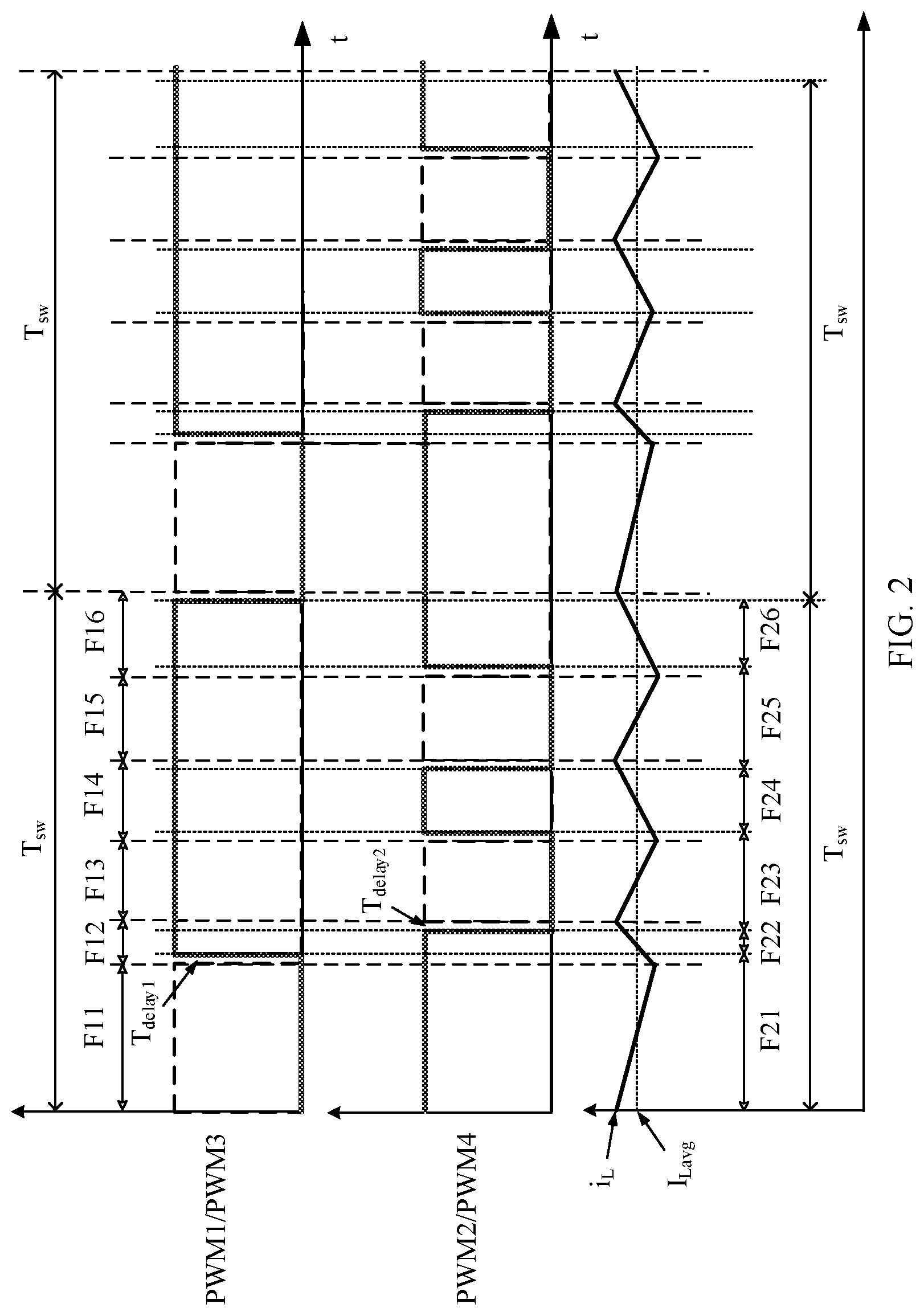
is a schematic diagram of waveforms of four drive signals (namely, the first drive signal PWM 1 (dashed line), the second drive signal PWM 2 (dashed line), the third drive signal PWM 3 (solid line), and the fourth drive signal PWM 4 (solid line)). In , i L represents an actual current (solid line) of the inductor L, and I Lavg may represent an average current (dashed line) of the inductor L.
Optionally, when the first drive signal PWM 1 is at a high level, the first switching transistor S 1 may be turned on, and when the first drive signal PWM 1 is at a low level, the first switching transistor S 1 may be turned off.
Similarly, when the third drive signal PWM 3 is at a high level, the third switching transistor S 3 may be turned on, and when the third drive signal PWM 3 is at a low level, the third switching transistor S 3 may be turned off.
It may be understood that the first drive signal PWM 1 may be complementary to the third drive signal PWM 3 . That is, when the first drive signal PWM 1 is at a high level, the third drive signal PWM 3 may be at a low level. Similarly, when the first drive signal PWM 1 is at a low level, the third drive signal PWM 3 may be at a high level.
It should be noted that there is a delay interval (namely, T delay1 in ) between a falling edge of the first drive signal PWM 1 and a rising edge of the third drive signal PWM 3 . That is, in a range of the delay interval T delay1 , the first switching transistor S 1 and the third switching transistor S 3 are simultaneously turned off.
Optionally, when the second drive signal PWM 2 is at a high level, the second switching transistor S 2 may be turned on, and when the second drive signal PWM 2 is at a low level, the second switching transistor S 2 may be turned off.
Similarly, when the fourth drive signal PWM 2 is at a high level, the fourth switching transistor S 4 may be turned on, and when the fourth drive signal PWM 4 is at a low level, the fourth switching transistor S 4 may be turned off.
It may be understood that the second drive signal PWM 2 may be complementary to the fourth drive signal PWM 4 . That is, when the second drive signal PWM 2 is at a high level, the fourth drive signal PWM 4 may be at a low level. Similarly, when the second drive signal PWM 2 is at a low level, the fourth drive signal PWM 4 may be at a high level.
It should be noted that there is also a delay interval (namely, T delay2 in ) between a falling edge of a first drive pulse of the N drive pulses in the fourth drive signal PWM 4 and a rising edge of a first drive pulse of the N drive pulses in the second drive signal PWM 2 . In a range of the delay interval T delay2 , the second switching transistor S 2 and the fourth switching transistor S 4 are simultaneously turned off.
In a possible implementation, in any cycle of the first switching transistor S 1 , there may be a delay between the on moment of the first switching transistor S 1 and the on moment of the second switching transistor S 2 . Therefore, in each cycle of the first drive signal PWM 1 , the rising edge of the first drive pulse of the N drive pulses in the second drive signal PWM 2 may be behind the falling edge of the first drive signal PWM 1 . That is, there is a delay time (namely, a delay) between a first drive pulse of two drive pulses in the second drive signal PWM 2 and the first drive signal PWM 1 .
Similarly, in each cycle of the third drive signal PWM 3 , a rising edge of the first drive pulse of the N drive pulses in the fourth drive signal PWM 4 may be in front of a falling edge of the third drive signal PWM 3 . That is, there is a delay between a first drive pulse of two drive pulses in the fourth drive signal PWM 4 and the third drive signal PWM 3 .
In the following, the third direct current terminal DC 3 and the fourth direct current terminal DC 4 in are used as the input terminal of the bidirectional direct current converter, and the first direct current terminal DC 1 and the second direct current terminal DC 2 are used as the output terminal of the bidirectional direct current converter, to describe a control process of the controller for the four switching transistors. When the bidirectional direct current converter performs reverse working, the bidirectional direct current converter is a buck converter.
In , a time period F 11 , a time period F 12 , a time period F 13 , a time period F 14 , a time period F 15 , and a time period F 16 are different time periods of one cycle T sw of the first drive signal PWM 1 . The six time periods (namely, the time period F 11 , the time period F 12 , the time period F 13 , the time period F 14 , the time period F 15 , and the time period F 16 ) constitute one cycle T sw of the first drive signal PWM 1 .
It can be seen from that, in each cycle of the first drive signal PWM 1 , a rising edge of the first drive pulse of the two drive pulses in the second drive signal PWM 2 may be behind the falling edge of the first drive signal PWM 1 . That is, there is a delay time (namely, a delay) between the first drive pulse of the two drive pulses in the second drive signal PWM 2 and the first drive signal PWM 1 .
Optionally, the second drive signal PWM 2 may have two drive pulses in each cycle T sw of the first drive signal PWM 1 , and the second drive signal PWM 2 has two drive pulses in low level time periods of each cycle T sw of the first drive signal PWM 1 . Therefore, in one cycle T sw of the first drive signal PWM 1 , the inductor L has three charging and discharging cycles in total, that is, the inductor L completes three times of charging and discharging in one cycle T sw of the first drive signal PWM 1 . This increases the charging and discharging frequency of the inductor L.
One cycle T sw of the first drive signal PWM 1 may be used as an example. The time period F 11 is a high level time period of the first drive signal PWM 1 , and the time period F 12 , the time period F 13 , the time period F 14 , the time period F 15 , and the time period F 16 each are a low level time period of the first drive signal PWM 1 .
The second drive signal PWM 2 has drive pulses in the time period F 13 and the time period F 15 , that is, the second drive signal PWM 2 is at a high level in the time period F 13 and the time period F 15 . The second drive signal PWM 2 does not have a drive pulse in the time period F 11 , the time period F 12 , the time period F 14 , and the time period F 16 , that is, the second drive signal PWM 2 is at a low level in the time period F 11 , the time period F 12 , the time period F 14 , and the time period F 16 .
That is, the second drive signal PWM 2 has two drive pulses in the low level time periods of one cycle T sw of the first drive signal PWM 1 , that is, a drive pulse corresponding to the time period F 13 and a drive pulse corresponding to the time period F 15 . Therefore, the inductor L completes charging and discharging in the time period F 11 and the time period F 12 for the first time, completes charging and discharging in the time period F 13 and the time period F 14 for the second time, and completes charging and discharging in the time period F 15 and the time period F 16 for the third time. It can be learned that the inductor L completes charging and discharging for three times in total. This increases the charging and discharging frequency of the inductor L in one cycle T sw of the first drive signal PWM 1 , and further reduces a ripple current in the inductor L.
The following describes in detail, with reference to , that the controller controls the second drive signal PWM 2 to have two drive pulses in the low level time periods of each cycle T sw of the first drive signal PWM 1 to increase the charging and discharging frequency of the inductor L.
For ease of description, the following uses one cycle T sw of the first drive signal PWM 1 as an example to describe a charging and discharging process of the inductor L.
As shown in , in the time period F 11 , the first drive signal PWM 1 is at a high level, and the second drive signal PWM 2 is at a low level. To be specific, the controller may control the first switching transistor S 1 to be turned on and control the second switching transistor S 2 to be turned off, so that the inductor L is discharged, and i L gradually decreases. In the time period F 12 , both the first drive signal PWM 1 and the second drive signal PWM 2 are at a low level. To be specific, the controller may control both the first switching transistor S 1 and the second switching transistor S 2 to be turned off, so that the inductor L is charged, and i L gradually increases. In this case, the inductor L completes charging and discharging for the first time.
In the time period F 13 , the first drive signal PWM 1 is at a low level, and the second drive signal PWM 2 is at a high level. To be specific, the controller may control the first switching transistor S 1 to be turned off and control the second switching transistor S 2 to be turned on, so that the inductor L is discharged, and i L gradually decreases. In the time period F 14 , both the first drive signal PWM 1 and the second drive signal PWM 2 are at a low level. To be specific, the controller may control both the first switching transistor S 1 and the second switching transistor S 2 to be turned off, so that the inductor L is charged, and i L gradually increases. In this case, the inductor L completes charging and discharging for the second time.
In the time period F 15 , the first drive signal PWM 1 is at a low level, and the second drive signal PWM 2 is at a high level. To be specific, the controller may control the first switching transistor S 1 to be turned off and control the second switching transistor S 2 to be turned on, so that the inductor L is discharged, and i L gradually decreases. In the time period F 16 , both the first drive signal PWM 1 and the second drive signal PWM 2 are at a low level. To be specific, the controller may control both the first switching transistor S 1 and the second switching transistor S 2 to be turned off, so that the inductor L is charged, and i L gradually increases. In this case, the inductor L completes charging and discharging for the third time.
Therefore, the inductor L completes charging and discharging for three times in total in one cycle T sw of the first drive signal PWM 1 .
The controller sends the first drive signal PWM 1 and the second drive signal PWM 2 that are asymmetric to the first switching transistor S 1 and the second switching transistor S 2 , to increase the quantity of charging and discharging times of the inductor L in each cycle of the first drive signal PWM 1 , that is, increase the charging and discharging frequency of the inductor L. Therefore, the inductor with a small inductance may be used while a same ripple current percentage of the inductor L is ensured. In addition, the inductor with a small inductance has a small size and low costs. This can reduce a size and costs of the bidirectional direct current converter.
Still refer to . A time period F 21 , a time period F 22 , a time period F 23 , a time period F 24 , a time period F 25 , and a time period F 26 are different time periods of one cycle T sw of the third drive signal PWM 3 . The six time periods (namely, the time period F 21 , the time period F 22 , the time period F 23 , the time period F 24 , the time period F 25 , and the time period F 26 ) constitute one cycle T sw of the third drive signal PWM 3 .
It can be further seen from that, in each cycle of the third drive signal PWM 3 , a rising edge of the first drive pulse of the two drive pulses in the fourth drive signal PWM 4 may be in front of the falling edge of the third drive signal PWM 3 . That is, there is also a delay between the first drive pulse of the two drive pulses in the fourth drive signal PWM 4 and the third drive signal PWM 3 .
Optionally, the fourth drive signal PWM 4 may have two drive pulses in each cycle T sw of the third drive signal PWM 3 . One of the two drive pulses in the fourth drive signal PWM 4 (namely, a first part of drive pulses in a plurality of drive pulses in the fourth drive signal PWM 4 ) is in a low level time period of each cycle T sw of the third drive signal PWM 3 , and the other of the two drive pulses in the fourth drive signal PWM 4 (namely, a second part of drive pulses in the plurality of drive pulses in the fourth drive signal PWM 4 ) is in a high level time period of each cycle T sw of the third drive signal PWM 3 . Therefore, in one cycle T sw of the third drive signal PWM 3 , the inductor L has three charging and discharging cycles in total, that is, the inductor L completes three times of charging and discharging in one cycle T sw of the third drive signal PWM 3 . Similarly, this can increase the charging and discharging frequency of the inductor L.
One cycle T sw of the third drive signal PWM 3 may be used as an example. The time period F 21 is a low level time period of the third drive signal PWM 3 , and the time period F 22 , the time period F 23 , the time period F 24 , the time period F 25 , and the time period F 26 each are a high level time period of the third drive signal PWM 3 .
The fourth drive signal PWM 4 has drive pulses in the time period F 21 , the time period F 22 , the time period F 24 , and the time period F 26 , that is, the fourth drive signal PWM 4 is at a high level in the time period F 21 , the time period F 22 , the time period F 24 , and the time period F 26 . The fourth drive signal PWM 4 does not have a drive pulse in the time period F 23 and the time period F 25 , that is, the fourth drive signal PWM 4 is at a low level in the time period F 23 and the time period F 25 .
That is, the fourth drive signal PWM 4 has one drive pulse in a low level time period of one cycle T sw of the third drive signal PWM 3 , namely, a drive pulse corresponding to the time period F 21 . In addition, the fourth drive signal PWM 4 has two drive pulses in high level time periods of one cycle T sw of the third drive signal PWM 3 , namely, a drive pulse corresponding to the time period F 24 and a drive pulse corresponding to the time period F 26 .
Therefore, the inductor L completes charging and discharging in the time period F 21 to the time period F 23 for the first time, completes charging and discharging in the time period F 24 and the time period F 26 for the second time, and completes charging and discharging in the time period F 26 for the third time. It can be learned that the inductor L completes charging and discharging for three times in total. This increases the charging and discharging frequency of the inductor L in one cycle T sw of the third drive signal PWM 3 , and further reduces a ripple current in the inductor L.
The following describes in detail, with reference to , that the controller controls the fourth drive signal PWM 4 to have one drive pulse in the low level time period and two drive pulses in the high level time periods of each cycle T sw of the third drive signal PWM 3 to increase the charging and discharging frequency of the inductor L.
For ease of description, the following uses one cycle T sw of the third drive signal PWM 3 as an example to describe a charging and discharging process of the inductor L.
As shown in , in the time period F 21 , the third drive signal PWM 3 is at a low level, and the fourth drive signal PWM 4 is at a high level. To be specific, the controller may control the third switching transistor S 3 to be turned off and control the fourth switching transistor S 4 to be turned on, so that the inductor L is discharged, and i L gradually decreases. In the time period F 22 , both the third drive signal PWM 3 and the fourth drive signal PWM 4 are at a high level. To be specific, the controller may control both the third switching transistor S 3 and the fourth switching transistor S 4 to be turned on, so that the inductor L is charged, and i L gradually increases. In this case, the inductor L completes charging and discharging for the first time.
In the time period F 23 , the third drive signal PWM 3 is at a high level, and the fourth drive signal PWM 4 is at a low level. To be specific, the controller may control the third switching transistor S 3 to be turned on and control the fourth switching transistor S 4 to be turned off, so that the inductor L is discharged, and i L gradually decreases. In the time period F 24 , both the third drive signal PWM 3 and the fourth drive signal PWM 4 are at a high level. To be specific, the controller may control both the third switching transistor S 3 and the fourth switching transistor S 4 to be turned on, so that the inductor L is charged, and i L gradually increases. In this case, the inductor L completes charging and discharging for the second time.
In the time period F 25 , the third drive signal PWM 3 is at a high level, and the fourth drive signal PWM 4 is at a low level. To be specific, the controller may control the third switching transistor S 3 to be turned on and control the fourth switching transistor S 4 to be turned off, so that the inductor L is discharged, and i L gradually decreases. In the time period F 26 , both the third drive signal PWM 3 and the fourth drive signal PWM 4 are at a high level. To be specific, the controller may control both the third switching transistor S 3 and the fourth switching transistor S 4 to be turned on, so that the inductor L is charged, and i L gradually increases. In this case, the inductor L completes charging and discharging for the third time.
Therefore, the inductor L completes charging and discharging for three times in total in one cycle T sw of the third drive signal PWM 3 .
The controller sends the third drive signal PWM 3 and the fourth drive signal PWM 4 that are asymmetric to the third switching transistor S 3 and the fourth switching transistor S 4 , to increase the quantity of charging and discharging times of the inductor L in each cycle of the third drive signal PWM 3 , that is, increase the charging and discharging frequency of the inductor L. Therefore, the inductor with a small inductance may be used while a same ripple current percentage of the inductor L is ensured. In addition, the inductor with a small inductance has a small size and low costs. This can reduce a size and costs of the bidirectional direct current converter.
In the bidirectional direct current converter provided in this embodiment of this disclosure, the controller can send the asymmetric drive signals to the first switching transistor and the second switching transistor, and send the asymmetric drive signals to the third switching transistor and the fourth switching transistor. This increases the charging and discharging frequency of the inductor, thereby reducing the costs of the inductor, and further reducing the size and the costs of the bidirectional direct current converter. When the size of the bidirectional direct current converter is reduced, power density of the bidirectional direct current converter can be increased.
In addition, in this embodiment of this disclosure, the asymmetric drive signals are sent to the first switching transistor and the second switching transistor, and the asymmetric drive signals are sent to the third switching transistor and the fourth switching transistor, so that a state of the first switching transistor is opposite to a state of the third switching transistor (that is, the first switching transistor is complementary to the third switching transistor), and a state of the second switching transistor is opposite to a state of the fourth switching transistor (that is, the second switching transistor is complementary to the fourth switching transistor). Further, current sharing or complement is implemented between a branch in which the first switching transistor and the second switching transistor are located and a branch in which the third switching transistor and the fourth switching transistor are located (that is, between two branches), so that a voltage of the capacitor remains stable.
To verify advantages of the asymmetric drive signals shown in , the following performs description with reference to diagrams of waveforms of symmetric drive signals provided in and .
When the bidirectional direct current converter shown in performs forward working (to be specific, the first direct current terminal DC 1 and the second direct current terminal DC 2 are used as the input terminal of the bidirectional direct current converter, and the third direct current terminal DC 3 and the fourth direct current terminal DC 4 are used as the output terminal of the bidirectional direct current converter), the bidirectional direct current converter is a boost converter. Therefore, the third switching transistor S 3 and the fourth switching transistor S 4 in the bidirectional direct current converter shown in may be separately equivalent to a diode. In this case, the controller may send drive signals to only the first switching transistor S 1 and the second switching transistor S 2 .
A diagram of waveforms of the first drive signal PWM 1 sent by the controller to the first switching transistor S 1 and the second drive signal PWM 2 sent by the controller to the second switching transistor S 2 is shown in . It can be seen from that the first drive signal PWM 1 and the second drive signal PWM 2 are symmetric, that is, cycles of the two drive signals are the same, and duty cycles are also the same.
It can be seen from that, in one cycle T sw of the first drive signal PWM 1 , the first drive signal PWM 1 may have one drive pulse, the second drive signal PWM 2 may also have one drive pulse, and the inductor L may perform charging and discharging for two times. i L has two cycles. To be specific, when the first drive signal PWM 1 or the second drive signal PWM 2 is at a high level, the inductor L is charged, and i L gradually increases, and when the first drive signal PWM 1 or the second drive signal PWM 2 is at a low level, the inductor L is discharged, and i L gradually decreases.
However, in , the first drive signal PWM 1 and the second drive signal PWM 2 are asymmetric drive signals. In one cycle T sw of the first drive signal PWM 1 , the first drive signal PWM 1 has one drive pulse, the second drive signal PWM 2 has at least two drive pulses, and the inductor L performs charging and discharging for at least three times.
It can be learned from comparison between and that, in this embodiment of this disclosure, the asymmetric drive signals can be used to increase a frequency of one (namely, the second drive signal) of the drive signals, thereby increasing the charging and discharging frequency of the inductor L and reducing the inductance of the inductor.
When the bidirectional direct current converter shown in performs reverse working (to be specific, the third direct current terminal DC 3 and the fourth direct current terminal DC 4 are used as the input terminal of the bidirectional direct current converter, and the first direct current terminal DC 1 and the second direct current terminal DC 2 are used as the output terminal of the bidirectional direct current converter), the bidirectional direct current converter is a buck converter. Therefore, the first switching transistor S 1 and the second switching transistor S 2 in the bidirectional direct current converter shown in may be separately equivalent to a diode. In this case, the controller may send drive signals to only the third switching transistor S 3 and the fourth switching transistor S 4 .
A diagram of waveforms of the third drive signal PWM 3 sent by the controller to the third switching transistor S 3 and the fourth drive signal PWM 4 sent by the controller to the fourth switching transistor S 4 is shown in . It can be seen from that the third drive signal PWM 3 and the fourth drive signal PWM 4 are symmetric, that is, cycles of the two drive signals are the same, and duty cycles are also the same.
It can be seen from that, in one cycle T sw of the third drive signal PWM 3 , the third drive signal PWM 3 may have one drive pulse, and the fourth drive signal PWM 4 may also have one drive pulse. i L has two cycles. To be specific, the inductor L may perform two times of charging and discharging as follows. When the third drive signal PWM 3 is at a low level and the fourth drive signal PWM 4 is at a high level, the inductor L is charged for the first time and i L gradually increases, when both the third drive signal PWM 3 and the fourth drive signal are at a high level, the inductor L is discharged for the first time and i L gradually decreases, and the inductor L completes charging and discharging for the first time, and when the third drive signal is at a high level and the fourth drive signal PWM 4 is at a low level, the inductor L is charged for the second time and i L gradually increases, when the third drive signal is at a low level and the fourth drive signal PWM 4 is at a low level, the inductor L is discharged for the second time and i L gradually decreases, and the inductor L completes charging and discharging for the second time.
It can be learned from comparison between and that, in this embodiment of this disclosure, the asymmetric drive signals can be used to increase a frequency of one (namely, the fourth drive signal) of the drive signals, thereby increasing the charging and discharging frequency of the inductor L and reducing the inductance of the inductor.
The foregoing describes that the controller sends the asymmetric drive signals to the first switching transistor S 1 and the second switching transistor S 2 , and sends the asymmetric drive signals to the third switching transistor S 3 and the fourth switching transistor S 4 , to reduce the inductance of the inductor L, thereby reducing the size and the costs of the inductor L, and further reducing the size and the costs of the entire bidirectional direct current converter.
Optionally, the first switching transistor S 1 , the second switching transistor S 2 , the third switching transistor S 3 , and the fourth switching transistor S 4 in may separately use an insulated gate field-effect transistor (or metal-oxide-semiconductor field-effect transistor (MOSFET) or MOS transistor), an insulated-gate bipolar transistor (IGBT), a bidirectional switch, or the like. Certainly, the four switching transistors each may alternatively use another controllable power device. This is not limited in this embodiment of this disclosure.
In a possible implementation, the N drive pulses in the second drive signal PWM 2 may exist in each cycle of the first drive signal PWM 1 in the following three manners:
•
• Manner 1: All the N drive pulses in the second drive signal PWM 2 may be in low level time periods of each cycle of the first drive signal PWM 1 . • Manner 2: All the N drive pulses in the second drive signal PWM 2 may be in high level time periods of each cycle of the first drive signal PWM 1 . • Manner 3: The N drive pulses in the second drive signal PWM 2 may be divided into a first part of drive pulses and a second part of drive pulses. The first part of drive pulses may be in low level time periods of each cycle of the first drive signal PWM 1 , and the second part of drive pulses may be in high level time periods of each cycle of the first drive signal PWM 1 .
It should be noted that, in this embodiment of this disclosure, an example in which the two drive pulses in the second drive signal PWM 2 are in low level time periods of each cycle of the first drive signal PWM 1 (namely, manner 1) is used for description.
In addition, in this embodiment of this disclosure, a quantity of drive pulses that are in the second drive signal PWM 2 and that exist in low level time periods of each cycle of the first drive signal PWM 1 may be not limited, that is, N may be two or more, for example, three or four.
In another possible implementation, the N drive pulses in the fourth drive signal PWM 4 may exist in each cycle of the third drive signal PWM 3 in the following three manners:
•
• Manner 1: All the N drive pulses in the fourth drive signal PWM 4 may be in low level time periods of each cycle of the third drive signal PWM 3 . • Manner 2: All the N drive pulses in the fourth drive signal PWM 4 may be in high level time periods of each cycle of the third drive signal PWM 3 . • Manner 3: The N drive pulses in the fourth drive signal may be divided into a first part of drive pulses and a second part of drive pulses. The first part of drive pulses may be in low level time periods of each cycle of the third drive signal PWM 3 , and the second part of drive pulses may be in high level time periods of each cycle of the third drive signal PWM 3 .
It should be noted that, in this embodiment of this disclosure, an example in which one drive pulse (namely, the first part of drive pulses in the two drive pulses) in the fourth drive signal PWM 4 is in a high level time period of each cycle of the third drive signal PWM 3 and one drive pulse (namely, the second part of drive pulses in the two drive pulses) is in a low level time period of each cycle of the third drive signal PWM 3 (namely, manner 3) is used for description.
In this embodiment of this disclosure, a quantity of drive pulses that are in the fourth drive signal PWM 4 and that exist in low level time periods or high level time periods of each cycle of the third drive signal PWM 3 may be not limited.
Because the first drive signal PWM 1 is simple, the following describes the second drive signal PWM 2 in one cycle T sw of the first drive signal PWM 1 and the fourth drive signal PWM 4 in one cycle T sw of the third drive signal PWM 3 .
The second drive signal PWM 2 in one cycle T sw of the first drive signal PWM 1 is first described in the following three aspects:
According to a first aspect, frequencies corresponding to at least two of the N drive pulses in the second drive signal PWM 2 are different.
The following uses an example in which the second drive signal PWM 2 has three drive pulses in low level time periods of each cycle T sw of the first drive signal PWM 1 for description, that is, frequencies corresponding to two of the three drive pulses are different.
As shown in , pulse P 1 represents a first drive pulse of the three drive pulses that are in the second drive signal PWM 2 and that are in the low level time periods of each cycle T sw of the first drive signal PWM 1 , P 2 represents a second drive pulse, and P 3 represents a third drive pulse. T 1 is a cycle corresponding to the drive pulse P 1 , T 2 is a cycle corresponding to the drive pulse P 2 , and T 3 is a cycle corresponding to the drive pulse P 3 .
It can be seen from that the cycle T 2 corresponding to the drive pulse P 2 and the cycle T 3 corresponding to the drive pulse P 3 are the same (that is, T 2 =T 3 ). It can be learned from an inverse relationship between a cycle and a frequency that a frequency (which may be represented by f 2 ) corresponding to the drive pulse P 2 is equal to a frequency (which may be represented by f 3 ) corresponding to the drive pulse P 3 , that is, f 2 =f 3 . However, both the cycle T 2 corresponding to the drive pulse P 2 and the cycle T 3 corresponding to the drive pulse P 3 are different from the cycle T 1 corresponding to the drive pulse P 1 . Therefore, both the frequency of the drive pulse P 2 and the frequency of the drive pulse P 3 are different from a frequency of the drive pulse P 1 . It can be seen from that T 3 >T 1 . Therefore, the frequency corresponding to the drive pulse P 3 is less than the frequency (which may be represented by f 1 ) corresponding to the drive pulse P 1 , that is, f 3 <f 1 .
P 0 represents a drive pulse of the first drive signal PWM 1 in one cycle T sw , the drive pulse P 0 corresponds to an on time of the first switching transistor S 1 , and the on time of the first switching transistor S 1 may be obtained by multiplying a duty cycle D 1 of the first switching transistor S 1 by the cycle T sw of the first drive signal PWM 1 .
Refer to . All pulse widths of the drive pulse P 1 , the drive pulse P 2 , and the drive pulse P 3 are the same, that is, P 1 =P 2 =P 3 .
Certainly, the three drive pulses that are in the second drive signal PWM 2 and that exist in the low level time periods of each cycle T sw of the first drive signal PWM 1 may be different.
For example, as shown in , pulse widths of a drive pulse P 2 and a drive pulse P 3 are the same, and the pulse widths of the drive pulse P 2 and the drive pulse P 3 are different from a pulse width of a drive pulse P 1 . It can be seen from that the pulse width of the drive pulse P 1 is greater than the pulse width of the drive pulse P 2 (or the drive pulse P 3 ).
Because there may be a plurality of drive pulses (for example, three drive pulses) that are in the second drive signal PWM 2 and that are in low level time periods of the first drive signal PWM 1 , the charging and discharging frequency of the inductor L is increased. Even if the pulse widths of the drive pulses in the second drive signal PWM 2 are different (as shown in ), the inductance of the inductor L can still be reduced while a same ripple current percentage of the inductor L is ensured, thereby further reducing the size and the costs of the inductor L.
According to a second aspect, a frequency corresponding to each of the N drive pulses in the second drive signal PWM 2 is different.
The following describes an implementation form of the second drive signal PWM 2 by using an example in which the second drive signal PWM 2 has three drive pulses in low level time periods of each cycle of the first drive signal PWM 1 . That is, when N=3, frequencies corresponding to the three drive pulses are different.
As shown in , a cycle T 3 corresponding to a drive pulse P 3 is greater than a cycle T 2 corresponding to a drive pulse P 2 , and the cycle T 2 corresponding to the drive pulse P 2 is greater than a cycle T 1 corresponding to a drive pulse P 1 , that is, T 3 >T 2 >T 1 . Similarly, it can be learned from an inverse relationship between a cycle and a frequency that a frequency f 3 corresponding to the drive pulse P 3 is less than a frequency f 2 corresponding to the drive pulse P 2 (that is, f 3 <f 2 ), and the frequency f 2 corresponding to the drive pulse P 2 is less than a frequency f 1 corresponding to the drive pulse P 1 (that is, f 2 <f 1 ). That is, all the frequencies corresponding to the drive pulse P 1 , the drive pulse P 2 , and the drive pulse P 3 are different.
Certainly, pulse widths of the three drive pulses that are in the second drive signal PWM 2 and that exist in the low level time periods of each cycle of the first drive signal PWM 1 may alternatively be different.
As shown in , a cycle T 3 corresponding to a drive pulse P 3 is greater than a cycle T 2 corresponding to a drive pulse P 2 , and the cycle T 2 corresponding to the drive pulse P 2 is greater than a cycle T 1 corresponding to a drive pulse P 1 , that is, T 3 >T 2 >T 1 . In addition, a pulse width of the drive pulse P 1 is equal to a pulse width of the drive pulse P 2 . However, both the pulse width of the drive pulse P 1 and the pulse width of the drive pulse P 2 are less than a pulse width of the drive pulse P 3 .
Similarly, as shown in , the second drive signal PWM 2 may have a drive pulse P 1 and a drive pulse P 2 in low level time periods of each cycle of the first drive signal PWM 1 , where a cycle T 2 corresponding to the drive pulse P 2 is greater than a cycle T 1 corresponding to the drive pulse P 1 , that is, T 2 >T 1 . In addition, a pulse width of the drive pulse P 2 is greater than a pulse width of the drive pulse P 1 (that is, the pulse widths of the drive pulse P 1 and the drive pulse P 2 are different).
It should be noted that the second drive signal PWM 2 may have two drive pulses in low level time periods of each cycle of the first drive signal PWM 1 , and pulse widths of the two drive pulses are the same, as shown in . Details are not described in this embodiment of this disclosure again.
According to a third aspect, frequencies of first N−1 drive pulses of the N drive pulses in the second drive signal PWM 2 are the same, and a frequency of a last drive pulse of the N drive pulses in the second drive signal is less than the frequencies of the first N−1 drive pulses.
The following uses an example in which the second drive signal PWM 2 has three drive pulses in low level time periods of each cycle of the first drive signal PWM 1 for description.
In an example, as shown in , pulse widths of a drive pulse P 1 , a drive pulse P 2 , and a drive pulse P 3 are the same, and cycles of the drive pulse P 1 and the drive pulse P 2 (namely, first two drive pulses) are the same (that is, T 1 =T 2 ). Therefore, frequencies of the drive pulse P 1 and the drive pulse P 2 are the same (that is, f 1 =f 2 ). In addition, a cycle of the drive pulse P 3 (namely, a last drive pulse of the three drive pulses) is greater than the cycles of the drive pulse P 1 and the drive pulse P 2 , that is, a frequency of the drive pulse P 3 is less than the frequency of the drive pulse P 1 (or the drive pulse P 2 ) (that is, f 3 <f 1 ).
In another example, as shown in , a pulse width of a drive pulse P 1 is greater than a pulse width of a drive pulse P 2 , and the pulse width of the drive pulse P 2 is the same as a pulse width of a drive pulse P 3 . In addition, cycles of the drive pulse P 1 and the drive pulse P 2 are the same, that is, T 1 =T 2 , that is, frequencies of the drive pulse P 1 and the drive pulse P 2 are the same (that is, f 1 =f 2 ). In addition, a cycle of the drive pulse P 3 is greater than the cycles of the drive pulse P 1 and the drive pulse P 2 , that is, a frequency of the drive pulse P 3 is less than the frequency of the drive pulse P 1 (or the drive pulse P 2 ) (that is, f 3 <f 1 ).
It can be learned from the foregoing three aspects that, in this embodiment of this disclosure, the controller sends the asymmetric drive signals to the first switching transistor S 1 and the second switching transistor S 2 , so that the charging and discharging frequency of the inductor L increases, and the inductance of the inductor L can still be reduced while a same ripple current percentage of the inductor L is ensured, thereby further reducing the size and the costs of the inductor L.
The following describes the fourth drive signal PWM 4 in one cycle T sw of the third drive signal PWM 3 in the following cases:
According to a first aspect, frequencies corresponding to at least two of the N drive pulses in the fourth drive signal PWM 4 are different.
The following uses an example in which the fourth drive signal PWM 4 has three drive pulses in each cycle T sw of the third drive signal PWM 3 and pulse widths of the three drive pulses are the same for description.
One drive pulse P 1 exists in a low level time period of each cycle T sw of the third drive signal PWM 3 , two drive pulses (namely, a drive pulse P 2 and a drive pulse P 3 ) exist in high level time periods of each cycle T sw of the third drive signal PWM 3 , and all of a pulse width of the drive pulse P 1 , a pulse width of the drive pulse P 2 , and a pulse width of the drive pulse P 3 are the same. If a cycle T 1 corresponding to the drive pulse P 1 is the same as a cycle T 2 corresponding to the drive pulse P 2 (that is, T 1 =T 2 ), but the cycle T 2 corresponding to the drive pulse P 2 is different from a cycle T 3 corresponding to the drive pulse P 3 (that is, T 2 ≠T 3 ), a frequency f 1 corresponding to the drive pulse P 1 is the same as a frequency f 2 corresponding to the drive pulse P 2 (that is, f 1 =f 2 ), and the frequency f 2 corresponding to the drive pulse P 2 is different from a frequency f 3 corresponding to the drive pulse P 3 (that is, f 2 f 3 ).
Certainly, the pulse widths of the three drive pulses that are in the fourth drive signal PWM 4 and that exist in each cycle T sw of the third drive signal PWM 3 may alternatively be different. For details, refer to the foregoing related descriptions. Details are not described in this embodiment of this disclosure again.
Because there may be a plurality of drive pulses (for example, two drive pulses) that are in the fourth drive signal PWM 4 and that are in a low level time period and a high level time period of the third drive signal PWM 3 , the charging and discharging frequency of the inductor L is also increased. Even if the pulse widths of the drive pulses in the fourth drive signal PWM 4 are different, the inductance of the inductor L can still be reduced while a same ripple current percentage of the inductor L is ensured, thereby further reducing the size and the costs of the inductor L.
According to a second aspect, a frequency corresponding to each of the N drive pulses in the fourth drive signal PWM 4 is different.
The following uses an example in which the fourth drive signal PWM 4 has three drive pulses in each cycle T sw of the third drive signal PWM 3 , pulse widths of the three drive pulses are the same, and all frequencies corresponding to the three drive pulses are different for description.
One drive pulse P 1 exists in a low level time period of each cycle T sw of the third drive signal PWM 3 , a drive pulse P 2 and a drive pulse P 3 exist in high level time periods of each cycle T sw of the third drive signal PWM 3 , and all of a pulse width of the drive pulse P 1 , a pulse width of the drive pulse P 2 , and a pulse width of the drive pulse P 3 are the same. If all of a cycle T 1 corresponding to the drive pulse P 1 , a cycle T 2 corresponding to the drive pulse P 2 , and a cycle T 3 corresponding to the drive pulse P 3 are different (that is, T 1 ≠T 2 ≠T 3 ), all of a frequency f 1 corresponding to the drive pulse P 1 , a frequency f 2 corresponding to the drive pulse P 2 , and a frequency f 3 corresponding to the drive pulse P 3 are different (that is, f 1 ≠f 2 ≠f 3 ).
Certainly, the pulse widths of the three drive pulses that are in the fourth drive signal PWM 4 and that exist in each cycle T sw of the third drive signal PWM 3 may alternatively be different. For details, refer to the foregoing related descriptions. Details are not described in this embodiment of this disclosure again.
According to a third aspect, frequencies of first N−1 drive pulses of the N drive pulses in the fourth drive signal PWM 4 are the same, and a frequency of a last drive pulse of the N drive pulses in the fourth drive signal PWM 4 is less than the frequencies of the first N−1 drive pulses.
Similarly, the following uses an example in which the fourth drive signal PWM 4 has three drive pulses in low level time periods of each cycle of the third drive signal PWM 3 for description.
In an example, pulse widths of a drive pulse P 1 , a drive pulse P 2 , and a drive pulse P 3 are the same, and cycles of the drive pulse P 1 and the drive pulse P 2 (namely, first two drive pulses) are the same (that is, T 1 =T 2 ). Therefore, frequencies of the drive pulse P 1 and the drive pulse P 2 are the same (that is, f 1 =f 2 ). In addition, a cycle of the drive pulse P 3 (namely, a last drive pulse of the three drive pulses) is greater than the cycles of the drive pulse P 1 and the drive pulse P 2 , that is, a frequency of the drive pulse P 3 is less than the frequency of the drive pulse P 1 (or the drive pulse P 2 ) (that is, f 3 <f 1 ).
In another example, a pulse width of a drive pulse P 1 may be greater than a pulse width of a drive pulse P 2 , and the pulse width of the drive pulse P 2 may be the same as a pulse width of a drive pulse P 3 . In addition, cycles of the drive pulse P 1 and the drive pulse P 2 are the same, that is, T 1 =T 2 , that is, frequencies of the drive pulse P 1 and the drive pulse P 2 are the same (that is, f 1 =f 2 ). In addition, a cycle of the drive pulse P 3 is greater than the cycles of the drive pulse P 1 and the drive pulse P 2 , that is, a frequency of the drive pulse P 3 is less than the frequency of the drive pulse P 1 (or the drive pulse P 2 ) (that is, f 3 <f 1 ).
It can be learned from the foregoing three aspects that, in this embodiment of this disclosure, the controller sends the asymmetric drive signals to the third switching transistor S 3 and the fourth switching transistor S 4 , so that the charging and discharging frequency of the inductor L increases, and the inductance of the inductor L can still be reduced while a same ripple current percentage of the inductor L is ensured, thereby further reducing the size and the costs of the inductor L.
In a possible implementation, in this embodiment of this disclosure, (in each cycle of the first drive signal PWM 1 ) a time between a rising edge of the first drive signal PWM 1 and the rising edge of the first drive pulse of the N drive pulses in the second drive signal PWM 2 may be defined as a lag time (which is the lag time defined in manner 1, and is represented by T d1 for ease of understanding and distinguishing). Alternatively, (in each cycle of the third drive signal PWM 3 ) a time between the rising edge of the third drive signal PWM 3 and the rising edge of the first drive pulse of the N drive pulses in the fourth drive signal PWM 4 may be defined as a lag time (which is the lag time defined in manner 2, and is represented by T d2 for ease of understanding and distinguishing).
The following describes in detail, with reference to the accompanying drawings, manners of obtaining the lag times defined in the foregoing two manners.
For the lag time T d1 defined in Manner 1, for ease of understanding, in this embodiment of this disclosure, an example in which the second drive signal PWM 2 has two drive pulses in each cycle of the first drive signal PWM 1 and pulse widths of the two drive pulses are the same is used for description.
In a first example, because the ripple current of the inductor L is affected by the lag time T d1 , the controller may obtain the lag time T d1 based on the ripple current of the inductor L. To reduce the ripple current of the inductor L, in each charging and discharging cycle of the inductor L, the controller may control a charging current of the inductor L to be equal to a discharging current of the inductor L to obtain the lag time T d1 .
It can be seen from that the time between the rising edge of the first drive signal PWM 1 and the rising edge of the first drive pulse of the two drive pulses in the second drive signal PWM 2 is D 1 T sw +D 2 T sw , that is, T d1 =D 1 T sw +D 2 T sw .
T sw represents one cycle of the first drive signal PWM 1 . D 1 represents the duty cycle of the first switching transistor S 1 and meets D 1 +D 3 =1, and D 3 represents a duty cycle of the second switching transistor S 3 . D 1 T sw represents the on time of the first switching transistor S 1 .
Similarly, D 2 represents a duty cycle of the second switching transistor S 2 and meets D 2 +D 4 =1, and D 4 represents a duty cycle of the fourth switching transistor S 4 . D 2 T sw may represent a delay time between the rising edge of the first drive pulse of the two drive pulses in the second drive signal PWM 2 and the falling edge of the first drive signal PWM 1 .
The following describes, with reference to and , a detailed process in which the controller obtains the lag time T d1 .
The controller may obtain the lag time T d1 based on the first voltage V 1 and the second voltage V 2 of the bidirectional direct current converter shown in , the voltage V c of the capacitor C, and the cycle T sw of the first drive signal PWM 1 or the third drive signal PWM 3 .
Optionally, the first voltage V 1 may be used to indicate the output voltage of the bidirectional direct current converter, and the second voltage V 2 may be used to indicate the input voltage of the bidirectional direct current converter. Alternatively, the first voltage V 1 may be used to indicate the input voltage of the bidirectional direct current converter, and the second voltage V 2 may be used to indicate the output voltage of the bidirectional direct current converter. In this embodiment of this disclosure, an example in which the first voltage V 1 is the input voltage and the second voltage V 2 is the output voltage is used for description.
Refer to . For example, the controller sends the first drive signal PWM 1 to the first switching transistor S 1 and sends the second drive signal PWM 2 to the second switching transistor S 2 . In this case, the time period F 11 and the time period F 12 correspond to one charging and discharging cycle of the inductor L. Then the time period F 11 corresponds to that the first switching transistor S 1 is turned on and the second switching transistor S 2 is turned off, and the time period F 12 corresponds to that both the first switching transistor S 1 and the second switching transistor S 2 are turned off. The inductor L meets the following equation in this charging and discharging cycle: ( V 1 +V c −V 2 ) D 1 T sw =( V 2 −V 1 ) D 2 T sw Formula(1)
In Formula (1), the duty cycle D 1 of the first drive signal PWM 1 may meet: D 1 =1− V 1 /V 2 Formula (2)
Further, the controller may obtain the lag time T d1 based on Formula (1) and Formula (2), thereby reducing the inductance of the inductor L.
In a second example, the controller may obtain the lag time T d1 based on the loss of at least one of the first switching transistor S 1 and the second switching transistor S 2 (namely, the loss of the first switching transistor S 1 and/or the loss of the second switching transistor S 1 ).
That is, to obtain the lag time T d1 , the controller may obtain the lag time T d1 based on only the loss of the first switching transistor S 1 , may obtain the lag time T d1 based on only the loss of the second switching transistor S 2 , or may obtain the lag time T d1 based on both the loss of the first switching transistor S 1 and the loss of the second switching transistor S 2 .
For example, the controller obtains the lag time T d1 based on only the loss of the first switching transistor S 1 . In this case, a time corresponding to a minimum loss of the first switching transistor S 1 may be the lag time T d1 .
For another example, the controller obtains the lag time T d1 based on only the loss of the second switching transistor S 2 . In this case, a time corresponding to a minimum loss of the second switching transistor S 2 may be the lag time T d1 .
For another example, the controller obtains the lag time T d1 based on both the loss of the first switching transistor S 1 and the loss of the second switching transistor S 2 . In this case, a time corresponding to evenly distributed losses of the first switching transistor S 1 and the second switching transistor S 2 may be the lag time T d1 .
Therefore, the controller may obtain the lag time T d1 based on the loss of the first switching transistor S 1 and/or the loss of the second switching transistor S 1 , thereby reducing a loss generated by the bidirectional direct current converter and improving conversion efficiency of the bidirectional direct current converter.
In a third example, the controller may obtain the lag time T d1 based on the ripple current of the inductor L and the loss of at least one of the first switching transistor S 1 and the second switching transistor S 2 .
To reduce both the ripple current of the inductor L and the loss generated by the bidirectional direct current converter, the controller may obtain the lag time T d1 by combining the first example and the second example.
Therefore, the controller can use a time corresponding to a low ripple current of the inductor L and a low loss of at least one of the first switching transistor S 1 and the second switching transistor S 2 as the lag time T d1 .
For the lag time T d2 defined in Manner 2, for ease of understanding, in this embodiment of this disclosure, an example in which the fourth drive signal PWM 4 has two drive pulses in each cycle of the third drive signal PWM 3 and pulse widths of the two drive pulses are different is used for description.
In a first example, because the ripple current of the inductor L is affected by the lag time T d2 , the controller may obtain the lag time T d2 based on the ripple current of the inductor L. To reduce the ripple current of the inductor L, in each charging and discharging cycle of the inductor L, the controller may control a charging current of the inductor L to be equal to a discharging current of the inductor L to obtain the lag time T d2 .
The following describes, with reference to , a detailed process in which the controller obtains the lag time T d2 .
In a first example, the controller may obtain the lag time T d2 based on the loss of at least one of the third switching transistor S 3 and the fourth switching transistor S 4 (namely, the loss of the third switching transistor S 3 and/or the loss of the fourth switching transistor S 4 ).
That is, to obtain the lag time T d2 , the controller may obtain the lag time T d2 based on only the loss of the third switching transistor S 3 , may obtain the lag time T d2 based on only the loss of the fourth switching transistor S 4 , or may obtain the lag time T d2 based on both the loss of the third switching transistor S 3 and the loss of the fourth switching transistor S 4 .
For example, the controller obtains the lag time T d2 based on only the loss of the third switching transistor S 3 . In this case, a time corresponding to a minimum loss of the third switching transistor S 3 may be the lag time T d2 .
For another example, the controller obtains the lag time T d2 based on only the loss of the fourth switching transistor S 4 . In this case, a time corresponding to a minimum loss of the fourth switching transistor S 4 may be the lag time T d2 .
For another example, the controller obtains the lag time T d2 based on both the loss of the third switching transistor S 3 and the loss of the fourth switching transistor S 4 . In this case, a time corresponding to evenly distributed losses of the third switching transistor S 3 and the fourth switching transistor S 4 may be the lag time T d2 .
Therefore, the controller may obtain the lag time T d2 based on the loss of the third switching transistor S 3 and/or the loss of the fourth switching transistor S 4 , thereby reducing a loss generated by the bidirectional direct current converter and improving conversion efficiency of the bidirectional direct current converter.
In a second example, the controller may obtain the lag time T 2 based on the ripple current of the inductor L and the loss of at least one of the third switching transistor S 3 and the fourth switching transistor S 4 .
To reduce both the ripple current of the inductor L and the loss generated by the bidirectional direct current converter, the controller may obtain the lag time T d2 by combining the first example and the second example.
Therefore, the controller can use a time corresponding to a low ripple current of the inductor L and a low loss of at least one of the third switching transistor S 3 and the fourth switching transistor S 4 as the lag time T d2 .
In a possible implementation, based on , the bidirectional direct current converter 1 provided in this embodiment of this disclosure may further include a capacitor C 1 and a capacitor C 2 , as shown in .
The capacitor C 1 is connected between a node H and a node I, the node H is connected to the first direct current terminal DC 1 , and the node I is connected to the second direct current terminal DC 2 . The capacitor C 2 is connected between a node F and a node G, the node F is connected to the third direct current terminal DC 3 , and the node G is connected to the fourth direct current terminal DC 4 .
Optionally, one terminal (which may be a positive terminal) of the capacitor C 1 is connected to the node H, and the other terminal (which may be a negative terminal) of the capacitor C 1 is connected to the node I. One terminal (which may be a positive terminal) of the capacitor C 2 is connected to the node F, and the other terminal (which may be a negative terminal) of the capacitor C 2 is connected to the node G.
Further, based on , the bidirectional direct current converter 1 provided in this embodiment of this disclosure may further include a fifth switching transistor S 5 , as shown in . In , a first terminal (namely, a right terminal of the fifth switching transistor S 5 in ) of the fifth switching transistor S 5 is connected to the second terminal of the capacitor C (namely, a lower terminal of the capacitor C in , which may be a negative terminal), and a second terminal (namely, a left terminal of the fifth switching transistor S 5 in ) of the fifth switching transistor S 5 may be connected to the node B.
Optionally, similar to the foregoing four switching transistors such as the first switching transistor S 1 , the fifth switching transistor S 5 may also use a MOS transistor, an IGBT, a bidirectional switch, or the like. Certainly, the fifth switching transistor S 5 may alternatively be another type of controllable power device. A type of the fifth switching transistor S 5 is not limited in this embodiment of this disclosure.
For example, the fifth switching transistor S 5 is a MOS transistor. A drain of the fifth switching transistor S 5 may be connected to the second terminal of the capacitor C, and a source of the fifth switching transistor S 5 may be connected to the node B.
For another example, the fifth switching transistor S 5 is an IGBT. A collector of the fifth switching transistor S 5 may be connected to the second terminal of the capacitor C, and an emitter of the fifth switching transistor S 5 may be connected to the node B.
The bidirectional direct current converter 1 shown in may protect the second switching transistor S 2 by using the fifth switching transistor S 5 . A principle is as follows.
In a process in which the bidirectional direct current converter 1 converts the first voltage V 1 (used as the input voltage) into the second voltage V 2 (used as the output voltage) (that is, a power is transmitted from left to right in ), the controller may first control the fifth switching transistor S 5 to be turned off. In this case, a current cannot flow through the capacitor C because the fifth switching transistor S 5 is turned off. In this case, the first voltage V 1 is not applied to the second switching transistor S 2 . Therefore, the second switching transistor S 2 is protected.
For example, when the first voltage V 1 is 900 volts (V) and the second voltage V 2 is 1200 V (the bidirectional direct current converter 1 plays a boost role), the first switching transistor S 1 and the third switching transistor S 3 each may use an IGBT with a low withstand voltage level, for example, 650 V. If the fifth switching transistor S 5 is not disposed, the voltage V c on the capacitor C is 0 at a moment when the bidirectional direct current converter 1 is connected to a power supply, that is, the first voltage V 1 is almost completely applied to the second switching transistor S 2 . Consequently, the voltage that needs to be borne by the second switching transistor S 2 exceeds voltage stress of the second switching transistor S 2 , and the second switching transistor S 2 is damaged.
Similarly, in a process in which the bidirectional direct current converter 1 converts the second voltage V 2 (used as the input voltage) into the first voltage V 1 (used as the output voltage) (that is, a power is transmitted from right to left in ), the controller may first control the fifth switching transistor S 5 to be turned off. In this case, a current cannot flow through the capacitor C because the fifth switching transistor S 5 is turned off. In this case, the second voltage V 2 is not applied to the second switching transistor S 2 . Therefore, the second switching transistor S 2 may be still protected.
For example, when the first voltage V 1 is 900 V and the second voltage V 2 is 1200 V (the bidirectional direct current converter 1 plays a buck role), similarly, the first switching transistor S 1 and the third switching transistor S 3 each may use an IGBT with a low withstand voltage level, for example, 650 V. If the fifth switching transistor S 5 is not disposed, the voltage V c on the capacitor C is 0 at a moment when the bidirectional direct current converter 1 is connected to a power supply, that is, the second voltage V 2 is almost completely applied to the second switching transistor S 2 . Consequently, the voltage that needs to be borne by the second switching transistor S 2 exceeds voltage stress of the second switching transistor S 2 , and the second switching transistor S 2 is damaged.
In another possible implementation, based on , considering pre-charging of the capacitor and an abrupt change of a voltage of a bus in the bidirectional direct current converter, the bidirectional direct current converter 1 provided in this embodiment of this disclosure may further include a first diode D 1 and a second diode D 2 , as shown in .
In , the second capacitor C 2 in may be divided into a capacitor C 21 and a capacitor C 22 , and a connection node between the capacitor C 21 and the capacitor C 22 is a node J (the node J may be understood as a midpoint of the second voltage V 2 ). An anode of the first diode D 1 may be connected to a node B, and a cathode of the first diode D 1 may be connected to the node J. An anode of the second diode D 2 may be connected to the node J, and a cathode of the second diode D 2 may be connected to the node D.
It may be understood that a function of the first diode D 1 is to clamp a voltage drop borne by the second switching transistor S 2 , to prevent the second switching transistor S 2 from bearing a voltage V bus (namely, the second voltage V 2 ) of an entire direct current bus when the fourth switching transistor S 4 is turned on. Similarly, a function of the second diode D 2 is to clamp a voltage drop borne by the fourth switching transistor S 4 , to prevent the fourth switching transistor S 4 from bearing a voltage V bus (namely, the second voltage V 2 ) of an entire direct current bus when the second switching transistor S 2 is turned on. Therefore, the first diode D 1 and the second diode D 2 may be referred to as clamping diodes.
A function of the bidirectional direct current converter 1 shown in is the same as that of the bidirectional direct current converter 1 shown in . Both the functions are reducing the voltage stress borne by the second switching transistor S 2 when the bidirectional direct current converter 1 is connected to the power supply and starts to work. The bidirectional direct current converter shown in has the following advantages.
When the bidirectional direct current converter 1 is connected to the power supply and starts to perform forward working, the capacitor C is charged by using the first voltage V 1 , and there is no moment at which the voltage of the capacitor C is zero. Therefore, the first voltage V 1 is not completely applied to the second switching transistor S 2 , thereby reducing the voltage stress borne by the second switching transistor S 2 , and protecting the second switching transistor S 2 .
Similarly, when the bidirectional direct current converter 1 is connected to the power supply and starts to perform reverse working, the capacitor C is charged by using the second voltage V 2 , and there is no moment at which the voltage of the capacitor C is zero either. Therefore, the second voltage V 2 is not completely applied to the second switching transistor S 2 , thereby reducing the voltage stress borne by the second switching transistor S 2 , and protecting the second switching transistor.
Optionally, the first diode and the second diode each may alternatively be replaced with a switching transistor (for example, a MOS transistor, an IGBT, or a bidirectional switch). In this case, the controller only needs to send corresponding drive signals, so that the switching transistors implement working modes of the diodes. Details are not described in this embodiment of this disclosure again.
In conclusion, in the bidirectional direct current converters 1 shown in and , the controller may also send the asymmetric drive signals to the first switching transistor S 1 and the second switching transistor S 2 , and send the asymmetric drive signals to the third switching transistor S 3 and the fourth switching transistor S 4 . This can also increase the charging and discharging frequency of the inductor L, reduce the ripple current of the inductor L, reduce the inductance of the inductor L, and reduce the size and the costs of the entire bidirectional direct current converter.
An embodiment of this disclosure further provides an electronic device. The electronic device may include a bidirectional direct current converter. For detailed descriptions of the bidirectional direct current converter, refer to the foregoing descriptions. Details are not described in this embodiment of this disclosure again.
The foregoing describes the bidirectional direct current converter in detail. The following describes a control method of the bidirectional direct current converter. As shown in , the control method 100 may include the following. A controller performs complementary control on a first switching transistor S 1 and a third switching transistor S 3 , and performs complementary control on a second switching transistor S 2 and a fourth switching transistor S 4 .
The complementary control is used to indicate that two switching transistors in complementary control cannot be simultaneously turned on or off. For example, the first switching transistor S 1 and the third switching transistor S 3 cannot be simultaneously turned on or off, and the second switching transistor S 2 and the fourth switching transistor S 4 cannot be simultaneously turned on or off.
Optionally, the controller controls a quantity of on times of the second switching transistor S 2 to be greater than a quantity of on times of the first switching transistor S 1 in a same cycle. It may also be understood as that, in one cycle, the controller may control a switching frequency of the second switching transistor S 2 to be greater than a switching frequency of the first switching transistor S 1 , thereby reducing losses of the first switching transistor S 1 and the second switching transistor S 2 .
In the control method provided in this embodiment of this disclosure, the controller controls the quantity of on times of the second switching transistor to be different from the quantity of on times of the first switching transistor in a same cycle. This can increase a quantity of charging and discharging times of the inductor in one cycle, that is, increase a charging and discharging frequency of the inductor. Therefore, the inductor with a small inductance may be used while a same ripple current percentage of the inductor is ensured. In addition, the inductor with a small inductance has a small size and low costs. This can reduce a size and costs of the bidirectional direct current converter. When the size of the bidirectional direct current converter is reduced, power density of the bidirectional direct current converter can be increased.
In a possible implementation, in any cycle of the first switching transistor S 1 , there may be a delay between an on moment of the first switching transistor S 1 and an on moment of the second switching transistor S 2 . That is, the first switching transistor S 1 and the second switching transistor S 2 are not simultaneously turned on in any cycle.
Further, a cycle of the first switching transistor S 1 may be the same as a cycle of the third switching transistor S 3 .
In a possible implementation, the control method may further include the following. The controller controls a quantity of on times of the fourth switching transistor S 4 to be greater than a quantity of on times of the third switching transistor S 3 in a same cycle. It may also be understood as that, in one cycle, the controller may control a switching frequency of the fourth switching transistor S 4 to be greater than a switching frequency of the third switching transistor S 3 , thereby reducing losses of the third switching transistor S 3 and the fourth switching transistor S 4 .
It may be understood that the controller controls the quantity of on times of the fourth switching transistor to be different from the quantity of on times of the third switching transistor in a same cycle. Similarly, this can increase a quantity of charging and discharging times of the inductor in one cycle, that is, increase a charging and discharging frequency of the inductor. Therefore, the inductor with a small inductance may be used while a same ripple current percentage of the inductor is ensured. In addition, the inductor with a small inductance has a small size and low costs. This can reduce a size and costs of the bidirectional direct current converter. When the size of the bidirectional direct current converter is reduced, power density of the bidirectional direct current converter can be increased.
In a possible implementation, the controller may send a first drive signal PWM 1 to the first switching transistor S 1 , send a second drive signal PWM 2 to the second switching transistor S 2 , send a third drive signal PWM 3 to the third switching transistor S 3 , and send a fourth drive signal PWM 4 to the fourth switching transistor S 4 , to implement complementary control on the first switching transistor S 1 and the third switching transistor S 3 , and implement complementary control on the second switching transistor S 2 and the fourth switching transistor S 4 .
Optionally, the cycle of the first switching transistor S 1 may be the same as the cycle of the third switching transistor S 3 . Therefore, a cycle of the first drive signal may be the same as a cycle of the third drive signal.
The second drive signal may have N drive pulses in each cycle of the first drive signal, that is, the second drive signal and the first drive signal are two asymmetric drive signals.
Similarly, the fourth drive signal may also have N drive pulses in each cycle of the third drive signal, that is, the fourth drive signal and the third drive signal are two asymmetric drive signals.
An inductor in the bidirectional direct current converter has N+1 charging and discharging cycles in each cycle of the first drive signal or the third drive signal, where N may be an integer greater than or equal to 2. A value of N is not limited in this embodiment of this disclosure.
When the first switching transistor S 1 is turned on, the inductor L may perform charging and discharging for at least two times by sending the second drive signal PWM 2 to the second switching transistor S 2 . Certainly, when the second switching transistor S 2 is turned off, the inductor L may alternatively perform charging and discharging for one time by sending the first drive signal PWM 1 to the first switching transistor S 1 .
Similarly, when the third switching transistor S 3 is turned on, the inductor L may perform charging and discharging for at least two times by sending the fourth drive signal PWM 4 to the fourth switching transistor S 4 . When the fourth switching transistor S 4 is turned on, the inductor L may alternatively perform charging and discharging for one time by sending the third drive signal PWM 3 to the third switching transistor S 3 .
It can be learned that, in one cycle of the first drive signal PWM 1 or the third drive signal PWM 3 , the inductor L has at least three charging and discharging cycles. The controller increases a charging and discharging frequency of the inductor L in each cycle (namely, frequency increase), thereby reducing an inductance of the inductor L, and reducing a size and costs of the inductor L.
It should be noted that, for detailed descriptions of the first drive signal, the second drive signal, the third drive signal, and the fourth drive signal, refer to the foregoing descriptions. Details are not described in this embodiment of this disclosure again.
The foregoing descriptions are merely specific implementations of this disclosure, but are not intended to limit the protection scope of this disclosure. Any variation or replacement readily figured out by a person skilled in the art within the technical scope disclosed in this disclosure shall fall within the protection scope of this disclosure. Therefore, the protection scope of this disclosure shall be subject to the protection scope of the claims.
Figures (2)
Citations
This patent cites (19)
- US2014/0266135
- US2016/0190921
- US2017/0250617
- US2017/0324321
- US2017/0373586
- US2018/0026518
- US2018/0034364
- US2018/0183333
- US104901538
- US111200309
- US210867509
- US3242385
- US3709497
- US3846329
- US2014192983
- US2012074967
- US2016125682
- US2020112207
- US2022016891