Connector and Connection Unit for Use in an Electrical Device
Abstract
A connector ( 10 ) includes a set of type 1 contacts ( 4 A) disposed in a type 1 holding area, the type 1 contacts ( 4 A) being disposed facing each other, and a type 2 contact ( 4 B) disposed in each of two type 2 holding areas sandwiching the type 1 holding area. When viewed from above, at least a portion of the type 2 contact ( 4 B) is disposed in a range obtained by extending, in a first direction in which the type 1 holding area and the two type 2 holding areas are arranged, a region in which the set of type 1 contacts ( 4 A) oppose each other in a second direction orthogonal to the first direction. Additionally, the type 2 contact ( 4 B) includes a connecting portion that is connected to the circuit of the circuit board, and a contacting portion that is disposed at a position separated, from the connecting portion in a normal direction of an installation surface to the circuit board, and that contacts a terminal of a mating connector.
Claims (26)
1. A connector that is installed on a circuit board and that is electrically connected to a circuit of the circuit board, the connector comprising: a set of type 1 contacts that is disposed in a type 1 holding area, the type 1 contacts being disposed facing each other; and a type 2 contact that is disposed in each of two type 2 holding areas that sandwich the type 1 holding area, wherein when viewed from above, at least a portion of each of the type 2 contact is disposed in a range obtained by extending, in a first direction in which the type 1 holding area and the two type 2 holding areas are arranged, a region in which the set of type 1 contacts oppose each other in a second direction orthogonal to the first direction, each of the type 2 contact includes a connecting portion that is connected to the circuit of the circuit board, and a contacting portion that is disposed at a position separated from the connecting portion in a normal direction of an installation surface to the circuit board, and that contacts a terminal of a mating connector, when viewed from above, all of the type 1 contacts and all of the type 2 contacts are disposed having point symmetry with respect to one predetermined point, and the connecting portion and the contacting portion are disposed having point symmetry with respect to the one predetermined point, and the connecting portion is disposed on an extended line of a center line of the set of type 1 contacts that oppose each other, the center line passing through the one predetermined point.
4. A connector that is installed on a circuit board and that is electrically connected to a circuit of the circuit board, the connector comprising: a set of type 1 contacts that is disposed in a type 1 holding area, the type 1 contacts being disposed facing each other; and a type 2 contact that is disposed in each of two type 2 holding areas that sandwich the type 1 holding area, wherein when viewed from above, at least a portion of each of the type 2 contact is disposed in a range obtained by extending, in a first direction in which the type 1 holding area and the two type 2 holding areas are arranged, a region in which the set of type 1 contacts oppose each other in a second direction orthogonal to the first direction, each of the type 2 contact includes a connecting portion that is connected to the circuit of the circuit board, and a contacting portion that is disposed at a position separated from the connecting portion in a normal direction of an installation surface to the circuit board, and that contacts a terminal of a mating connector, and the connecting portion and the contacting portion are disposed in the second direction with line symmetry, having an extended line of a center line of the set of type 1 contacts as an axis of symmetry, and the connecting portion is disposed on the extended line.
16. A connector unit, comprising: a connector that is installed on a first circuit board and that is electrically connected to a circuit of the first circuit board; and a mating connector that is installed on a second circuit board, is electrically connected to a circuit of the second circuit board, and is electrically connected to the connector, wherein the connector includes a plurality of sets of type 1 contacts disposed in a type 1 holding area, the type 1 contacts being disposed facing each other, and a type 2 contact disposed in each of the two type 2 holding areas sandwiching the type 1 holding area, when viewed from above, at least a portion of each of the type 2 contact is disposed in a range obtained by extending, in a first direction in which the type 1 holding area and the two type 2 holding areas are arranged, a region in which the plurality of sets of type 1 contacts oppose each other in a second direction orthogonal to the first direction, the type 2 contact includes a first connecting portion that is connected to the circuit of the first circuit board, and a first contacting portion that is disposed at a position separated, from the first connecting portion in a normal direction of a disposal surface to the first circuit board, and that contacts a terminal of the mating connector, the mating connector includes a first contact that contacts the type 1 contacts and a second contact that contacts the type 2 contact, the second contact including a second connecting portion connected to the second circuit board and a second contacting portion disposed at a position separated from the second connecting portion in a normal direction of an installation surface to the second circuit board and contacting the type 2 contact, when viewed from above, all of the type 1 contacts and all of the type 2 contacts are disposed having point symmetry with respect to one predetermined point, and the connecting portion and the contacting portion are disposed having point symmetry with respect to the one predetermined point, and the connecting portion is disposed on an extended line of a center line of the set of type 1 contacts that oppose each other.
20. A connector that is installed on a circuit board and that is electrically connected to a circuit of the circuit board, the connector comprising: a set of type 1 contacts that is disposed in a type 1 holding area, the type 1 contacts being disposed facing each other; and a type 2 contact that is disposed in each of two type 2 holding areas that sandwich the type 1 holding area, wherein when viewed from above, at least a portion of each of the type 2 contact is disposed in a range obtained by extending, in a first direction in which the type 1 holding area and the two type 2 holding areas are arranged, a region in which the set of type 1 contacts oppose each other in a second direction orthogonal to the first direction, each of the type 2 contact includes a connecting portion that is connected to the circuit of the circuit board, and a contacting portion that is disposed at a position separated from the connecting portion in a normal direction of an installation surface to the circuit board, and that contacts a terminal of a mating connector, when viewed from above, all of the type 1 contacts and all of the type 2 contacts are disposed having point symmetry with respect to one predetermined point, the connecting portion and the contacting portion are disposed having point symmetry with respect to the one predetermined point, and the connecting portion is disposed on an extended line of a center line of the set of type 1 contacts that oppose each other, the center line passing through the one predetermined point, the connecting portion has a connecting surface facing a main surface of the circuit board, and the connecting portion is connected to the circuit board via the connecting surface disposed on the main surface.
21. A connector that is installed on a circuit board and that is electrically connected to a circuit of the circuit board, the connector comprising: a set of type 1 contacts that is disposed in a type 1 holding area, the type 1 contacts being disposed facing each other; and a type 2 contact that is disposed in each of two type 2 holding areas that sandwich the type 1 holding area, wherein when viewed from above, at least a portion of each of the type 2 contact is disposed in a range obtained by extending, in a first direction in which the type 1 holding area and the two type 2 holding areas are arranged, a region in which the set of type 1 contacts oppose each other in a second direction orthogonal to the first direction, each of the type 2 contact includes a connecting portion that is connected to the circuit of the circuit board, and a contacting portion that is disposed at a position separated from the connecting portion in a normal direction of an installation surface to the circuit board, and that contacts a terminal of a mating connector, the connecting portion and the contacting portion are disposed in the second direction with line symmetry, having an extended line of a center line of the set of type 1 contacts as an axis of symmetry, and the connecting portion is disposed on the extended line, the connecting portion has a connecting surface facing a main surface of the circuit board, and the connecting portion is connected to the circuit board via the connecting surface disposed on the main surface.
22. A connector that is installed on a circuit board and that is electrically connected to a circuit of the circuit board, the connector comprising: a set of type 1 contacts that is disposed in a type 1 holding area, the type 1 contacts being disposed facing each other; and a type 2 contact that is disposed in each of two type 2 holding areas that sandwich the type 1 holding area, wherein when viewed from above, at least a portion of each of the type 2 contact is disposed in a range obtained by extending, in a first direction in which the type 1 holding area and the two type 2 holding areas are arranged, a region in which the set of type 1 contacts oppose each other in a second direction orthogonal to the first direction, each of the type 2 contact includes a connecting portion that is connected to the circuit of the circuit board, and a contacting portion that is disposed at a position separated from the connecting portion in a normal direction of an installation surface to the circuit board, and that contacts a terminal of a mating connector, when viewed from above, all of the type 1 contacts and all of the type 2 contacts are disposed having point symmetry with respect to one predetermined point, the connecting portion and the contacting portion are disposed having point symmetry with respect to the one predetermined point, and the connecting portion is disposed on an extended line of a center line of the set of type 1 contacts that oppose each other, the center line passing through the one predetermined point, the contacting portion includes a first arm and a second arm that are formed with line symmetry with respect to the extended line from the connecting portion, and the first arm and the second define a space therebetween where the connecting portion of the connector is connectable to the terminal of the mating connector.
23. A connector that is installed on a circuit board and that is electrically connected to a circuit of the circuit board, the connector comprising: a set of type 1 contacts that is disposed in a type 1 holding area, the type 1 contacts being disposed facing each other; and a type 2 contact that is disposed in each of two type 2 holding areas that sandwich the type 1 holding area, wherein when viewed from above, at least a portion of each of the type 2 contact is disposed in a range obtained by extending, in a first direction in which the type 1 holding area and the two type 2 holding areas are arranged, a region in which the set of type 1 contacts oppose each other in a second direction orthogonal to the first direction, each of the type 2 contact includes a connecting portion that is connected to the circuit of the circuit board, and a contacting portion that is disposed at a position separated from the connecting portion in a normal direction of an installation surface to the circuit board, and that contacts a terminal of a mating connector, the connecting portion and the contacting portion are disposed in the second direction with line symmetry, having an extended line of a center line of the set of type 1 contacts as an axis of symmetry, and the connecting portion is disposed on the extended line, the contacting portion includes a first arm and a second arm that are formed with line symmetry with respect to the extended line from the connecting portion, and the first arm and the second define a space therebetween where the connecting portion of the connector is connectable to the terminal of the mating connector.
Show 19 dependent claims
2. The connector according to claim 1 , wherein the type 2 contact is a contact that transmits a signal of a higher frequency than a signal that the type 1 contacts transmit.
3. The connector according to claim 1 , wherein the one predetermined point is disposed inward of an outer edge of the type 1 holding area.
5. The connector according to claim 1 , wherein one of the type 2 contact is disposed in each of the type 2 holding areas, and when viewed from above, is disposed on an extended line of a center line of the set of type 1 contacts that oppose each other in the second direction.
6. The connector according to claim 1 , wherein one of the type 2 contact is disposed in each of the type 2 holding areas.
7. The connector according to claim 1 , wherein the connecting portion of each of the type 2 contact is formed along the first direction from a base of the contacting portion.
8. The connector according to claim 1 , further comprising: at least another set of type 1 contacts that is disposed in the type 1 holding area, and the type 1 contacts being disposed facing each other, wherein one type 1 contact of the set of type 1 contacts is disposed on a same straight line arranged along the first direction as one type 1 contact of the other set of type 1 contacts.
9. The connector according to claim 1 , wherein the type 1 holding area and the two type 2 holding areas sandwiching the type 1 holding area are partitioned by a space formed between a type 1 contact holder that holds the type 1 contacts and a type 2 contact holder that holds the type 2 contact.
10. The connector according to claim 1 , wherein each of the type 1 contacts includes a connecting portion that is connected to the circuit of the circuit board, a contacting portion that is disposed at a position separated, from the connecting portion in the normal direction of the installation surface, and that contacts the mating connector, and a coupling portion that couples the connecting portion and the contacting portion, and a plurality of the type 1 contacts is disposed such that coupling directions of the contacting portion and the connecting portion by the coupling portion are arranged in a same direction.
11. The connector according to claim 10 , wherein each of the type 1 holding area and the type 2 holding areas includes a raised holding portion that projects from a base toward the mating connector, and in each of the type 1 holding area and the type 2 holding areas, the contacting portion of the corresponding contact is exposed to a side surface of the raised holding portion.
12. The connector according to claim 10 , wherein each of the type 1 holding area and the type 2 holding areas includes an accommodation groove, and in each of the type 1 holding area and the type 2 holding areas, contacting portions of all contacts are disposed so as to be exposed by the accommodation grooves.
13. The connector according to claim 1 , wherein a plurality of engaged portions with which the type 2 contact engages is provided.
14. The connector according to claim 1 , wherein the connecting portion of the type 2 contact may include a hole that enables visual confirmation of a connection state between the circuit board and the connecting portion.
15. The connector according to claim 1 , wherein a projection is provided on the installation surface in the connecting portion of the type 2 contact.
17. The connector according to claim 4 , wherein when viewed from above, all of the type 1 contacts and all of the type 2 contacts are disposed having point symmetry with respect to one predetermined point.
18. The connector according to claim 17 , wherein the one predetermined point is disposed inward of an outer edge of the type 1 holding area.
19. The connector according to claim 1 , wherein the contacting portion is disposed in the second direction with line symmetry, having an extended line of a center line of the set of type 1 contacts as an axis of symmetry.
24. The connector according to claim 22 , wherein the first arm and the second arm project from the connecting portion toward the mating connector, and portions near tips of the first arm and the second arm approach each other and curve toward the connecting portion.
25. The connector according to claim 22 , wherein the first arm and the second arm project from the connecting portion toward the mating connector, upper portions of the first arm and the second arm curve in a direction approaching each other, and portions near tips of the first arm and the second arm curve in a direction away from each other.
26. The connector according to claim 22 , wherein the first arm and the second arm project from a base that is provided upright on the connecting portion toward the mating connector, portions near tips of the first arm and the second arm approach each other and curve toward the connecting portion, and a plurality of engaged portions with which the type 2 contact engages is provided is provided to the base.
Full Description
Show full text →
CROSS-REFERENCE TO RELATED APPLICATIONS
This application is a national phase application of International Patent Application No. PCT/JP2020/049189, filed Dec. 28, 2020, which claims priority to JP Patent Application No. 2019-239999, filed Dec. 28, 2019, the disclosures of which are hereby incorporated by reference in their entirety.
TECHNICAL FIELD
The present disclosure relates to a connector and a connector unit.
BACKGROUND ART
Patent Literature 1 describes a board-to-board connection connector that is used in the transmission of high-frequency signals and the like.
CITATION LIST
Patent Literature
•
• Patent Literature 1: International Publication No. WO 2015/045623
SUMMARY OF INVENTION
Technical Problem
The connector described in Patent Literature 1 can mounted on a board with the orientation of the connector reversed 180° on a plane parallel to the board (hereinafter referred to as “reverse mounting”). However, in this connector, a plurality of contacts are adjacent to each other and fixed to a housing, which is a problem from the perspective of noise suppression. Specifically, inside the connector, electromagnetic waves (noise) generated when a signal flows to one contact may affect the other contacts adjacent to the one contact and cause so-called crosstalk.
The present disclosure is made with the view of the above situation, and an objective of the present disclosure is to provide a connector and a connector unit capable of the realization of reverse mounting and noise suppression in a well balanced manner.
Solution to Problem
A connector according to a first aspect of the present disclosure that achieves the objective described above is
•
• a connector that is installed on a circuit board and that is electrically connected to a circuit of the circuit board, the connector including: • a set of type 1 contacts that is disposed in a type 1 holding area, the type 1 contacts being disposed facing each other; and • a type 2 contact that is disposed in each of two type 2 holding areas that sandwich the type 1 holding area, wherein • when viewed from above, at least a portion of each of the type 2 contact is disposed in a range obtained by extending, in a first direction in which the type 1 holding area and the two type 2 holding areas are arranged, a region in which the set of type 1 contacts oppose each other in a second direction orthogonal to the first direction, and • each of the type 2 contact includes a connecting portion that is connected to the circuit of the circuit board, and a contacting portion that is disposed at a position separated from the connecting portion in a normal direction of an installation surface to the circuit board, and that contacts a terminal of a mating connector.
The type 2 contact may be a contact that transmits a signal of a higher frequency than a signal that the type 1 contacts transmit.
When viewed from above, all of the type 1 contacts and all of the type 2 contacts may be disposed having point symmetry with respect to one predetermined point.
The one predetermined point may be disposed inward of an outer edge of the type 1 holding area.
The contacting portion may be disposed in the second direction with line symmetry, having an extended line of a center line of the set of type 1 contacts as an axis of symmetry.
One of the type 2 contact may be disposed in each of the type 2 holding areas, and when viewed from above, may be disposed on an extended line of a center line of the set of type 1 contacts that oppose each other in the second direction.
One of the type 2 contact may be disposed in each of the type 2 holding areas, and
•
• when viewed from above, the connecting portion of each of the type 2 contact may be disposed on an extended line of a center line between one type 1 contact of the set of type 1 contacts and the other type 1 contact of the set of type 1 contacts that oppose each other in the second direction.
The connecting portion of each of the type 2 contact may be formed along the first direction from a base of the contacting portion.
The connector may further include:
•
• at least another set of type 1 contacts that is disposed in the type 1 holding area, and the type 1 contacts being disposed facing each other, wherein • one type 1 contact of the set of type 1 contacts may be disposed on a same straight line arranged along the first direction as one type 1 contact of the other set of type 1 contacts.
The type 1 holding area and the two type 2 holding areas sandwiching the type 1 holding area may be partitioned by a space formed between a type 1 contact holder that holds the type 1 contacts and a type 2 contact holder that holds the type 2 contact.
Each of the type 1 contacts may include a connecting portion that is connected to the circuit of the circuit board, a contacting portion that is disposed at a position separated, from the connecting portion in the normal direction of the installation surface, and that contacts the terminal of the mating connector, and a coupling portion that couples the connecting portion and the contacting portion, and
•
• a plurality of the type 1 contacts may be disposed such that coupling directions of the contacting portion and the connecting portion by the coupling portion are arranged in a same direction.
Each of the type 1 holding area and the type 2 holding areas may include
•
• a raised holding portion that extends along a same direction and projects from a base toward the mating connector, and • in each of the type 1 holding area and the type 2 holding areas, the contacting portion of the corresponding contact may be exposed to a side surface of the raised holding portion.
Each of the type 1 holding area and the type 2 holding areas may include an accommodation groove extending in a same direction, and
•
• in each of the type 1 holding area and the type 2 holding areas, contacting portions of all contacts may be disposed so as to be exposed by the accommodation groove.
A plurality of engaged portions with which the type 2 contact engages may be provided.
The connecting portion of the type 2 contact may include a hole that enables visual confirmation of a connection state between the circuit board and the connecting portion.
A projection may be provided on the installation surface in the connecting portion of the type 2 contact.
A connector unit according to a second aspect of the present disclosure that achieves the objective described above is
•
• a connector unit including • a connector that is installed on a first circuit board and that is electrically connected to a circuit of the first circuit board; and • a mating connector that is installed on a second circuit board, is electrically connected to a circuit of the second circuit board, and is electrically connected to the connector, wherein • the connector includes
• a plurality of sets of type 1 contacts disposed in a type 1 holding area, the type 1 contacts being disposed facing each other, and a type 2 contact disposed in each of the two type 2 holding areas sandwiching the type 1 holding area, • when viewed from above, at least a portion of each of the type 2 contact is disposed in a range obtained by extending, in a first direction in which the type 1 holding area and the two type 2 holding areas are arranged, a region in which the plurality of sets of type 1 contacts oppose each other in a second direction orthogonal to the first direction, and • the type 2 contact includes a first connecting portion that is connected to the circuit of the first circuit board, and a first contacting portion that is disposed at a position separated, from the first connecting portion in a normal direction of a disposal surface to the first circuit board, and that contacts a terminal of the mating connector, and • the mating connector includes
• a first contact that contacts the type 1 contacts and a second contact that contacts the type 2 contact, the second contact including a second connecting portion connected to the second circuit board and a second contacting portion disposed at a position separated, from the second connecting portion in a normal direction of an installation surface to the second circuit board and contacting a terminal of the connector.
Advantageous Effects of Invention
According to the present disclosure, both the realization of reverse mounting and noise suppression can be achieved in a well balanced manner.
BRIEF DESCRIPTION OF DRAWINGS
is a perspective view of a connector unit according to Embodiment 1 of the present disclosure;
A is a perspective view of a receptacle connector according to Embodiment 1 of the present disclosure;
B is a plan view of the receptacle connector of A ;
is a perspective view of the receptacle connector of , from another direction;
A is a cross-sectional view of a type 1 holding area, taken along line IVA-IVA of B ;
B is a cross-sectional view of a type 2 holding area, taken along line IVB-IVB of B ;
A is a perspective view of a type 2 contact of the receptacle connector according to Embodiment 1 of the present disclosure;
B is front view of the type 2 contact;
C is a perspective view of A , from another direction;
D is a bottom view of the type 2 contact;
is a perspective view of a contact holder of the receptacle connector of ;
is a perspective view illustrating an arrangement relationship of the contacts and a shell of the receptacle connector of ;
is a plan view illustrating an arrangement of exposed conductor portions of a circuit board to which the receptacle connector of is attached;
is a perspective view of a plug connector according to Embodiment 1 of the present disclosure;
is a perspective view of the plug connector of , from a different direction;
A is a cross-sectional view of a type 1 holding area, taken along line XIA-XIA of ;
B is a cross-sectional view of a type 2 holding area, taken along line XIB-XIB of ;
A is a perspective view of a type 2 contact of the plug connector according to Embodiment 1 of the present disclosure;
B is side surface view of the type 2 contact;
is a plan view illustrating an arrangement relationship of the contacts and a shell of the plug connector of ;
is a perspective view of a contact holder of the plug connector of ;
is a cross-sectional view illustrating a fitted together state of the receptacle connector and the plug connector, in the type 1 holding area;
is a cross-sectional view illustrating a fitted together state of the receptacle connector and the plug connector, in the type 2 holding area;
is a plan view illustrating an arrangement of exposed conductor portions of the circuit board to which the plug connector of is attached;
A is a perspective view of a contact of a receptacle connector according to Embodiment 2 of the present disclosure;
B is side surface view of the contact;
C is front view of the contact;
is a cross-sectional view illustrating a fitted together state of the receptacle connector and a plug connector, in a type 2 holding area, of Embodiment 2 of the present disclosure;
is an exploded perspective view illustrating a positional relationship between a type 2 contact and a contact holder of Embodiment 2 of the present disclosure;
A is a front view of a contact of a receptacle connector according to Embodiment 3 of the present disclosure;
B is a perspective view of the contact;
is a cross-sectional view illustrating a fitted together state of the receptacle connector and a plug connector, in a type 2 holding area, of Embodiment 3 of the present disclosure;
is a drawing illustrating an example of positions in a region α at which a type 2 contact is arranged, according to another embodiment; and
is a drawing illustrating an example in which positions, in a region β at which the type 2 contact is arranged, are projected on a circuit board, according to another embodiment.
DESCRIPTION OF EMBODIMENTS
Hereinafter, a connector and a connector unit including the connector according to embodiments of the present disclosure are described while referencing the drawings. In the description, identical constituents and elements having identical functions are denoted with the same reference numerals, and redundant descriptions are foregone.
Embodiment 1
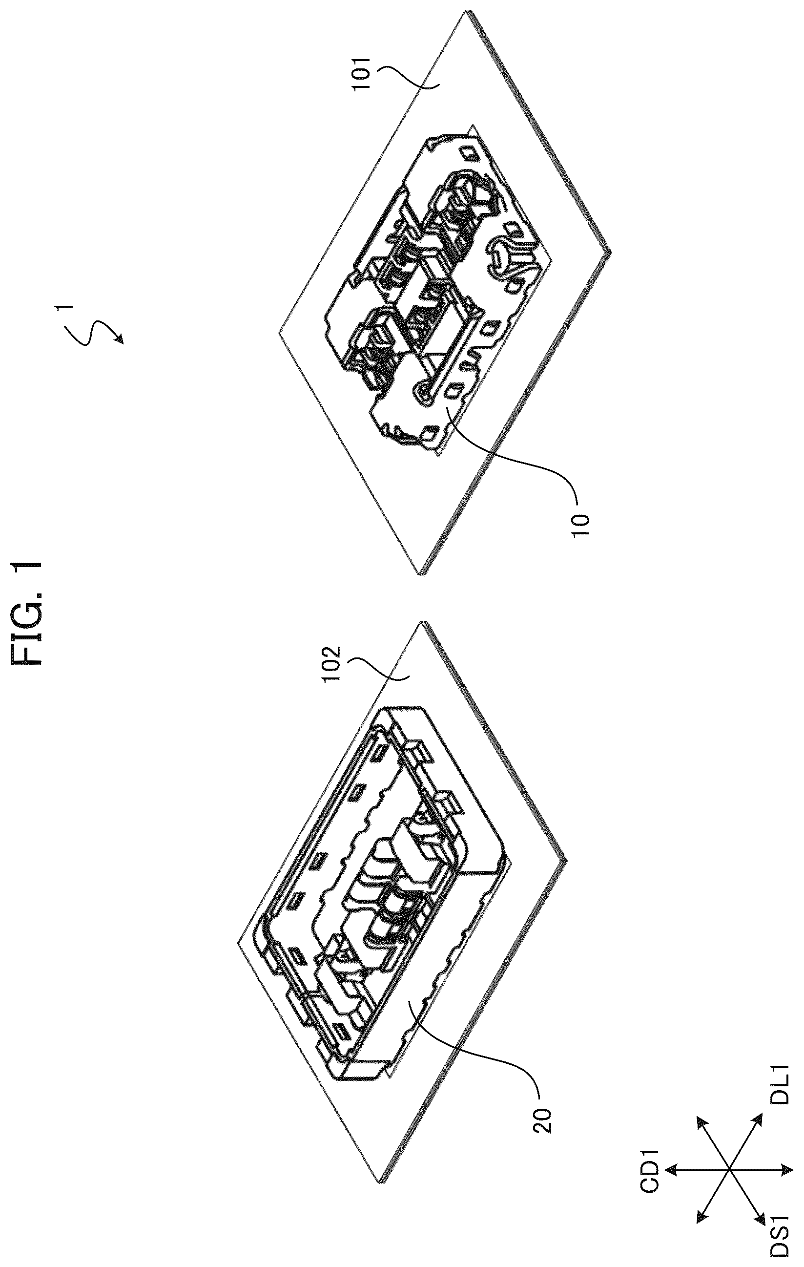
A connector unit 1 is a unit that is used to connect circuit boards in an electronic device. Specific examples of the electronic device include portable communication terminals such as mobile phones, smartphones, laptop computers, and tablet computers, but the electronic device is not limited thereto. As illustrated in , the connector unit 1 includes a receptacle connector 10 and a plug connector 20 . A circuit board 101 and a circuit board 102 are electrically connected by fitting the receptacle connector 10 and the plug connector 20 together.
In a state in which the receptacle connector 10 and the plug connector 20 are disposed (placed) so as to fit together, the shape of the plug connector 20 when viewed from the receptacle connector 10 and the shape of the receptacle connector 10 when viewed from the plug connector 20 are both similar to rectangles. Additionally, in the state in which the receptacle connector 10 and the plug connector 20 are disposed so as to fit together, a long side direction (longitudinal direction) of the receptacle connector 10 and a long side direction (longitudinal direction) of the plug connector 20 are substantially parallel to each other. A short side direction (lateral direction) of the receptacle connector 10 and a short side direction (lateral direction) of the plug connector 20 are substantially parallel to each other. Moreover, the lateral directions are substantially at right angles to the longitudinal directions. In the following, a direction along the long sides of this rectangle is referred to as a “long side direction DL 1 ”, and a direction along the short sides of this rectangle is referred to as a “short side direction DS 1 .” A direction perpendicular to this rectangle (normal direction of the circuit board) is referred to as a “connecting direction CD 1 ” of the receptacle connector 10 and the plug connector 20 . In the following, when describing the structure of the plug connector 20 viewed from the receptacle connector 10 in the state in which the receptacle connector 10 and the plug connector 20 are disposed so as to fit together, the phrase “viewed from the receptacle connector 10 ” is simply used. When describing the structure of the receptacle connector 10 viewed from the plug connector 20 , the phrase “viewed from the plug connector 20 ” is simply used. Additionally, in the various drawings, each member is denoted with a reference numeral and, when a larger constituent that includes the member is denoted with a reference numeral, the reference numeral of the larger constituent is denoted in parentheses.
Receptacle Connector
Firstly, the configuration of the receptacle connector 10 is described. As illustrated in , the receptacle connector 10 is attached to the circuit board 101 and connects to the plug connector 20 that is the mating connector, thereby enabling communication between a circuit on the circuit board 101 and a circuit on the circuit board 102 . A surface of the receptacle connector 10 that is attached to the circuit board 101 is referred to as a “bottom surface”, and a surface opposite the bottom surface is referred to as a “top surface.” As illustrated in to 4 , the receptacle connector 10 includes a plurality of electrically conductive contacts 4 , a contact holder 5 that holds the contacts 4 , and a shell 6 that covers the contact holder 5 .
Each of the contacts 4 is connected to a conductor (wiring) of the circuit formed on the circuit board 101 , and contacts a corresponding contact 7 (described later) of the plug connector 20 . The contacts 4 are formed by punching a single layer plate material from a metal thin plate, and subjecting the obtained plate material to bending or the like. The plurality of contacts 4 may include contacts 4 of mutually different types. For example, the plurality of contacts 4 includes a plurality of type 1 contacts 4 A, and at least one type 2 contact 4 B of a different type than the type 1 contacts 4 A. In one example, the receptacle connector 10 includes four of the type 1 contacts 4 A and two of the type 2 contacts 4 B.
The phrase “of different types” means belonging to mutually different types based on definitions that identify the types. Specific examples of type differences include a difference in the frequency band of the signal to be transmitted, a difference in allowable current, a difference in allowable voltage, a difference in whether for connecting a signal conductor (a conductor forming a portion of a signal circuit) or for connecting a ground connector (a conductor forming a portion of a ground circuit), and the like. In the following description, an example is given in which the type 2 contacts 4 B are contacts that transmit signals of a higher frequency than the type 1 contacts 4 A.
As illustrated in A that corresponds to a cross-sectional view taken along line WA of B , each of the type 1 contacts 4 A includes a connecting portion 41 A and a contacting portion 42 A. An end of the connecting portion 41 A is connected to a conductor (for example, a signal conductor) of the circuit board 101 . The contacting portion 42 A contacts a contact 7 (described later) of the plug connector 20 . The connecting portion 41 A and the contacting portion 42 A are coupled to each other.
The contacting portion 42 A includes a first portion 421 , a second portion 422 , and a coupling portion 423 . The first portion 421 and the second portion 422 each project (extend) toward the plug connector 20 along the connecting direction CD 1 from a base near the bottom surface of the receptacle connector 10 , and sandwich the contact 7 of the plug connector 20 when the receptacle connector 10 and the plug connector 20 are fitted together. The coupling portion 423 connects the base of the first portion 421 and the base of the second portion 422 . The connecting portion 41 A is bent back and extends toward the bottom surface from a tip of the first portion 421 . An end of the connecting portion 41 A projects outward. Note that the connecting portion 41 A may have any shape provided that attachment to the circuit board 101 is possible, and may have a shape that does not project outward.
As illustrated in B that corresponds to a cross-sectional view taken along line IVB of B , and A to 5 D , the type 2 contacts 4 B each include a connecting portion 41 B, a contacting portion 42 B, and an engaged portion 43 B. The connecting portion 41 B connects a projection 412 forming the bottom (projecting from the bottom) of the base 411 to a conductor (for example, a signal conductor) of the circuit board 101 . The contacting portion 42 B contacts the contact 7 (described later) of the plug connector 20 . The type 2 contact 4 B is fixed to the receptacle connector 10 as a result of the engaged portion 43 B engaging with (an engaging portion of) the contact holder 5 . The connecting portion 41 B, the contacting portion 42 B, and the engaged portion 43 B are formed as an integrated part.
The connecting portion 41 B is a part that contacts the conductor of the circuit board 101 , and is positioned directly below the contacting portion 42 B (near the bottom surface in the connecting direction CD 1 ). The connecting portion 41 B includes a base 411 , and the projection 412 that projects slightly from the bottom of the base 411 . The projection 412 is connected to a conductor (for example, a signal conductor) of the circuit board 101 . A circular hole 413 is provided at the center of the projection 412 and the base 411 . Mounting on the circuit board 101 can be confirmed through the hole 413 . Note that the connecting portion 41 B may have any shape provided that attachment to the circuit board 101 is possible, and may have a structure that does not include the projection 412 .
The contacting portion 42 B is a part that contacts the contact 7 of the plug connector 20 , and includes a first arm 424 and a second arm 425 . The first arm 424 and the second arm 425 each project toward the plug connector 20 along the connecting direction CD 1 from both sides of the base 411 , and sandwich the contact 7 of the plug connector 20 when the receptacle connector 10 and the plug connector 20 are fitted together. Portions near the tips of the first arm 424 and the second arm 425 respectively curve toward the connecting portion 41 B, and form pressers 426 . The first arm 424 and the second arm 425 are formed in a plane symmetrical shape with respect to a DL 1 -CD 1 plane that passes through the base 411 . Note that the directions in which the first arm 424 and the second arm 425 project with respect to the reference plane, namely the DL 1 -CD 1 plane, need not be the same. For example, the first arm 424 may project along a direction inclined toward the connecting direction CD 1 , and the second arm 425 may project opposite the first arm 424 .
The engaged portion 43 B is a part for fixing the type 2 contact 4 B to the contact holder 5 . The engaged portion 43 B includes a first portion 431 and a second portion 432 that extend from both sides of the base 411 in a direction that crosses the extending direction of the contacting portion 42 B. The first portion 431 is formed in a flat plate shape, and a tip thereof includes a substantially trapezoidal protrusion 433 that rises along the connecting direction CD 1 . The protrusion 433 is positioned near a type 1 holding area 51 (described later) of the contact holder 5 . The second portion 432 is formed in a flat plate shape, and is positioned near a surrounding wall 62 (described later) of the contact holder 5 .
The contact holder 5 is an insulating member that holds the plurality of contacts 4 . In one example, the contact holder 5 is formed by injection molding a resin material or the like. As illustrated in , the contact holder 5 includes a bottom surface 55 that opposes the circuit board 101 , a top surface 54 opposite the bottom surface 55 , a type 1 contact holder that holds the type 1 contacts 4 A, and a type 2 contact holder that holds the type 2 contacts 4 B. Viewed from the plug connector 20 , the contact holder 5 has an outer shape similar to a rectangle. This rectangle includes a pair of long sides 5 a and 5 b arranged along the long side direction DL 1 , and a pair of short sides 5 c and 5 d arranged along the short side direction DS 1 .
The contact holder 5 is partitioned, in a direction perpendicular to the connecting direction CD 1 , into a plurality of holding areas. In the present embodiment, the plurality of holding areas includes a type 1 holding area 51 partitioned as the type 1 contact holder, and a type 2 holding area 52 partitioned as the type 2 contact holder. The type 1 holding area 51 holds a plurality of the contacts 4 . In one example, the type 1 holding area 51 holds the four type 1 contacts 4 A. The type 2 holding area 52 holds one of the contacts 4 and does not hold the other contacts 4 . In one example, the type 2 holding area 52 holds one of the type 2 contacts 4 B.
The plurality of holding areas may include two of the type 2 holding areas 52 , and at least one type 1 holding area 51 may be interposed among the plurality of type 2 holding areas 52 . In one example, the contact holder 5 is partitioned into one type 1 holding area 51 , and two type 2 holding areas 52 , which sandwich the type 1 holding area 51 . The type 1 holding area 51 and the two type 2 holding areas 52 are arranged in the long side direction DL 1 . In the following, the two type 2 holding areas 52 are distinguished as type 2 holding areas 52 A and 52 B.
The plurality of holding areas may be partitioned by spaces formed in the contact holder 5 . In one example, the type 2 holding area 52 A and the type 1 holding area 51 are partitioned by a space S 11 formed along a boundary PL 11 parallel to the short side direction DS 1 . In the present embodiment, the type 2 holding area 52 A and the type 1 holding area 51 are partitioned by a slit 53 A parallel to the short side direction DS 1 .
The type 1 holding area 51 and the type 2 holding area 52 B are partitioned by a space S 12 formed along a boundary PL 12 parallel to the short side direction DS 1 . In one example, the type 1 holding area 51 and the type 2 holding area 52 B are partitioned by a slit 53 B parallel to the short side direction DS 1 .
Note that, herein, the term “space” does not mean a space in a state in which the receptacle connector 10 is completed, but means a space in a case in which the contact holder 5 exists alone. That is, the term “space” includes portions that are filled in by other members different from the contact holder 5 in the state in which the receptacle connector 10 is completed. For example, at least a portion of the space S 11 is filled in by a partition wall 61 A, described later, and at least a portion of the space S 12 is filled in by a partition wall 61 B, described later.
In the contact holder 5 , the type 2 contacts 4 B disposed in the type 2 holding areas 52 A and 52 B are disposed such that the connecting portion 41 B and the contacting portion 42 B appear to overlap when viewed from the connecting direction CD 1 . In other words, the type 2 contacts 4 B are disposed such that the portions contacting the contacts 7 of the plug connector 20 and the contacting portions 42 B are arranged in the same direction. For example, the type 2 contacts 4 B are disposed such that the positional relationships of the connecting portions 41 B and the contacting portions 42 B are arranged along the connecting direction CD 1 . Viewed from the plug connector 20 , the contacting portions 42 B of the type 2 contacts 4 B are disposed inward from the outer edge of the contact holder 5 .
Viewed from the connecting direction CD 1 , the plurality of type 1 contacts 4 A are disposed in the type 1 holding area 51 such that a coupling direction (direction in which the coupled connecting portion 41 A and contacting portion 42 A are arranged) of the connecting portion 41 A and the contacting portion 42 A of each type 1 contact 4 A is arranged in the same direction. In other words, the type 1 contacts 4 A are disposed such that the portions contacting the contacts 7 of the plug connector 20 and the contacting portions 42 A are arranged in the same direction. For example, the type 1 contacts 4 A are disposed such that the coupling direction between the connecting portion 41 A and the contacting portion 42 A is arranged in the short side direction DS 1 . Viewed from the plug connector 20 , the contacting portions 42 A of the type 1 contacts 4 A are disposed inward from the outer edge of the contact holder 5 .
As illustrated in , each of the type 1 holding area 51 and the type 2 holding areas 52 includes an accommodation groove arranged along the same direction (the long side direction DL 1 in the present embodiment). As illustrated in , in each of the type 1 holding area 51 and the type 2 holding areas 52 , the contacting portions 42 A and 42 B of all of the contacts 4 A and 4 B are disposed so as to be exposed from the accommodation groove. A raised holding portion (described later) of the plug connector 20 is accommodated in the accommodation groove. The contacts 4 A and 4 B are disposed such that the contacting portions 42 A and 42 B contact contacting portions 72 (described later) of the contacts 7 disposed on the plug connector 20 .
One accommodation groove is positioned nearer to the long side 5 a than a center axis C 1 that is arranged along the long side direction DL 1 , and another accommodation groove is positioned nearer to the long side 5 b than the center axis C 1 . The two accommodation grooves are located at line symmetrical positions with respect to the center axis C 1 .
In the present embodiment, as illustrated in , the type 1 holding area 51 includes two accommodation grooves 511 A and 511 B that are parallel to each other. The accommodation grooves 511 A and 511 B are formed on the top surface 54 of the contact holder 5 along the long side direction DL 1 . On the top surface 54 , the accommodation groove 511 A is positioned nearer to the long side 5 a than the center axis C 1 , and the accommodation groove 511 B is positioned nearer to the long side 5 b than the center axis C 1 . The accommodation groove 511 A is located at a position that has line symmetry with the accommodation groove 511 B, with respect to the center axis C 1 that is arranged along the long side direction DL 1 .
As illustrated in , the type 1 contacts 4 A held by the type 1 holding area 51 include two contacts disposed arranged along the accommodation groove 511 A, and two contacts disposed arranged along the accommodation groove 511 B. That is, the type 1 holding area 51 includes a plurality of the type 1 contacts 4 A arranged along the long side direction DL 1 . Here, “a region α sandwiched by the type 1 contacts 4 A that face each other in the short side direction DS 1 ” refers to a region sandwiched by the type 1 contacts 4 A disposed in the accommodation groove 511 A and the type 1 contacts 4 A disposed in the accommodation groove 511 B. Note that “the region α sandwiched by the set of type 1 contacts 4 A” may include from a portion where the type 1 contacts 4 A disposed in the accommodation groove 511 A contact a recess 515 A, described later, to a portion where the type 1 contacts 4 A disposed in the accommodation groove 511 B contact a recess 515 B, described later. Specifically, “the region α sandwiched by the set of type 1 contacts 4 A” may include the region in which the type 1 contacts 4 A accommodated in the accommodation groove 511 A are disposed, and the region in which the type 1 contacts 4 A accommodated in the accommodation groove 511 B are disposed.
In the present embodiment, as illustrated in , the type 1 holding area 51 includes two contact accommodators 512 A arranged along the accommodation groove 511 A. Each of the contact accommodators 512 A includes a hole that penetrates from the bottom surface 55 of the contact holder 5 to the accommodation groove 511 A. The contact accommodators 512 A are located at positions that have line symmetry with a contact accommodator 512 B, described later, with respect to the center axis C 1 . Furthermore, the two contact accommodators 512 A are located at line symmetrical positions with respect to a center axis C 2 therebetween, the center axis C 2 being arranged along the short side direction DS 1 . As illustrated in A , the contacting portion 42 A of each of the type 1 contacts 4 A is fixed in each of the contact accommodators 512 A by press fitting or the like, such that the first portion 421 and the second portion 422 are exposed to the outside from the accommodation groove 511 A. As a result of this configuration, the type 1 contacts 4 A disposed in the accommodation groove 511 A are disposed such that a direction in which a line, that connects the connecting portion 41 A and the contacting portion 42 A, extends when viewed from the connecting direction CD 1 is parallel to the short side direction DS 1 . As illustrated in B , the connecting portion 41 A of each type 1 contact 4 A disposed in the accommodation groove 511 A projects toward the long side 5 a ( 5 b ) from the contacting portion 42 A.
As illustrated in , the type 1 holding area 51 further includes a recess 515 A in a center section (center section in the long side direction DL 1 ) of a side surface arranged along the long side 5 a . The recess 515 A is formed throughout, from the top surface 54 to the bottom surface 55 . As illustrated in A , the connecting portions 41 A of the type 1 contacts 4 A disposed in the accommodation groove 511 A are exposed to the inside of the recess 515 A when viewed from the plug connector 20 . Due to this configuration, connection states of the connecting portions 41 A to the circuit board 101 can be visually confirmed.
Additionally, as illustrated in , the type 1 holding area 51 includes two contact accommodators 512 B arranged along the accommodation groove 511 B. Each of the contact accommodators 512 B includes a hole that penetrates from the bottom surface 55 of the contact holder 5 to the accommodation groove 511 B. The two contact accommodators 512 B are located at line symmetrical positions with respect to the center axis C 2 therebetween, the center axis C 2 being arranged along the short side direction DS 1 . Accordingly, the two contact accommodators 512 A and the two contact accommodators 512 B are disposed having point symmetry with respect to an intersection CP of the center axes C 1 and C 2 . That is, when the contact holder 5 rotates 180° around the intersection CP on the DL 1 -DS 1 plane, the contact accommodators 512 A move to the positions where the contact accommodators 512 B existed, and the contact accommodators 512 B move to the positions where the contact accommodators 512 A existed. As illustrated in A , the contacting portions 42 are fixed in each of the contact accommodators 512 B by press fitting or the like, such that the first portion 421 and the second portion 422 are exposed. As a result of this configuration, each of the type 1 contacts 4 A arranged along the accommodation groove 511 B is disposed such that a direction in which a line, that connects the connecting portion 41 A and the contacting portion 42 A, extends when viewed from the connecting direction CD 1 is parallel to the short side direction DS 1 . As illustrated in B , the connecting portion 41 A of each type 1 contact 4 A disposed in the accommodation groove 511 B projects toward the long side 5 b from the contacting portion 42 A. That is, the connecting portions 41 A of the type 1 contacts 4 A of the accommodation groove 511 A and the connecting portions 41 A of the type 1 contacts 4 A of the accommodation groove 511 B project in mutually opposite directions.
As illustrated in , the type 1 holding area 51 further includes a recess 515 B in a center section (center section in the long side direction DL 1 ) of a side surface arranged along the long side 5 b . As illustrated in A , the connecting portions 41 A of the type 1 contacts 4 A disposed in the accommodation groove 511 B are exposed to the inside of the recess 515 B when viewed from the plug connector 20 .
As illustrated in , each of the type 2 holding areas 52 A and 52 B includes one accommodation groove 521 . The accommodation groove 521 extends parallel to the long side direction DL 1 and is formed on the top surface 54 of the contact holder 5 . On the top surface 54 , the accommodation groove 521 is positioned in the middle between the long side 5 a and the long side 5 b (the middle in the short side direction DS 1 ).
The type 2 contacts 4 B are disposed in each of the accommodation grooves 521 . Additionally, each of the type 2 holding areas 52 A and 52 B includes one contact accommodator 522 . The contact accommodator 522 includes a hole that is provided on the bottom surface 55 of the contact holder 5 and that is open to the accommodation groove 521 . The contacting portions 42 B of the type 2 contacts 4 B are fixed in the accommodation groove 521 by press fitting or the like, such that the first arm 424 and the second arm 425 are exposed. The type 2 contacts 4 B are disposed in the accommodation groove 521 such that a line, that connects the connecting portion 41 B and the contacting portion 42 B, is parallel to the connecting direction CD 1 . The accommodation groove 521 is provided in the region α that is sandwiched between the set of type 1 contacts 4 A in the short side direction DS 1 . Specifically, the accommodation groove 521 is provided on the center axis C 1 . Distances from the two contact accommodators 522 to the center axis C 2 are equivalent. Accordingly, when the contact holder 5 rotates 180° around the intersection CP on a plane parallel to DL 1 and DS 1 , the positions of the two contact accommodators 522 (and the type 2 contacts 4 B) are interchanged.
As illustrated in , the type 2 holding area 52 B further includes a recess 525 on one outer corner portion. The recess 525 is a portion sunken from the top surface 54 toward the bottom surface 55 .
The type 2 contact 4 B held by the type 2 holding area 52 A is adjacent to the type 1 contacts 4 A of the type 1 holding area 51 across a boundary PL 11 . The type 2 contact 4 B held by the type 2 holding area 52 B is adjacent to the type 1 contacts 4 A of the type 1 holding area 51 across a boundary PL 12 . Thus, a gap G 11 in the long side direction DL 1 (the arrangement direction) of the contacts 4 adjacent across the boundaries PL 11 and PL 12 is larger than a gap G 12 of the contacts 4 adjacent along the long side direction DL 1 in the type 1 holding area 51 (see ).
The shell 6 illustrated in is an electrically conductive member that is mounted on the contact holder 5 . As illustrated in , the shell 6 includes at least one partition wall 61 that partitions the contact holder 5 into a plurality of holding areas. The partition wall 61 is electrically connected to a ground conductor (not illustrated in the drawings) of the circuit board 101 . The partition wall 61 may be directly connected to the ground conductor of the circuit board 101 , or may be connected to the ground conductor of the circuit board 101 via another portion of the shell 6 . The shell 6 may include two partition walls 61 that are interposed between the type 2 holding area 52 A and the type 2 holding area 52 B. The at least one type 1 holding area 51 may be interposed between these two partition walls 61 .
In one example, the shell 6 includes partition walls 61 A and 61 B as the two partition walls 61 . The partition wall 61 A is positioned in the space S 11 , and partitions the type 2 holding area 52 A and the type 1 holding area 51 . The partition wall 61 B is positioned in the space S 12 , and partitions the type 1 holding area 51 and the type 2 holding area 52 B. As illustrated in , each of the partition walls 61 A and 61 B includes an end edge 611 (an end) that contacts the circuit board 101 , and is electrically connected to the ground conductor of the circuit board 101 at that end edge 611 .
As illustrated in , the shell 6 may further include an electrically conductive surrounding wall 62 aligned with the partition wall 61 along the outer periphery of the type 2 holding areas 52 . The shell 6 may include a surrounding wall 62 for each of the type 2 holding areas 52 A and 52 B. In one example, the shell 6 includes an electrically conductive surrounding wall 62 A aligned with the partition wall 61 A along the outer periphery of the type 2 holding area 52 A, and an electrically conductive surrounding wall 62 B aligned with the partition wall 61 B along the outer periphery of the type 2 holding area 52 B. Each of the surrounding walls 62 A and 62 B includes an opposing portion 621 and side portions 622 A and 622 B.
The opposing portions 621 oppose the partition walls 61 across the type 2 holding areas 52 . For example, the opposing portion 621 of the surrounding wall 62 A covers at least a portion of the side surface arranged along the short side 5 c of the contact holder 5 , and opposes the partition wall 61 A across the type 2 holding area 52 A. The opposing portion 621 of the surrounding wall 62 B covers at least a portion of the side surface arranged along the short side 5 d of the contact holder 5 , and opposes the partition wall 61 B across the type 2 holding area 52 B. As illustrated in , the opposing portion 621 includes an end edge 625 (an end) that contacts the circuit board 101 , and is electrically connected to the ground conductor of the circuit board 101 at that end edge 625 . The opposing portion 621 includes a protrusion that protrudes outward (direction opposite the direction toward the type 2 holding areas 52 ). For example, as illustrated in , the opposing portion 621 includes two protrusions 623 arranged along the short side direction DS 1 , and press fitters 624 at the middle between the two protrusions 623 . The press fitters 624 are formed by cutting and bending such that the center projects outward.
The side portion 622 A covers at least a portion of the side surface arranged along the long side 5 a of the type 2 holding areas 52 . The side portion 622 B covers at least a portion of the side surface arranged along the long side 5 b of the type 2 holding areas 52 . As illustrated in , each of the side portions 622 A and 622 B includes an end edge (an end) 627 that contacts the circuit board 101 , and is electrically connected to the ground conductor of the circuit board 101 at that end edge 627 . Each of the side portions 622 A and 622 B includes a plurality of protrusions 626 that protrudes outward (direction opposite the direction toward the type 2 holding areas 52 ).
As illustrated in , the shell 6 may further include an electrically conductive in-area connection plate 63 (in-area connecting portion) that electrically connects the partition walls 61 and the surrounding walls 62 that are arranged along the outer peripheries of the type 2 holding areas 52 to each other. The in-area connection plate 63 may expand so as to cross the connecting direction CD 1 . The in-area connection plate 63 may be disposed so as to face the plug connector 20 .
The shell 6 may include an in-area connection plate 63 for each of the type 2 holding areas 52 A and 52 B. In one example, the shell 6 includes in-area connection plates 63 A and 63 B at two locations. The in-area connection plate 63 A electrically connects the partition wall 61 A and the surrounding wall 62 A arranged along the outer periphery of the type 2 holding area 52 A to each other. More specifically, the in-area connection plate 63 A covers at least a portion of the top surface 54 , and is connected to the end edge of the partition wall 61 A, the end edge of the opposing portion 621 of the surrounding wall 62 A, and the end edges of the side portions 622 A and 622 B of the surrounding wall 62 A.
The in-area connection plate 63 B electrically connects the partition wall 61 B and the surrounding wall 62 B arranged along the outer periphery of the type 2 holding area 52 B to each other. More specifically, the in-area connection plate 63 B covers at least a portion of the top surface 54 , and is connected to the end edge of the partition wall 61 B, the end edge of the opposing portion 621 of the surrounding wall 62 B, and the end edges of the side portions 622 A and 622 B of the surrounding wall 62 B. Each of the in-area connection plates 63 A and 63 B includes an opening 631 for exposing the type 2 contacts 4 B disposed in the type 2 holding areas 52 .
As illustrated in , the shell 6 may further include an intra-area connection plate (intra-area connecting portion) 64 that electrically connects the partition wall 61 A of the outer periphery of the type 2 holding area 52 A and the partition wall 61 B of the outer periphery of the type 2 holding area 52 B. The intra-area connection plate 64 may be arranged along the outer periphery of the type 1 holding area 51 . In one example, the shell 6 includes intra-area connection plates 64 A and 64 B.
The intra-area connection plate 64 A covers at least a portion of the side surface arranged along the long side 5 a of the type 1 holding area 51 , and electrically connects the partition wall 61 A and the partition wall 61 B. Due to this configuration, the two type 1 contacts 4 A in the accommodation groove 511 A are arranged along the intra-area connection plate 64 A and are disposed such that each of the connecting portions 41 A projects toward the intra-area connection plate 64 A. The intra-area connection plate 64 A opposes the connecting portions 41 A of the two type 1 contacts 4 A.
The intra-area connection plate 64 B covers at least a portion of the side surface arranged along the long side 5 b of the type 1 holding area 51 , and electrically connects the partition wall 61 A and the partition wall 61 B. Due to this configuration, the two type 1 contacts 4 A in the accommodation groove 511 B are arranged along the intra-area connection plate 64 B and are disposed such that each of the connecting portions 41 A projects toward the intra-area connection plate 64 B. The intra-area connection plate 64 B opposes the connecting portions 41 A of the two type 1 contacts 4 A.
In the connecting direction CD 1 , as illustrated in , the intra-area connection plates 64 A and 64 B each include an end edge 642 that opposes the circuit board 101 , and a projection 641 that projects downward from the end edge 642 and that contacts a shell 8 , described later, of the plug connector 20 . The projection 641 is positioned in the middle between the partition walls 61 A and 61 B (middle of the long side direction DL 1 ). The projection 641 projects outward (direction opposite the direction toward the type 1 holding area 51 ) in order to avoid contact with the connecting portions 41 A of the type 1 contacts 4 A.
Due to the shell 6 including the intra-area connection plates 64 A and 64 B, the type 1 holding area 51 is surrounded by the partition walls 61 A and 61 B and the intra-area connection plates 64 A and 64 B. Additionally, the entire contact holder 5 is surrounded by the surrounding walls 62 A and 62 B and the intra-area connection plates 64 A and 64 B.
In one example, the shell 6 is formed by punching a single layer plate material from a metal thin plate material, and subjecting the obtained plate material to bending or the like. This plate material includes outer walls 691 A, 691 B, 692 A, and 692 B, top plates 695 A and 695 B, and inner walls 696 A and 696 B (see ).
The outer wall 691 A is a plate-like member that forms the side portion 622 A of the surrounding wall 62 A, the side portion 622 A of the surrounding wall 62 B, and the intra-area connection plate 64 A. The outer wall 691 B is a plate-like member that forms the side portion 622 B of the surrounding wall 62 A, the side portion 622 B of the surrounding wall 62 B, and the intra-area connection plate 64 B. The outer wall 692 A is a plate-like member that forms the opposing portion 621 of the surrounding wall 62 A. The outer wall 692 B is a plate-like member that forms the opposing portion 621 of the surrounding wall 62 B. The top plate 695 A is a plate-like member that forms the in-area connection plate 63 A. The top plate 695 B is a plate-like member that forms the in-area connection plate 63 B. The inner wall 696 A is a plate-like member that forms the partition wall 61 A. The inner wall 696 B is a plate-like member that forms the partition wall 61 B.
The shell 6 is formed by bending the outer walls 691 A, 691 B, 692 A, and 692 B and the inner walls 696 A and 696 B in the same direction at about 90 degrees with respect to the top plates 695 A and 695 B. The obtained shell 6 is mounted on the contact holder 5 by press-fitting, for example.
The receptacle connector 10 configured as described above is attached to the circuit board 101 with the bottom surface 55 facing the circuit board 101 . As illustrated in , the circuit board 101 includes ground conductor exposers 111 , 112 , 113 , and 114 , and signal conductor exposers 121 , 122 , 123 , 124 , 125 , and 126 . The ground conductor exposers 111 , 112 , 113 , and 114 are portions where the ground conductor of the circuit board 101 is exposed. The end edge 611 of the partition wall 61 A, the end edge 611 of the partition wall 61 B, the end edges 625 and 627 of the surrounding wall 62 A, and the end edges 625 and 627 of the surrounding wall 62 B are respectively connected to the ground conductor exposers 111 , 112 , 113 , and 114 by solder or the like.
The signal conductor exposers 121 , 122 , 123 , 124 , 125 , and 126 are portions where the six signal conductors of the circuit board 101 are respectively exposed. The connecting portions 41 A of the four type 1 contacts 4 A and the connecting portions 41 B of the two type 2 contacts 4 B are respectively connected to the signal conductor exposers 121 , 122 , 123 , 124 , 125 , and 126 by solder or the like. The signal conductor exposers 125 and 126 are disposed directly below the connecting portions 41 A and 41 B. Note that sizes of the signal conductor exposers 121 , 122 , 123 , and 124 need not necessarily be the same as the sizes of the connecting portions 41 A of the type 1 contacts 4 A. Likewise, sizes of the signal conductor exposers 125 and 126 need not be the same as the sizes of the connecting portions 41 B of the type 2 contacts 4 B. For example, the signal conductor exposers may be larger than the connecting portions. In other words, it is sufficient that the signal conductor exposers are large enough to allow soldering to the connecting portions to be performed (the connecting portions overlap the signal conductor exposers) when attaching the receptacle connector 10 to the circuit board 101 .
Note that the configurations described above are merely examples and may be modified, as appropriate. For example, configurations are possible in which the contact holder 5 is partitioned into four or more holding areas.
Plug Connector
Next, the configuration of the plug connector 20 is described in detail. As described above, the plug connector 20 is attached to a circuit board 102 , and connects to the receptacle connector 10 that is the mating connector. As illustrated in to 11 , the plug connector 20 includes a plurality of contacts 7 , a shell 8 , and a contact holder 9 .
The plurality of contacts 7 are respectively electrically connected to a plurality of conductors of the circuit board 102 , and respectively contact the plurality of contacts 4 of the receptacle connector 10 . The contacts 7 are formed by punching a single layer plate material from a metal thin plate, and subjecting the obtained plate material to bending or the like. The plurality of contacts 7 may include contacts 7 of mutually different types. For example, the plurality of contacts 7 includes a plurality of type 1 contacts 7 A, and at least one type 2 contact 7 B of a different type than the type 1 contacts 7 A. In one example, in , the plug connector 20 includes six of the contacts 7 , and the six contacts 7 include four of the type 1 contacts 7 A and two of the type 2 contacts 7 B. In one example, the type 2 contacts 7 B are contacts that transmit signals of a higher frequency than the type 1 contacts 7 A. The four type 1 contacts 7 A and the two type 2 contacts 7 B are disposed at positions corresponding to the four type 1 contacts 4 A and the two type 2 contacts 4 B that the four type 1 contacts 7 A and the two type 2 contacts 7 B respectively contact.
As illustrated in A that corresponds to a cross-sectional view taken along line XIA of , the type 1 contacts 7 A each include a connecting portion 71 A and a contacting portion 72 A. A conductor (for example a signal conductor) of the circuit board 102 is connected to the connecting portion 71 A. The contacting portion 72 A contacts the contact 4 ( 4 A) of the receptacle connector 10 . The connecting portion 71 A and the contacting portion 72 A are coupled to each other.
The contacting portion 72 A includes a first portion 721 , a second portion 722 , and coupling portions 723 and 724 . The first portion 721 and the second portion 722 are each arranged along the connecting direction CD 1 , and project toward the receptacle connector 10 from a base near the bottom surface of the plug connector 20 . The first portion 721 and the second portion 722 are sandwiched by the first portion 421 and the second portion 422 of the contact 4 A when the receptacle connector 10 and the plug connector 20 are fitted together. For example, the first portion 721 contacts the first portion 421 , and the second portion 722 contacts the second portion 422 . A configuration is possible in which the first portion 721 contacts the second portion 422 , and the second portion 722 contacts the first portion 421 .
The coupling portion 723 couples a tip of the first portion 721 and a tip of the second portion 722 . The coupling portion 724 couples a base of the second portion 722 and the connecting portion 71 . The coupling portion 724 extends along a plane perpendicular to the connecting direction CD 1 from the base of the second portion 722 to the first portion 721 , and is connected to the connecting portion 71 . The connecting portion 71 projects outward from an outer surface (surface facing opposite the second portion 722 ) of the first portion 721 along an extended line of the coupling portion 724 . Note that the connecting portion 71 may have any shape provided that attachment to the circuit board 102 is possible, and may have a shape that does not project outward.
As illustrated in B that corresponds to a cross-sectional view taken along line XIB of , and A and 12 B , the type 2 contacts 7 B each include a connecting portion 71 B and a contacting portion 72 B. A conductor (for example a signal conductor) of the circuit board 102 is connected to the connecting portion 71 B. The contacting portion 72 B contacts the contact 4 ( 4 B) of the receptacle connector 10 . The connecting portion 71 B and the contacting portion 72 B are coupled to each other.
The contacting portion 72 B is disposed at a position separated from the connecting portion 71 B in the connecting direction CD 1 , which is the normal direction of the installation surface to the circuit board 101 . The contacting portion 72 B includes a first portion 721 , a second portion 722 , and a coupling portion 723 B. The first portion 721 and the second portion 722 extend from the connecting portion 71 B along the connecting direction CD 1 toward the receptacle connector 10 , in a state in which back surfaces of the first portion 721 and the second portion 722 are in contact with each other. The first portion 721 and the second portion 722 are sandwiched by the first arm 424 and the second arm 425 of the contact 4 B when the receptacle connector 10 and the plug connector 20 are fitted together. For example, between the first arm 424 and the second arm 425 , the first portion 721 contacts the first arm 424 , and the second portion 722 contacts the second arm 425 . A configuration is possible in which the first portion 721 contacts the second arm 425 , and the second portion 722 contacts the first arm 424 .
The coupling portion 723 B couples a tip of the first portion 721 and a tip of the second portion 722 . One connecting portion 71 B extends from the base of the first portion 721 toward a side wall 81 A of the shell 8 , described later, and the other connecting portion 71 B extends from the base of the second portion 722 toward a side wall 81 B of the shell 8 , described later. Note that the connecting portion 71 B may have any shape provided that connection to the circuit board 102 is possible.
The shell 8 is an electrically conductive member that surrounds the plurality of contacts 7 . As illustrated in , when viewed from the receptacle connector 10 , the shell 8 surrounds a region having an outer shape similar to a rectangle. This rectangle includes a pair of long sides 8 a and 8 b arranged along the long side direction DL 1 , and a pair of short sides 8 c and 8 d arranged along the short side direction DS 1 . The shell 8 includes a side wall 81 A arranged along the long side 8 a , a side wall 81 B arranged along the long side 8 b , a side wall 82 A arranged along the short side 8 c , and a side wall 82 B arranged along the short side 8 d.
As illustrated in , in a state in which the plug connector 20 and the receptacle connector 10 are fitted together, the shell 8 is positioned on an outer periphery of the shell 6 . In this state, the side wall 81 A of the shell 8 contacts the side portion 622 A of the surrounding wall 62 A, the side portion 622 A of the surrounding wall 62 B, and the intra-area connection plate 64 A of the shell 6 . Additionally, the side wall 81 B of the shell 8 contacts the side portion 622 B of the surrounding wall 62 A, the side portion 622 B of the surrounding wall 62 B, and the intra-area connection plate 64 B of the shell 6 . Moreover, the side wall 82 A of the shell 8 illustrated in contacts the opposing portion 621 of the surrounding wall 62 A of the shell 6 illustrated in . The side wall 82 B of the shell 8 illustrated in contacts the opposing portion 621 of the surrounding wall 62 B of the shell 6 illustrated in .
As illustrated in , the side wall 81 B of the shell 8 includes four recesses 811 on an inner surface (surface opposing the side wall 81 A). Likewise, the side wall 81 A includes four non-illustrated recesses 811 on an inner surface (surface opposing the side wall 81 B). The recesses 811 respectively engage with the protrusions 626 of the surrounding wall 62 A and the surrounding wall 62 B of the shell 6 .
As illustrated in , each of the side walls 81 A and 81 B includes an end edge 813 that opposes the circuit board 102 , and a ground connecting portion 815 at least one location that projects from the end edge 813 and contacts the circuit board 102 . For example, each of the side walls 81 A and 81 B includes three ground connecting portions 815 arranged in the long side direction DL 1 . Each of the side walls 81 A and 81 B is electrically connected to the ground conductor of the circuit board 102 at the ground connecting portions 815 .
As illustrated in A and 11 B , the side wall 82 A includes a recess 821 at two locations of an inner surface (surface opposing the side wall 82 B). These recesses 821 respectively engage with the two protrusions 623 of the surrounding wall 62 A of the shell 6 illustrated in . Furthermore, the side wall 82 A includes a press fitted portion 822 at a middle position between the recesses 821 and 821 of the inner surface. The press fitter 624 of the surrounding wall 62 A is press-fitted into the press fitted portion 822 . Likewise, the side wall 82 B includes two non-illustrated recesses 821 on an inner surface (surface opposing the side wall 82 A). These two recesses 821 engage with the two protrusions 623 of the surrounding wall 62 B. Additionally, the side wall 82 B includes the press fitted portion 822 at a middle position between the recesses 821 and 821 of the inner surface. The press fitter 624 of the surrounding wall 62 B is press-fitted into the press fitted portion 822 .
As illustrated in , each of the side walls 82 A and 82 B includes an end edge 823 that opposes the circuit board 102 , and a ground connecting portion 825 at at least one location that projects from the end edge 823 and contacts the circuit board 102 . For example, each of the side walls 82 A and 82 B includes a ground connecting portion 825 at two locations arranged along the short side direction DS 1 . Each of the side walls 82 A and 82 B is electrically connected to the ground conductor of the circuit board 102 at the ground connecting portions 825 .
As illustrated in , the shell 8 is divided into two shell members 80 A and 80 B that are arranged in the short side direction DS 1 at a middle section (for example, between the two locations of ground connecting portions 825 ) in the short side direction DS 1 of the side wall 82 A, and a middle section (for example, between the two locations of ground connecting portions 825 ) in the short side direction DS 1 of the side wall 82 B. The shell member 80 A includes the side wall 81 B, and the shell member 80 B includes the side wall 81 A.
In one example, each of the shell members 80 A and 80 B is formed by punching a single layer plate material from a metal thin plate material, and subjecting the obtained plate material to bending or the like. By forming the shell 8 from two members in this manner, ease of machining can be realized. Note that a configuration is possible in which, for example, the shell 8 is formed by punching a single layer plate material from a metal thin plate material, and subjecting the obtained plate material to bending or the like.
The contact holder 9 illustrated in is an insulating member that holds the plurality of contacts 7 and the shell 8 . In one example, the contact holder 9 is formed by insert molding in a state in which the plurality of contacts 7 and the shell 8 are disposed.
As illustrated in , the contact holder 9 includes a frame 93 and a main body 94 . The frame 93 holds at least a portion (for example, the side walls 82 A and 82 B) of the shell 8 from the outer periphery side. The main body 94 is disposed between the side walls 82 A and 82 B, and is coupled to the frame 93 . As illustrated in , the main body 94 includes a bottom surface 96 that faces the circuit board 102 , and a top surface 95 opposite the bottom surface 96 (see ). As illustrated in , the main body 94 is partitioned into a plurality of holding areas on the DS 1 -DL 1 plane.
The plurality of holding areas includes a type 1 holding area 91 and a type 2 holding area 92 . The type 1 holding area 91 holds a plurality of the contacts 7 . For example, in , the type 1 holding area 91 holds four of the type 1 contacts 7 A, and each type 2 holding area 92 holds one contact 7 and does not hold other contacts. In one example, the type 2 holding area 92 holds only one type 2 contact 7 B.
The plurality of holding areas may include two type 2 holding areas 92 . At least one type 1 holding area 91 may be interposed among the plurality of type 2 holding areas 92 . In one example, in , the main body 94 is partitioned into one type 1 holding area 91 , and two type 2 holding areas 92 that sandwich the type 1 holding area 91 . The type 1 holding area 91 and the two type 2 holding areas 92 are arranged along the long side direction DL 1 . In the following, the two type 2 holding areas 92 are distinguished as type 2 holding areas 92 A and 92 B.
The plurality of holding areas may be partitioned by spaces formed in the main body 94 . In one example, in , the type 2 holding area 92 A and the type 1 holding area 91 are partitioned by a space S 21 formed along a boundary PL 21 parallel to the short side direction DS 1 . The type 1 holding area 91 and the type 2 holding area 92 B are partitioned by a space S 22 formed along a boundary PL 22 parallel to the short side direction DS 1 .
Note that the spaces need not penetrate the main body 94 along the connecting direction CD 1 , and it is sufficient that at least portions in the connecting direction CD 1 are spaces. In one example, the space S 21 is formed, between a raised holding portion 921 (described later) of the type 2 holding area 92 A and raised holding portions 911 A and 911 B (described later) of the type 1 holding area 91 , in a manner penetrating a portion of the main body 94 and not penetrating the other portion. Additionally, the space S 22 is formed, between raised holding portions 911 A and 911 B (described later) of the type 1 holding area 91 and a raised holding portion 921 (described later) of the type 2 holding area 92 B, in a manner penetrating a portion of the main body 94 and not penetrating the other portion.
As illustrated in A , when viewed from the connecting direction CD 1 , in the contact holder 9 , the type 1 contacts 7 A are disposed such that portions coupling the connecting portions 71 A and the contacting portions 72 A (the directions in which the mutually coupled connecting portions 71 A and contacting portions 72 A are arranged) are arranged in the same direction. In other words, the type 1 contacts 7 A are disposed such that the portions where the contacting portions 72 A and the contacts 4 of the receptacle connector 10 contact each other are arranged in the same direction. In one example, the contacting portions 72 A are disposed such that the portions coupling the connecting portions 71 A and the contacting portions 72 A are aligned with the short side direction DS 1 . When viewed from the receptacle connector 10 , the contacting portions 72 A of all of the contacts 7 A are disposed inward from the outer edge of the contact holder 9 .
As illustrated in , the type 1 holding area 91 and the type 2 holding areas 92 include raised holding portions that extend along the same direction (for example, the long side direction DL 1 ) and that project from the bottom toward the receptacle connector 10 . In each of the type 1 holding area 91 and the type 2 holding areas 92 , the contacting portions 72 of all of the contacts 7 are exposed to a side surface of the raised holding portion.
In one example, as illustrated in , the type 1 holding area 91 includes two raised holding portions 911 A and 911 B that are parallel to each other. The raised holding portions 911 A and 911 B are formed on the main body 94 , extend along the long side direction DL 1 , and project from the top surface (the base) 95 toward the receptacle connector 10 . The raised holding portion 911 A is positioned near the long side 8 a of the shell 8 , and the raised holding portion 911 B is positioned near the long side 8 b of the shell 8 .
The four type 1 contacts 7 A held by the type 1 holding area 91 include two type 1 contacts 7 A arranged along the raised holding portion 911 A, and two type 1 contacts 7 A arranged along the raised holding portion 911 B. That is, the plurality of type 1 contacts 7 A held by the type 1 holding area 91 includes a plurality of type 1 contacts 7 A arranged in the long side direction DL 1 (arrangement direction perpendicular to the boundaries PL 21 and PL 22 ).
Additionally, as illustrated in A , the type 1 contacts 7 A arranged along the raised holding portion 911 A are mounted on the raised holding portion 911 A such that the first portions 721 and the second portions 722 are exposed. As a result of this configuration, each of the type 1 contacts 7 A arranged along the raised holding portion 911 A is disposed such that, when viewed from the connecting direction CD 1 , the coupling direction of the connecting portion 71 A and the contacting portion 72 A is aligned with the short side direction DS 1 . The second portions 722 of the type 1 contacts 7 A penetrate the type 1 holding area 91 from the top surface 95 to the bottom surface 96 , and the coupling portions 724 are exposed to the bottom surface 96 . The connecting portions 71 A project from the coupling portions 724 toward the long side 8 a . When viewed from the receptacle connector 10 , the connecting portions 71 A are exposed between the main body 94 and the long side 8 a . Due to this configuration, the connection states of the connecting portions 71 A to the circuit board 102 can be visually confirmed.
Additionally, as illustrated in A , each of the type 1 contacts 7 A arranged along the raised holding portion 911 B is mounted on the raised holding portion 911 B such that the first portion 721 and the second portion 722 are exposed. As a result of this configuration, each of the type 1 contacts 7 A arranged along the raised holding portion 911 B is disposed such that, when viewed from the connecting direction CD 1 , the coupling direction of the connecting portion 71 A and the contacting portion 72 A is aligned with the short side direction DS 1 . The second portions 722 penetrate the type 1 holding area 91 from the top surface 95 to the bottom surface 96 , and the coupling portions 724 are exposed to the bottom surface 96 . The connecting portions 71 A project from the coupling portions 724 toward the long side 8 b . When viewed from the receptacle connector 10 , the connecting portions 71 A are exposed between the main body 94 and the long side 8 b . Due to this configuration, the connection states of the connecting portions 71 A to the circuit board 102 can be visually confirmed.
In the state in which the plug connector 20 and the receptacle connector 10 are fitted together, as illustrated in , the raised holding portion 911 A is accommodated in the accommodation groove 511 A, and the raised holding portion 911 B is accommodated in the accommodation groove 511 B. In each of the raised holding portions 911 A and 911 B, the first portion 721 of the type 1 contact 7 A contacts the first portion 421 of the type 1 contact 4 A, and the second portion 722 of the type 1 contact 7 A contacts the second portion 422 of the type 1 contact 4 A.
As illustrated in , the type 2 holding areas 92 A and 92 B each include one raised holding portion 921 . The raised holding portion 921 is formed on the top surface 95 of the main body 94 , is formed along the long side direction DL 1 , and projects from the bottom surface toward the receptacle connector 10 . The raised holding portion 921 is positioned in the middle in the short side direction DS 1 , between the long side 8 a and the long side 8 b.
The raised holding portion 921 of the type 2 holding area 92 A is partitioned into raised holding portions 911 A and 911 B of the type 1 holding area 91 by the space S 21 arranged along the boundary PL 21 . The raised holding portion 921 of the type 2 holding area 92 B is partitioned into raised holding portions 911 A and 911 B of the type 1 holding area 91 by the space S 22 arranged along the boundary PL 22 . The one type 2 contact 7 B held by each of the type 2 holding areas 92 A and 92 B is disposed on the raised holding portion 921 .
The type 2 contact 7 B held by the type 2 holding area 92 A is adjacent to the type 1 contacts 7 A of the type 1 holding area 91 across the boundary PL 21 . The type 2 contact 7 B held by the type 2 holding area 92 B is adjacent to the type 1 contacts 7 A of the type 1 holding area 91 across the boundary PL 22 .
As illustrated in , a gap G 21 in the long side direction DL 1 (the arrangement direction) of the contacts 7 adjacent across the boundaries PL 21 and PL 22 is larger than a gap G 22 of the contacts 7 adjacent along the long side direction DL 1 in the type 1 holding area 91 .
As illustrated in , in the state in which the plug connector 20 and the receptacle connector 10 are fitted together, the raised holding portions 921 are accommodated in the accommodation grooves 521 . The first portions 721 of the type 2 contacts 7 B contact the first arms 424 of the type 2 contacts 4 B, and the second portions 722 of the type 2 contacts 7 B contact the second arms 425 of the type 2 contacts 4 B.
The plug connector 20 configured as described above is attached to the circuit board 102 with the bottom surface 96 facing the circuit board 102 . As illustrated in , the circuit board 102 includes a ground conductor exposer 131 , and signal conductor exposers 141 , 142 , 143 , 144 , 145 , and 146 .
The ground conductor exposer 131 is a portion where the ground conductor of the circuit board 102 is exposed. The ground connecting portions 815 at three locations of the side wall 81 A, the ground connecting portions 815 at three locations of the side wall 81 B, the ground connecting portions 825 at two locations of the side wall 82 A, and the ground connecting portions 825 at two locations of the side wall 82 B are connected to the ground conductor exposer 131 by solder or the like.
The signal conductor exposers 141 , 142 , 143 , 144 , 145 , and 146 are portions where the signal conductors of the circuit board 102 are exposed. The connecting portions 71 A of the four type 1 contacts 7 A and the connecting portions 71 B of the two type 2 contacts 7 B are respectively connected to the signal conductor exposers 141 , 142 , 143 , 144 , 145 , and 146 by solder or the like.
As described above, with the receptacle connector 10 and the plug connector 20 , the type 1 contacts 4 A and 7 A and the type 2 contacts 4 B and 7 B are respectively disposed having line symmetry with respect to the center lines C 1 and C 2 (that is, having point symmetry with respect to the point CP). Furthermore, the contacting portions 42 B and 72 B of the type 2 contacts 4 B and 7 B contact the type 2 contacts 7 B and 4 B of the mating connector at positions separated from the connecting portions 41 B and 71 B in the normal direction of the bottom surfaces facing the circuit boards 101 and 102 . As such, even when the orientations of the receptacle connector 10 and the plug connector 20 are reversed, the contact positions of the type 1 contacts 4 A and 7 A and the type 2 contacts 4 B and 7 B do not change from before to after the reversal. Accordingly, the plug connector 20 can be rotated 180° on a plane parallel to the receptacle connector 10 and be fitted together with the receptacle connector 10 .
Therefore, even when reverse mounted, the contact positions of the type 2 contacts 4 B and 7 B do not change from before to after the reversal. Accordingly, the receptacle connector 10 can be reverse mounted on the circuit board 101 . Also, the plug connector 20 can be reverse mounted on the circuit board 102 .
The first portions 431 and the second portions 432 of the type 2 contacts 4 B engage with the contact holder 5 . Accordingly, effects on the connection state between the connecting portions 41 B and the circuit board 101 can be suppressed, even when the plug connector 20 is repeatedly attached and detached.
The type 2 contacts 4 B and 7 B are disposed in the type 2 holding areas 52 and 92 that differ from the type 1 holding areas 51 and 91 in which the type 1 contacts 4 A and 7 A are disposed. As a result, crosstalk noise can be suppressed.
For example, a configuration is possible in which the type 2 contacts 4 B and 7 B are contacts that transmit signals of frequencies higher than those of the signals that the type 1 contacts 4 A and 4 B transmit. Crosstalk noise can be suppressed in this case as well due to the contacts 4 B and 7 B that transfer the high-frequency signals being disposed in the type 2 holding areas 52 A, 52 B, 92 A, and 92 B, separated from the other contacts 4 A and 7 A.
In the present embodiment, the type 1 holding area 51 and the two type 2 holding areas 52 A and 52 B are partitioned by the spaces S 11 and S 12 . Additionally, the type 1 holding area 91 , and the two type 2 holding areas 92 A and 92 B that sandwich the type 1 holding area 91 are partitioned by the spaces S 21 and S 22 . Accordingly, as described above, crosstalk noise can be suppressed. Furthermore, in this case, noise can be more reliably suppressed due to the disposal of electrically conductive members such as the shell 6 , for example, in the spaces S 11 , S 12 , S 21 , and S 22 .
Embodiment 2
A connector unit 2 according to Embodiment 2 differs from the connector unit 1 of Embodiment 1 in that, instead of the receptacle connector 10 including the type 2 contact 4 B, a receptacle connector 11 that includes a type 2 contact 4 B 1 is used.
As illustrated in A to 18 C , the type 2 contact 4 B 1 includes a connecting portion 41 B 1 , a contacting portion 42 B 1 , and an engaged portion 43 B 1 .
The connecting portion 41 B 1 includes a base 411 B 1 connected to a conductor of the circuit board 101 , and two communicating portions 412 B 1 that extend in a direction orthogonal to a direction in which the base 411 B 1 extends. When viewed from above, the base 411 B 1 is formed in a substantially rectangular plate-like shape, and a long axis of the base 411 B 1 is disposed in a direction in which an exposed conductor portion of the circuit board 101 extends. The engaged portion 43 B 1 is provided at the end of each communicating portion 412 B 1 .
A contacting portion 42 B 1 is formed in a line symmetrical shape with respect to a center axis C 11 . The contacting portion 42 B 1 includes springs 421 B 1 , sandwichers 422 B 1 , and guiders 423 B 1 . The springs 421 B 1 extend so as to rise from the communicating portion 412 B 1 in the connecting direction CD 1 , straddling the base 411 B 1 and the exposed conductor portion of the connected circuit board 101 . The pair of sandwichers 422 B 1 extend, in directions that separate from each other, from the springs 421 B 1 toward the plug connector 20 , and then extend so as to approach each other. The pair of guiders 423 B 1 extend, in directions that separate from each other, from the sandwichers 422 B 1 toward the plug connector 20 . The contacting portions 42 B 1 are formed such that a width decreases with proximity to the guiders 423 B 1 . As illustrated in , the sandwichers 422 B 1 sandwich the contact 7 of the plug connector 20 when the receptacle connector 11 and the plug connector 20 are fitted together.
The engaged portion 43 B 1 includes a first portion 431 B 1 and a second portion 432 B 1 . The first portion 431 B 1 includes a substantially T-shaped protrusion 433 B 1 that rises along the connecting direction CD 1 . The second portion 432 B 1 includes a portion extending in a substantial T shape.
As illustrated in , the substantially T-shaped protrusion 433 B 1 of the first portion 431 B 1 is engaged near the type 1 holding area 51 of the contact holder 5 . The second portion 432 B 1 is disposed such that the T-shaped portion is near the surrounding wall 62 of the shell 6 , and causes the substantially T-shaped portion to engage with the contact holder 5 .
Thus, according to the present embodiment, the type 2 contacts 4 B 1 and 7 B each are disposed on the center line C 1 of the type 1 contacts 4 A and 7 A in the lateral direction of each connector and, also, the contacting portions 42 B 1 of the type 2 contacts 4 B 1 and 7 B contact the type 2 contacts 7 B and 4 B 1 of the mating connector at positions separated, in the normal direction of the bottom surfaces that contact the circuit boards 101 and 102 , from the connecting portions 41 B 1 and 71 B. As such, even when reverse mounted, the contact positions of the type 2 contacts 4 B 1 and 7 B do not change from before to after the reversal. Therefore, the receptacle connector 11 can be reverse mounted on the circuit board 101 . Also, the plug connector 20 can be reverse mounted on the circuit board 102 . The springs 421 B 1 of the type 2 contacts 4 B 1 are formed so as to rise from the communicating portion 412 B 1 , straddling the base 411 B 1 and the exposed conductor portion of the connected circuit board 101 . As such, the solder or the like used to connect the base 411 B to the exposed conductor portion can be prevented from obstructing the operations of the springs 421 B 1 . Additionally, the long side of the connecting portion 41 B 1 is disposed overlapping the exposed conductor portion of the circuit board 101 . As such, the connection between the connecting portion 41 B 1 and the circuit board 101 can be made more reliably, and signals can be stably sent and received.
Embodiment 3
A connector unit 3 according to Embodiment 3 differs from the connector unit 1 of Embodiment 1 in that, instead of the receptacle connector 10 , a receptacle connector 12 that includes a type 2 contact 4 B 2 is used.
As illustrated in A and 21 B , the type 2 contact 4 B 2 includes a connecting portion 41 B 2 , a base 42 B 2 , and contacting portions 43 B 2 .
The connecting portion 41 B 2 is formed in a substantially rectangular plate-like shape. The long side of the connecting portion 41 B 2 is disposed in a direction in which an exposed conductor portion of the circuit board 101 extends.
The base 42 B 2 includes a main body 421 B 2 , and an engaged portion 422 B 2 . The main body 421 B 2 is a substantially rectangular plate-like body that rises along the connecting direction CD 1 from an end of the connecting portion 41 B 2 . The engaged portion 422 B 2 is a substantially T-shaped plate-like body that is formed on an end of the main body 421 B 2 . The base 42 B 2 is disposed and engaged near the type 1 holding area 51 of the contact holder 5 .
The contacting portions 43 B 2 are formed in a line symmetrical shape with respect to the connecting portion 41 B 2 . Each of the contacting portions 43 B 2 includes a vertical portion 431 B 2 and a sandwicher 432 B 2 .
The vertical portions 431 B 2 extend bending, from both sides of the main body 421 B 2 , in a direction orthogonal to the main body 421 B 2 and then in the connecting direction CD 1 and, when viewed from the side, are substantially L-shaped or reverse L-shaped members. The sandwichers 432 B 2 are members that are bent back from the vertical portions 431 B 2 toward the circuit board 101 . As illustrated in , the sandwichers 432 B 2 sandwich the contact 7 of the plug connector 20 .
Thus, according to the receptacle connector 12 and the plug connector 20 , the type 2 contacts 4 B 2 and 7 B are disposed on the center line C 1 of the type 1 contacts 4 A and 7 A and, also, the contacting portions of the type 2 contacts 4 B 2 and 7 B contact the type 2 contacts 7 B and 4 B 2 of the mating connector at positions separated, in the normal direction of the bottom surfaces that contact the circuit boards 101 and 102 , from the connecting portions 41 B 2 and 71 B that connect to the circuit boards 101 and 102 . As such, even when the receptacle connector 12 or the plug connector 20 is reverse mounted, the positions of the type 2 contacts 4 B 2 and 7 B do not change from before to after the reversal. Therefore, the receptacle connector 12 can be reverse mounted on the circuit board 101 . Also, the plug connector 20 can be reverse mounted on the circuit board 102 . Additionally, since the contacting portions 43 B 2 are connected to the connecting portion 41 B 2 via the base 42 B 2 , the type 2 contacts 4 B 2 can suppress effects on the connection state between the connecting portion 41 B 2 and the circuit board 101 , even when the plug connector 20 is repeatedly attached and detached.
OTHER EMBODIMENTS
Embodiments of the present disclosure are described above, but the present disclosure is not limited by the embodiments described above.
For example, in Embodiment 1, the type 2 contacts 4 B and 7 B are each disposed on the center line C 1 of the type 1 contacts 4 A and 7 A in the lateral direction of the connector and, also, are disposed having point symmetry with respect to the intersection CP. However, the present disclosure is not limited thereto. As illustrated in , it is sufficient that the type 2 contacts 4 B and 7 B are disposed having point symmetry with respect to the intersection CP, and need not be disposed on the center line C 1 .
Specifically, it is sufficient that the connecting portions 41 B and 71 B of the type 2 contacts 4 B and 7 B are disposed having point symmetry with respect to the intersection CP. Additionally, it is sufficient that the connecting portions 41 B and 71 B of the type 2 contacts 4 B and 7 B are disposed on the center line C 1 , and the contacting portions 42 B and 72 B of the type 2 contacts 4 B and 7 B need not be disposed on the center line C 1 .
That is, when the connecting portions 41 B and 71 B of the type 2 contacts 4 B and 7 B and the contacting portions 42 B and 72 B of the type 2 contacts 4 B and 7 B are separated in the normal directions of the circuit boards, the connecting portions 41 B and 71 B and the contacting portions 42 B and 72 B may be separated when viewed from above.
Note that the connecting portions 41 B and 71 B of the type 2 contacts 4 B and 7 B and the contacting portions 42 B and 72 B of the type 2 contacts 4 B and 7 B being separated in the normal directions of the circuit boards includes a portion of the connecting portions 41 B and 71 B and a portion of the contacting portions 42 B and 72 B overlapping when viewed from above. However, as illustrated in B and 3 , it is desirable that the type 2 contacts 4 B and 7 B are disposed in the region α in which the sets of type 1 contacts 4 A and 7 A are disposed in the lateral direction of the connectors.
In Embodiment 1, the type 2 contacts 4 B and 7 B are disposed having point symmetry with respect to the intersection CP. Due to this, even when reverse mounted, the connecting portions 41 B of the type 2 contacts 4 B are disposed on the signal conductor exposers 125 and 126 . Additionally, the connecting portions 71 B of the type 2 contacts 7 B are disposed on the signal conductor exposers 175 and 176 . Note that “symmetrical” need not be limited to the strict sense of the term, and it is sufficient provided that the degree of symmetry allows for i) reverse mounting of the receptacle connector 11 ( 12 , 13 ) on the circuit board 101 , ii) reverse mounting of the plug connector 20 on the circuit board 102 , and iii) fitting together of the receptacle connector 11 ( 12 , 13 ) and the plug connector 20 .
For example, a configuration is possible in which the type 2 contacts 4 B and 7 B are not disposed having point symmetry with respect to the intersection CP in the region α in which the sets of type 1 contacts 4 A and 7 A oppose each other in the lateral direction of the connectors.
For example, even if the position of the connecting portion 41 B of one type 2 contact 4 B when the receptacle connector 11 is disposed at an angle of 0° differs from the position of the connecting portion 41 B of another type 2 contact 4 B when reversed 180°, it is sufficient that the signal conductor exposers 125 and 126 are formed having sizes that enable the connecting of the connecting portions 41 B of both of the type 2 contacts 4 B (see ).
Likewise, for example, even if the position of the connecting portion 71 B of one type 2 contact 7 B when the plug connector 20 is disposed at an angle of 0° differs from the position of the connecting portion 71 B of another type 2 contact 7 B when reversed 180°, it is sufficient that the signal conductor exposers 175 and 176 are formed having sizes that enable the connecting of the connecting portions 71 B of both of the type 2 contacts 7 B.
The positions of the type 2 contacts 4 B and 7 B are variable, provided that the receptacle connector 11 and the plug connector 20 can be fitted together when one of the receptacle connector 11 and the plug connector 20 is at 0° or at 180° rotation.
The foregoing describes some example embodiments for explanatory purposes. Although the foregoing discussion has presented specific embodiments, persons skilled in the art will recognize that changes may be made in form and detail without departing from the broader spirit and scope of the invention. Accordingly, the specification and drawings are to be regarded in an illustrative rather than a restrictive sense. This detailed description, therefore, is not to be taken in a limiting sense, and the scope of the invention is defined only by the included claims, along with the full range of equivalents to which such claims are entitled.
This application claims the benefit of Japanese Patent Application No. 2019-239999, filed on Dec. 28, 2019, the entire disclosure of which is incorporated by reference herein.
REFERENCE SIGNS LIST
•
• 1 , 2 , 3 Connector unit • 4 , 7 Contact • 4 A, 7 A Type 1 contact • 4 B, 4 B 1 , 4 B 2 , 7 B Type 2 contact • 5 , 9 Contact holder • 6 Shell • 10 , 11 , 12 Receptacle connector (connector) • 20 Plug connector (mating connector) • 41 , 41 A, 41 B, 41 B 1 , 41 B 2 , 71 , 71 A, 71 B Connecting portion • 411 , 411 B 1 , 42 B 2 Base • 412 , 641 Projection • 412 B 1 Communicating portion • 413 Hole • 42 A, 42 B, 41 B 1 , 43 B 2 , 72 , 72 A, 72 B Contacting portion • 421 , 431 B 1 , 721 First portion • 421 B 1 Spring • 421 B 2 , 94 Main body • 422 , 431 B 2 , 432 B 1 , 722 Second portion • 422 B 1 , 432 B 2 Sandwicher • 423 B 1 Guider • 424 First arm • 425 Second arm • 422 B 2 , 43 B, 43 B 1 Engaged portion • 431 B 1 Vertical portion • 433 B 1 Protrusion • 51 , 91 Type 1 holding area • 511 A, 511 B, 521 Accommodation groove • 512 A, 512 B, 522 Contact accommodator • 515 A, 515 B, 525 , 811 , 821 Recess • 52 , 52 A, 52 B, 92 , 92 A, 92 B Type 2 holding area • 61 , 61 A, 61 B Partition wall • 611 End edge (edge) • 62 , 62 A, 62 B Surrounding wall • 621 Opposing portion • 622 A, 622 B Side portion • 623 , 626 Protrusion • 624 Press fitter • 625 , 627 , 642 , 813 , 823 End edge • 63 , 63 A, 63 B In-area connection plate (in-area connecting portion) • 631 Opening • 64 , 64 A, 64 B Intra-area connection plate (intra-area connecting portion) • 691 A, 691 B, 692 A, 692 B Outer wall • 695 A, 695 B Top plate • 696 A, 696 B Inner wall • 723 , 723 B, 724 Coupling portion • 81 A, 81 B, 82 A, 82 B Side wall • 815 , 825 Ground connecting portion • 822 Press fitted portion • 911 A, 911 B, 921 Raised holding portion • 93 Frame • 101 , 102 Circuit board • 111 , 112 , 113 , 114 , 131 Ground conductor exposer • 121 , 122 , 123 , 124 , 125 , 126 , 141 , 142 , 143 , 144 , 145 , 146 , 175 , 176 Signal conductor exposer • CD 1 Connecting direction • DL 1 Long side direction • D 1 S 1 Short side direction
Figures (19)
Citations
This patent cites (27)
- US7484969
- US9478902
- US10312637
- US10516228
- US10700458
- US10734741
- US10819052
- US11532904
- US2013/0012039
- US2013/0323971
- US2016/0049744
- US2017/0271813
- US2018/0323527
- US2018/0342823
- US2020/0244011
- US2021/0005993
- US2021/0143586
- US2021/0175649
- US2021/0175665
- US2021/0359443
- US3 051 634
- US2006-085944
- US2017-033699
- US202010200
- US2015/045623
- US2017/053149
- US2017/134719