Abstract
Provide is a highly reliable semiconductor device in which stress generated in a semiconductor chip is reduced and an increase in thermal resistance is suppressed. The semiconductor device includes: a semiconductor chip including a first main electrode on one surface thereof and a second main electrode and a gate electrode on the other surface thereof; a first electrode connected to the one surface of the semiconductor chip via a first bonding material; and a second electrode connected to the other surface of the semiconductor chip via a second bonding material. The first electrode is a plate-shaped electrode and has a groove in a region overlapping with the semiconductor chip. The groove penetrates in a thickness direction of the first electrode and reaches an end portion of the first electrode when viewed in a plan view.
Claims (8)
1. A semiconductor device comprising: a semiconductor chip including a first main electrode on one surface thereof, and a second main electrode and a gate electrode on another surface thereof; a first electrode connected to the one surface of the semiconductor chip via a first bonding material; and a second electrode connected to the other surface of the semiconductor chip via a second bonding material, wherein the first electrode is a plate-shaped electrode and has a groove in a region overlapping with the semiconductor chip, the groove penetrates in a thickness direction of the first electrode and has a shape that reaches an end portion of the first electrode when viewed in a plan view, the groove overlapping with the semiconductor chip is provided along an end portion of the semiconductor chip in the vicinity of the end portion of the semiconductor chip when viewed in a plan view, a first region is a center side region of the semiconductor chip and a second region is an end portion side region of the semiconductor chip, the first region and the second region separated by the groove, and the semiconductor chip and the first electrode are connected via the first bonding material in each of the first region and the second region, the first bonding material of the first region and the first bonding material of the second region separated by the groove.
Show 7 dependent claims
2. The semiconductor device according to claim 1 , wherein the groove has a width larger than a thickness of the first bonding material.
3. The semiconductor device according to claim 1 , wherein the groove is provided at a position overlapping with the second electrode.
4. The semiconductor device according to claim 1 , wherein a distance from an end portion of a connection surface of the second electrode with the semiconductor chip to an end portion of the semiconductor chip is set to W, a distance from the end portion of the connection surface of the second electrode with the semiconductor chip to a center line of the groove is set to J, when a center line of the groove T is closer to a center of the semiconductor chip than an end portion of the second electrode, J takes a negative value, and when J/W is defined as X, a position of the center line of the groove satisfies the following Equation (1) −1.2<X<0.3 (1).
5. The semiconductor device according to claim 1 , wherein the first bonding material and the second bonding material are solders containing Sn as a main component.
6. The semiconductor device according to claim 1 , wherein an end portion of the second electrode is located inside the semiconductor chip when viewed in a plan view, and the end portion of the first electrode is located outside the semiconductor chip when viewed in a plan view.
7. The semiconductor device according to claim 1 , wherein an end portion of the second electrode is located inside the semiconductor chip when viewed in a plan view, and the end portion of the first electrode is located inside the semiconductor chip when viewed in a plan view.
8. The semiconductor device according to claim 1 , wherein the groove includes a branched groove provided so as to communicate with the groove and branched from the groove.
Full Description
Show full text →
CLAIM OF PRIORITY
The present application claims priority from Japanese Patent application serial No. 2021-145310, filed on Sep. 7, 2021, the content of which is hereby incorporated by reference into this application.
BACKGROUND OF THE INVENTION
1. Field of the Invention
The present invention relates to a semiconductor device.
2. Description of the Related Art
With spread of power semiconductors worldwide, in semiconductor devices used for switching circuits and rectifier circuits, a mounting technique for various requirements such as a large current, high heat dissipation, and high reliability has been developed.
As the mounting technique of the power semiconductor, there is a double-sided mounting structure in which electrodes are provided on an upper surface and a lower surface of a semiconductor chip, and at least one electrode on both the upper surface and the lower surface is connected to an external electrode. Examples of the semiconductor chip having electrodes on the upper surface and the lower surface include a metal oxide semiconductor field effect transistor (MOSFET), an insulated gate bipolar transistor (IGBT), and the like.
The MOSFET includes a source electrode and a gate electrode on one surface thereof and a drain electrode on the other surface thereof.
The IGBT includes an emitter electrode and a gate electrode on one surface thereof and a collector electrode on the other surface thereof. A surface protective film is usually formed on an outer peripheral portion of either surface of a power semiconductor chip. The surface protective film is formed on a source electrode side in the MOSFET and on an emitter electrode side in the IGBT. In the case of the IGBT, if the IGBT includes a diode, the surface protective film is formed on either a P pole side or an N pole side.
As an example of such a semiconductor device having the double-sided mounting structure, JP-A-2014-107506 (Patent Literature 1) discloses a semiconductor module including a semiconductor chip including electrodes on both electrode surfaces, and a pair of module substrates each disposed on each electrode surface of the semiconductor chip and having a surface wiring layer including the electrode on a substrate surface, in which a groove is formed in the electrode of the surface wiring layer of the module substrate. Patent Literature 1 discloses an example in which a lattice-shaped groove is formed in a back surface wiring layer of the module substrate. Patent Literature 1 also describes an effect of reducing a thermal stress caused by a difference in thermal expansion coefficient of a material forming the module substrate.
JP-A-2007-173680 (Patent Literature 2) discloses a semiconductor device including a pair of metal electrodes provided such that inner surfaces thereof face each other and having heat dissipation, a semiconductor chip provided so as to be sandwiched between the two metal electrodes and electrically connected to inner surfaces of the two metal electrodes, ceramic insulating substrates each provided on an outer surface of each metal electrode and having heat dissipation, in which at least one of the pair of metal electrodes has a stacked structure in which a plurality of layers are stacked in ascending order of a thermal expansion coefficient from an outer surface side toward the inner surface side. Patent Literature 2 discloses an example in which a slit is provided in at least one of the pair of metal electrodes. Patent Literature 2 also describes an effect of reducing the thermal stress generated in the metal electrodes by the slit.
Since Pb has a low melting point and low elasticity, in the related art, a solder containing Pb as a main component has been widely used as a bonding material for the semiconductor device. However, in recent years, due to consideration for the environment, restrictions on the use of Pb have been tightened, and the development of Pb-free materials is being promoted. As the Pb-free materials, for example, a solder containing Sn as the main component such as Sn—Sb or Sn—Ag—Cu, or a bonding material that uses Cu or Ag and is sintered at a high temperature is generally used.
These Pb-free materials have higher elasticity than the solder containing Pb, and have a problem that the stress of the semiconductor chip increases due to heating and cooling in a bonding step.
In order to prevent the occurrence of cracks in the semiconductor chip, it is important to reduce stress. In particular, in the double-sided mounting structure which is often used in the power semiconductor, it is necessary to increase a joining area as much as possible in order to flow a large current, and stress tends to increase.
When the stress is reduced, a shape of the electrode to be bonded to the semiconductor chip is devised so as to reduce thermal deformation of the semiconductor chip at the time of solder connection. In general, the thermal deformation of the semiconductor chip can be reduced by reducing an area of the electrode bonded to the semiconductor chip. However, a heat transfer area between the semiconductor chip and the electrode becomes small, thermal resistance at the time of using a product increases, and heat dissipation performance decreases. Therefore, there is a problem of suppressing an increase in the thermal resistance while reducing the stress of the semiconductor chip in the bonding step.
In the semiconductor module described in Patent Literature 1, as shown in of Patent Literature 1, a substrate electrode (52) bonded to a gate electrode (30) is provided with a groove (55) having a thickness smaller than that of other portions, and a lattice-shaped groove (80) is formed in back surface wiring layers (70, 71). However, the grooves (55, 80) are not formed in substrate electrodes (51, 61) bonded to a source electrode (31) and a drain electrode (32) in which an area of a bonded portion is large. Therefore, it is considered that an effect of reducing the thermal stress cannot be sufficiently obtained.
In the semiconductor device described in Patent Literature 2, since a slit (16) does not reach an end portion of a metal electrode as shown in of Patent Literature 2, when the semiconductor chip is bonded to the end portion without the slit, it is considered that the thermal stress transmitted to the semiconductor chip cannot be reduced in the vicinity of the end portion.
SUMMARY OF THE INVENTION
An object of the invention is to provide a highly reliable semiconductor device in which a stress generated in a semiconductor chip is reduced and an increase in thermal resistance is suppressed.
The invention is a semiconductor device including: a semiconductor chip including a first main electrode on one surface thereof and a second main electrode and a gate electrode on the other surface thereof; a first electrode connected to the one surface of the semiconductor chip via a first bonding material; and a second electrode connected to the other surface of the semiconductor chip via a second bonding material, in which the first electrode is a plate-shaped electrode and has a groove in a region overlapping with the semiconductor chip, the groove has a structure that penetrates in a thickness direction of the first electrode and has a shape that reaches an end portion of the first electrode when viewed in a plan view.
According to the invention, it is possible to provide a highly reliable semiconductor device in which the stress generated in the semiconductor chip is reduced and the increase in thermal resistance is suppressed.
BRIEF DESCRIPTION OF THE DRAWINGS
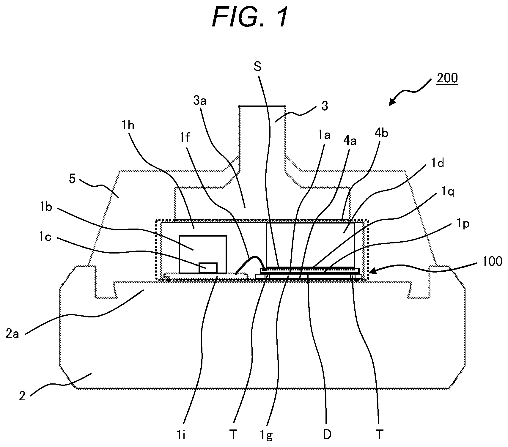
is a schematic vertical sectional view showing a semiconductor device according to a first embodiment.
is an enlarged vertical sectional view showing a semiconductor chip of and components located above and below the semiconductor chip.
is a plan view partially showing an electronic circuit body of .
is a partial vertical sectional view showing a semiconductor device having a structure of the related art.
is a partial vertical sectional view showing the semiconductor device according to the first embodiment.
is a vertical sectional view geometrically showing the same portion as the semiconductor device shown in .
is a graph showing an example of a result of estimating a thermal stress generated in the semiconductor chip according to the first embodiment by a finite element analysis.
is a graph showing an example of a result of estimating thermal resistance of a semiconductor device shown in by the finite element analysis.
is a vertical sectional view partially showing the semiconductor device in which a position of a grove is changed.
is a plan view partially showing an electronic circuit body according to a comparative example.
is a graph showing a result of a thermal stress analysis obtained by comparing the embodiment shown in with the comparative example shown in .
is a plan view partially showing an electronic circuit body according to a second embodiment.
is a cross-sectional view taken along a line B-B′ in .
is a partial vertical sectional view showing the vicinity of an end portion of a semiconductor chip according to the second embodiment.
is a plan view partially showing an electronic circuit body according to a third embodiment.
is a graph showing an effect of a configuration of .
DESCRIPTION OF THE PREFERRED EMBODIMENTS
The present disclosure relates to a structure of a semiconductor device, and particularly, to a technique effectively applied to a mounting structure of a power semiconductor for power control. The technique is particularly effective for the semiconductor device having a double-sided mounting structure.
Hereinafter, embodiments of the semiconductor device according to the present disclosure will be described in detail with reference to the drawings. The content of the present disclosure is not limited to the embodiments.
First Embodiment
is a schematic vertical sectional view showing a semiconductor device according to a first embodiment.
A semiconductor device 200 shown in is used as a rectifier element of an on-vehicle AC generator (alternator).
In , the semiconductor device 200 includes an electronic circuit body 100 , a base 2 including a pedestal 2 a at an upper portion thereof, and a lead 3 including a lead header 3 a at a lower portion thereof. The electronic circuit body 100 has a rectifying function. A range covered by the electronic circuit body 100 is shown by a dotted line. The base 2 and the lead 3 are terminals through which the electronic circuit body 100 is electrically connected to an external circuit. Further, the pedestal 2 a and a part located on the upper portion of the base 2 , the lead header 3 a and a part located on the lower portion of the lead 3 , and the electronic circuit body 100 are covered and sealed with a mold resin 5 .
The electronic circuit body 100 includes a semiconductor chip 1 a (semiconductor chip), a capacitor 1 b , and a control circuit chip 1 c . In addition, the electronic circuit body 100 includes a lower electrode 1 g , an upper electrode 1 d (source block), and a lead frame 1 i.
The pedestal 2 a and the lower electrode 1 g of the electronic circuit body 100 are connected via a conductive bonding material 4 a . The lead header 3 a and the upper electrode 1 d of the electronic circuit body 100 are connected via a conductive bonding material 4 b . In the present specification, the lower electrode 1 g is also referred to as a “first electrode”, and the upper electrode 1 d is also referred to as a “second electrode”.
In the present embodiment, the semiconductor chip 1 a is a MOSFET. The MOSFET includes a drain electrode D and a source electrode S. In , the drain electrode D is provided on a lower surface portion, and the source electrode S is provided on an upper surface portion. That is, the semiconductor chip 1 a has the double-sided mounting structure. A surface of the semiconductor chip 1 a on a side where the drain electrode D is provided is referred to as a “first main surface” of the semiconductor chip 1 a , and a surface of the semiconductor chip 1 a on a side where the source electrode S is provided is referred to as a “second main surface” of the semiconductor chip 1 a.
The drain electrode D is connected to an upper surface portion of the lower electrode 1 g , which is a first internal electrode, via a conductive bonding material 1 p . However, when the conductive bonding material 1 p is not used, the drain electrode D may be connected by ultrasonic bonding or the like.
The source electrode S is connected to a lower surface portion of the upper electrode 1 d , which is a second internal electrode, via a conductive bonding material 1 q . However, when the conductive bonding material 1 q is not used, the source electrode S may be connected by ultrasonic bonding or the like.
The control circuit chip 1 c is connected to an upper surface portion of the lead frame 1 i , which is a support, via a conductive bonding material.
The capacitor 1 b that supplies power to the control circuit chip 1 c is also connected to the upper surface portion of the lead frame 1 i via the conductive bonding material. As the capacitor 1 b , for example, a ceramic capacitor can be used.
A lower surface portion of the lower electrode 1 g is exposed from a lower surface portion of the electronic circuit body 100 without being covered with the mold resin 5 . The lower surface portion of the lower electrode 1 g is connected to the pedestal 2 a via the conductive bonding material 4 a.
An upper surface portion of the upper electrode 1 d is exposed from an upper surface portion of the electronic circuit body 100 . The upper surface portion of the upper electrode 1 d is connected to the lead header 3 a via the conductive bonding material 4 b.
Materials of the conductive bonding materials 1 p , 1 q , 4 a , 4 b , and the like are commonly used solders, alloys containing Au, Ag, or Cu, conductive adhesive materials, and the like. As the solder, a general high-lead solder, a eutectic solder, a lead-free solder, and the like are used. As the conductive adhesive material, a material in which a metal filler such as Ag, Cu, or Ni is mixed with a resin, or a material composed only of metal is used. The materials of the conductive bonding materials 1 p , 1 q , 4 a , 4 b , and the like may be the same material or different materials. The conductive bonding materials 1 p and 1 q may be form of the same material or different materials above and below the semiconductor chip 1 a . The conductive bonding materials 4 a and 4 b may be formed of the same material or different materials above and below the electronic circuit body 100 .
As the materials of the base 2 , the lead 3 , and the lower electrode 1 g , the upper electrode 1 d , and the lead frame 1 i inside the electronic circuit body 100 , Cu having high thermal conductivity and excellent conductivity is mainly used, and CuMo, 42 alloy, Al, Au, Ag, or the like may be used. At this time, in order to improve connection stability, it is desirable to plate Au, Pd, Ag, Ni, or the like on a connection portion with the conductive bonding material.
The control circuit chip 1 c is electrically connected to the semiconductor chip 1 a via a wire 1 f . For example, when the semiconductor chip 1 a is a power MOSFET, the gate electrode formed on the semiconductor chip 1 a and the control circuit chip 1 c are connected via the wire 1 f , and the control circuit chip 1 c controls a gate voltage of the power MOSFET. Accordingly, a large current can flow through the semiconductor chip 1 a having a switching function.
Further, the capacitor 1 b is electrically connected to the semiconductor chip 1 a and the control circuit chip 1 c by the lead frame 1 i and the wire 1 f . The capacitor 1 b has a function of supplying power necessary for driving the control circuit chip 1 c.
The semiconductor chip 1 a has a function of switching the large current. For example, the semiconductor chip (switching circuit chip) 1 a having the switching function is a semiconductor chip including an IGBT, a gate turn-off thyristor (GTO), and a power MOSFET. The semiconductor chip 1 a is a thyristor or the like that performs on/off control of the large current, and may be made of Si, SiC, SiN, GaAs, or the like.
The control circuit chip 1 c is a semiconductor chip that controls the semiconductor chip 1 a that switches the large current. The control circuit chip 1 c itself is a semiconductor chip that does not include the semiconductor chip that switches the large current. That is, the control circuit chip 1 c is a semiconductor chip in which, for example, a plurality of logic circuits, analog circuits, driver circuits, and the like are provided, and a microprocessor and the like are formed as necessary. The control circuit chip 1 c may also have a function of controlling a large current flowing through the semiconductor chip 1 a.
The semiconductor chip 1 a , the control circuit chip 1 c , the capacitor 1 b , the lower electrode 1 g , the upper electrode 1 d , and the conductive bonding materials 1 p and 1 q are entirely covered and sealed with a resin 1 h . Thereby, the electronic circuit body 100 is formed.
The lower surface portion of the lower electrode 1 g and the upper surface portion of the upper electrode 1 d are exposed to an outside of the electronic circuit body 100 without being covered with the resin 1 h of the electronic circuit body 100 .
Therefore, the upper surface portion of the upper electrode 1 d of the electronic circuit body 100 can be electrically connected to the lead header 3 a via the conductive bonding material 4 b . The lower surface portion of the lower electrode 1 g of the electronic circuit body 100 can be electrically connected to the pedestal 2 a via the conductive bonding material 4 a.
As described above, the electronic circuit body 100 is sealed with the resin 1 h and is integrally formed. An exposed portion of the lower electrode 1 g is electrically connected to the pedestal 2 a of the base 2 via the conductive bonding material 4 a . An exposed portion of the upper electrode 1 d is electrically connected to the lead header 3 a of the lead 3 via the conductive bonding material 4 b . The semiconductor device 200 is formed by covering the entire electronic circuit body 100 and a part of the base 2 and the lead 3 with the mold resin 5 .
The electronic circuit body 100 is reversed upside down at the time of manufacturing so that P and N polarities of the semiconductor device 200 can be switched.
As shown in , it is desirable that the upper electrode 1 d connected to the source electrode S of the semiconductor chip 1 a is thicker than the lower electrode 1 g . Here, increasing a thickness means increasing a length in a direction from the pedestal 2 a to the lead header 3 a.
Since a heat capacity of the upper electrode 1 d becomes larger by increasing a thickness of the upper electrode 1 d , heat generated due to a loss when a current flows through the source electrode S can be absorbed on an upper electrode 1 d side. Accordingly, an increase in temperature of the semiconductor chip 1 a can be prevented.
By increasing the thickness of the upper electrode 1 d , the upper electrode 1 d can be higher than the capacitor 1 b , and the upper electrode 1 d can be connected to the lead header 3 a as a terminal of the electronic circuit body 100 .
is an enlarged vertical sectional view showing the semiconductor chip 1 a of and components located above and below the semiconductor chip 1 a.
As shown in , the semiconductor chip 1 a (semiconductor chip) includes the drain electrode D (first main electrode) on a surface (one surface) on a lower electrode 1 g side, and a gate electrode C (not shown, see ) and the source electrode S (second main electrode) on a surface (the other surface) on the upper electrode 1 d side. The semiconductor chip 1 a includes a surface protective film L (guard ring) on an outer peripheral portion of a surface on a gate electrode C side.
The lower electrode 1 g is a plate-shaped electrode.
A surface of the semiconductor chip 1 a on a source electrode S side is connected to the lower surface portion of the upper electrode 1 d via the conductive bonding material 1 q . A surface on a drain electrode D side is connected to the upper surface portion of the lower electrode 1 g via the conductive bonding material 1 p . The conductive bonding materials 1 p and 1 q are also simply referred to as “bonding materials”. The conductive bonding material 1 p may be referred to as a “first bonding material” and the conductive bonding material 1 q may be referred to as a “second bonding material” so as to be distinguished from each other.
A length of the upper electrode 1 d is shorter than that of the semiconductor chip 1 a . Both an end portion of the upper electrode 1 d and an end portion of a connection portion between the upper electrode 1 d and the semiconductor chip 1 a are inside the semiconductor chip 1 a . An end portion of the lower electrode 1 g connected to the semiconductor chip 1 a is located outside an end portion of the semiconductor chip 1 a . The lower electrode 1 g is provided with grooves T. The grooves T each penetrate in a thickness direction of the lower electrode 1 g . At least a part of the groove T of the lower electrode 1 g overlaps the semiconductor chip 1 a . The groove T can be formed by press working or etching.
In summary, the lower electrode 1 g is the plate-shaped electrode and has the groove T in a region overlapping with the semiconductor chip 1 a.
is a plan view partially showing the electronic circuit body 100 of . A cross-section taken along a line A-A′ in corresponds to the cross-section in .
As shown in , the semiconductor chip 1 a (semiconductor chip) includes the gate electrode C on the surface (the other surface) on the upper electrode 1 d side.
Four grooves T are provided along a longitudinal direction of the lower electrode 1 g , and each have a shape that reaches the end portion of the lower electrode 1 g . In other words, the grooves T penetrate in the thickness direction of the first electrode, and each have the shape that reaches the end portion of the first electrode when viewed in a plan view.
The grooves T provided in the lower electrode 1 g reach an outer peripheral line G of the lower electrode 1 g (emphasized by a broken line in ). When the grooves T reach the end portion of the lower electrode 1 g , deformation of the semiconductor chip 1 a due to a thermal stress can be suppressed as described later.
Next, a method of manufacturing the electronic circuit body 100 , which is a component of the semiconductor device 200 , will be described.
First, the lower electrode 1 g , one conductive bonding material, the semiconductor chip 1 a , the other conductive bonding material, and the upper electrode 1 d are stacked in this order. The stacked layers are heated to melt the conductive bonding materials to form layers of the conductive bonding materials 1 p and 1 q . Then, the stacked layers are cooled to room temperature.
In a cooling step, thermal strain is generated in all of the upper electrode 1 d , the lower electrode 1 g , and the semiconductor chip 1 a . Since when the upper electrode 1 d and the lower electrode 1 g are Cu and the semiconductor chip 1 a is Si, respective thermal expansion coefficients are 16.8×10 −6 [K −1 ] and 2.4×10 −6 [K −1 ], the upper electrode 1 d and the lower electrode 1 g shrink more than the semiconductor chip 1 a . Accordingly, bending deformation occurs in the upper electrode 1 d , the lower electrode 1 g , and the semiconductor chip 1 a , and the thermal stress is generated in each member.
is a partial vertical sectional view showing a semiconductor device having a structure of the related art.
In , a portion corresponding to a region Y in is enlarged and shown.
As shown in , in the structure of the related art, a length of the lower electrode 1 g is longer than that of the semiconductor chip 1 a . The length of the upper electrode 1 d is shorter than that of the semiconductor chip 1 a . Therefore, the length of the conductive bonding material 1 p provided between the lower electrode 1 g and the semiconductor chip 1 a is longer than that of the conductive bonding material 1 q provided between the upper electrode 1 d and the semiconductor chip 1 a.
Since the lower electrode 1 g and the upper electrode 1 d shrink more than the semiconductor chip 1 a during cooling, a force applied to the semiconductor chip 1 a from the conductive bonding material 1 p is larger than a force applied to the semiconductor chip 1 a from the conductive bonding material 1 q . Therefore, the semiconductor chip 1 a after cooling has an upward-convex shape.
At a point p 1 shown in , due to the bending deformation of the semiconductor chip 1 a , tensile stress of an arrow Tb is generated, and tensile stress of an arrow Tj is also generated from the conductive bonding material 1 p at the same time, so that the stress is concentrated at the point p 1 . When a highly rigid bonding material such as the lead-free solder or a sintered material is used for the conductive bonding materials 1 p and 1 q , the stress at the point p 1 increases, and a risk of cracking in the semiconductor chip 1 a increases.
is a partial vertical sectional view showing the semiconductor device according to the present embodiment.
In , the portion corresponding to the region Y in is enlarged and shown.
In , the groove T is provided in the lower electrode 1 g . The groove T penetrates in the thickness direction of the lower electrode 1 g . By the groove T, the stress in regions D 1 and D 2 of the semiconductor chip 1 a is generated separately. Therefore, the stress is smaller than that of the structure of the related art. Accordingly, the stress at the point p 1 can be greatly reduced.
When the groove T does not penetrate, influence of a continuous portion of the lower electrode 1 g remains, so that an effect of reducing the stress generated in the regions D 1 and D 2 cannot be sufficiently obtained.
It is desirable that a width U of the groove T is wider than a thickness of the conductive bonding material 1 p . When the width U of the groove T is narrow, the conductive bonding material 1 p gets wet and spreads during manufacture, so that the groove T is filled with the conductive bonding material 1 p , and since the lower electrode 1 g is bonded between the regions D 1 and D 2 , the stress is transmitted through a bonding portion thereof. Such a configuration is not desirable because a stress reducing effect is lost.
By providing the groove T in the lower electrode 1 g , a highly reliable semiconductor device can be manufactured even when a highly rigid lead-free bonding material such as the lead-free solder or the sintered material is used as the conductive bonding material 1 p.
Further, by working out a position of the groove T, for example, aligning the groove T with the end portion of the upper electrode 1 d in a vertical direction, a heat dissipation path of the semiconductor chip 1 a can be secured, and an increase in thermal resistance can be suppressed. In other words, it is desirable that the groove T is provided at a position overlapping with the upper electrode 1 d . In this case, it is desirable that the groove T and the semiconductor chip 1 a overlap each other, and the upper electrode 1 d overlaps above the groove T.
Next, an effect of reducing the thermal stress and a change in the thermal resistance will be quantitatively described with reference to to 8 .
is a vertical sectional view geometrically showing the same portion as the semiconductor device shown in .
shows the definitions of coordinates and parameters used when examining the thermal stress and the thermal resistance generated in the manufactured semiconductor chip 1 a.
In , a direction parallel to an upper surface of the semiconductor chip 1 a and orthogonal to a longitudinal direction of the groove T is set as an x-axis. A distance from an end portion E-E′ (a right end of the upper electrode 1 d in ) of a connection surface of the upper electrode 1 d with the semiconductor chip 1 a to the end portion of the semiconductor chip 1 a is set to W. A distance from the end portion E-E′ to a center line F-F′ of the groove T (an axis of symmetry of the width of the groove T in a lateral direction) is set to J. In order to examine the case where the position of the groove T is changed, J is used as a parameter. When the center line F-F′ of the groove T is closer to a center of the semiconductor chip 1 a (on a left side in ) than the end portion E-E′ of the upper electrode 1 d , J takes a negative value. Herein, a parameter normalized by dividing J by W is defined as X.
In the example shown in , X=−0.4.
is a graph showing an example of a result of estimating the thermal stress generated in the semiconductor chip 1 a by a finite element analysis. A horizontal axis is X, and a vertical axis is a normalized thermal stress G.
The material of the upper electrode 1 d and the lower electrode 1 g is Cu, and the material of the semiconductor chip 1 a is Si. The material of the conductive bonding material 1 p is a solder containing Sn as a main component, which is a general lead-free bonding material. X is changed in a range of −2 to 2. σ on the vertical axis is a value normalized by using, as a numerator, a thermal stress generated at the point p 1 (a stress concentration position) of the semiconductor chip 1 a in , and using, as a denominator, a stress generated at the point p 1 when soft lead solder is used for the conductive bonding material 1 p in the structure of the related art shown in . Therefore, in the figure, σ=1 is indicated by a symbol Pb. In the solder containing Sn as the main component, a content of Sn is larger than a content of any other metal element in the metal elements contained in the solder.
As shown in , the stress becomes minimum when X is −0.4 and increases as X moves away from −0.4. When X is 0.3 and −1.2, the stress rises to the same level as the stress of the structure of the related art.
In summary, a distance from an end portion of a connection surface of the second electrode with the semiconductor chip to an end portion of the semiconductor chip is set to W, a distance from the end portion of the connection surface of the second electrode with the semiconductor chip to a center line of the groove T is set to J, and when J/W is defined as X, a position of the center line of the groove T satisfies the following Equation (1). −1.2< X< 0.3 (1)
is a graph showing an example of a result of estimating the thermal resistance by the finite element analysis. The horizontal axis is X, and the vertical axis is a normalized thermal resistance θ. X is changed in a range of −2 to 1. θ on the vertical axis is values obtained by normalizing the thermal resistances of the semiconductor device 200 shown in using, as the denominator, the thermal resistance of the semiconductor device 200 including the electronic circuit body 100 of the structure of the related art shown in . Therefore, in , θ=1 is indicated by a symbol CS. Here, the thermal resistance is defined by an increment from an initial state of the heat amount calculated from the temperature distribution of the semiconductor device 200 in a steady state in which the semiconductor chip 1 a operates and generates a predetermined heat generation amount. This is because it is considered that the larger this increment is, the smaller the heat dissipation to the outside is.
It can be seen from that the larger X is, that is, the closer the position of the groove T is to the end portion of the lower electrode 1 g , the larger the thermal resistance is. Therefore, in the range of X shown in , it is desirable that the position of the groove T is located inside the lower electrode 1 g because the thermal resistance is suppressed to be low.
Considering the thermal stress shown in and the thermal resistance shown in , it can be seen that when X is −0.4, the thermal stress is the minimum and the thermal resistance is also suppressed to be low.
By providing the groove T at the position where X=−0.4 as shown in , it is possible to suppress the concentration of the stress at the point p 1 and minimize the amount of deformation. Further, since the upper electrode 1 d is disposed directly above the groove T, it is possible to secure the heat dissipation path upward from the semiconductor chip 1 a and suppress the thermal resistance from the semiconductor chip 1 a.
In the present embodiment, the solder containing Sn as the main component is used as the conductive bonding material 1 p . Since the solder containing Sn as the main component has a high modulus of elasticity and a high thermal conductivity as compared with a solder containing Pb as the main component, it is considered that when the solder containing Sn as the main component is applied to the structure of the related art as shown in , the stress generated in the semiconductor chip 1 a increases and the thermal resistance decreases. Here, the stress needs to be considered, and by providing the groove T as in the present embodiment, the stress generated in the semiconductor chip 1 a can be suppressed to the same level as or less than that of the structure of the related art using the solder containing Pb as the main component. In the present embodiment, the thermal resistance is increased by providing the groove T, and since the solder containing Sn as the main component is used, the thermal resistance can also be suppressed. Even when another Pb-free bonding material such as a sintered metal using Cu or Ag is used, it is expected that the same tendency is qualitatively obtained when the elastic modulus of the Pb-free bonding material is higher than that of Pb and the thermal conductivity thereof is higher than that of Pb.
The effect of the present embodiment is not limited to X=−0.4.
is a vertical sectional view partially showing the semiconductor device in which the position of the groove T is changed.
In , the groove T is disposed such that the center line F-F′ of the groove T is located outside the end portions E-E′. That is, in the example, X=0.25. Also, in this example, it can be said that the groove T is provided at a position overlapping with the second electrode.
In , since a region where the upper electrode 1 d overlaps is small just above the groove T, the heat dissipation path upward from the semiconductor chip 1 a is smaller than that when X=−0.4 shown in , but the increase amount of the thermal resistance is small as shown in .
It can be seen from that even if X=0.25 as in the example of , the stress can be the same as that of the structure of the related art. Therefore, the stress reducing effect can be obtained even when X=−0.4 cannot be realized due to the restrictions of the electronic circuit body 100 .
Next, the necessity that the groove T reaches the end portion of the lower electrode 1 g will be described.
is a plan view partially showing an electronic circuit body according to a comparative example.
In , the grooves T do not reach the outer peripheral line G of the lower electrode 1 g . The configuration other than the grooves T is the same as that in . The lower electrode 1 g is connected by an outer peripheral region H (a rectangle shown by a broken line in contact with the end portion of the lower electrode 1 g in ). Therefore, the stress generated on both sides of the outer peripheral region H is transmitted without being divided, and an effect of reducing the stress applied to the semiconductor chip 1 a cannot be obtained. Therefore, thermal deformation of the semiconductor chip 1 a tends to be large.
is a graph showing a result of a thermal stress analysis obtained by comparing the embodiment shown in with the comparative example shown in . In both the embodiment and the comparative example, the solder containing Sn as the main component, which is the lead-free bonding material, is used. The vertical axis represents the normalized stress σ as in . A stress when the lead solder is used for the conductive bonding material 1 p is used as the denominator when the stress is normalized.
As shown in , the stress σ is as high as 1.48 in a comparative example Cm compared with 1.22 in an embodiment Ex. From this result, it can be seen that it is desirable that the groove T reaches the end portion of the lower electrode 1 g.
Second Embodiment
Next, a semiconductor device according to a second embodiment will be described with reference to to 14 .
is a plan view partially showing an electronic circuit body according to the present embodiment.
In , a width of the lower electrode 1 g is small, and an end portion Te thereof is located inside the semiconductor chip 1 a . The lower electrode 1 g is provided with the grooves T.
is a cross-sectional view taken along a line B-B′ in .
In , the end portion of the lower electrode 1 g is located inside the semiconductor chip 1 a.
is a partial vertical sectional view showing the vicinity of an end portion of the semiconductor chip according to the present embodiment.
As shown in , the lower electrode 1 g is not bonded in the region D 2 located at the end portion of the semiconductor chip 1 a . Therefore, for example, when the lower electrode 1 g is thermally shrunk in a cooling process of a reflow step or a flow step, the end portion of the semiconductor chip 1 a is not subjected to the stress from the lower electrode 1 g . Accordingly, the stress at the point p 1 can be reduced.
A configuration in which the end portion of the lower electrode 1 g is located inside the end portion of the semiconductor chip 1 a can also be applied to the configuration in which the grooves T are provided. The stress at the point p 1 can be further reduced as compared with a configuration in which the grooves T are only provided in the lower electrode 1 g.
Third Embodiment
is a plan view partially showing an electronic circuit body according to a third embodiment.
In , grooves T that reach the end portion along the longitudinal direction of the lower electrode 1 g are provided, and grooves T 2 are provided in two of the four grooves T. The grooves T 2 are provided along the lateral direction of the lower electrode 1 g . The grooves T 2 are provided so as to communicate with the grooves T in the middle of the grooves T. In other words, the grooves T include branched grooves T 2 .
The configuration of the present embodiment is a configuration of the first embodiment shown in with the grooves T 2 added.
With such a configuration, the thermal deformation of the semiconductor chip 1 a in both the longitudinal direction and the lateral direction of the lower electrode 1 g can be suppressed, and the stress generated in the semiconductor chip 1 a can be further reduced.
is a graph showing an effect of a configuration of . Conditions are similar to those in .
As shown in , the thermal stress σ of the present embodiment (Ex3) is 1.17, which is smaller than that of the first embodiment (Ex1). Therefore, if the grooves T 2 are added to the grooves T, an effect of further reducing the thermal stress can be obtained.
Hereinafter, the effects obtained by the semiconductor device of the present disclosure will be collectively described.
According to the semiconductor device of the present disclosure, it is possible to reduce the stress generated in the semiconductor chip, suppress the increase in the thermal resistance, and improve reliability.
Since the stress can be reduced, damage to the semiconductor chip can be prevented.
Since the increase in the thermal resistance can be suppressed, the failure of the semiconductor chip can be prevented.
Not only in a semiconductor device having a single-sided mounting structure but also in a semiconductor device having the double-sided mounting structure, it is possible to suppress the increase in temperature and prevent failure even if the current during use is increased.
Figures (9)
Citations
This patent cites (19)
- US2007/0145540
- US2021/0143081
- US2021/0287971
- US3171401
- US3823019
- US5332672
- US554983
- USS56-104458
- US5766655
- US6366958
- USH0422162
- USH04-333275
- US0823068
- USH10-163407
- US2007-173680
- US2008-034416
- US2014-107506
- US2021-77777
- US2021-077777