Reducing Precharge Power Consumption in a Memory Array
Abstract
An output node of a cell of a memory device is precharged based on an activation input for the cell. A memory device includes precharge circuitry configured to precharge an output node of a cell of the memory device based on an activation input for the cell.
Claims (20)
1. A method of operating a memory device, the method comprising: precharging an output node of a cell of the memory device based on an activation input for the cell, wherein the activation input controls whether to enable precharging of the output node.
11. A memory device comprising: precharge circuitry configured to precharge an output node of a cell of the memory device based on an activation input for the cell, wherein the activation input controls whether to enable the precharge circuitry to precharge the output node.
Show 18 dependent claims
2. The method of claim 1 , wherein the precharging is performed when the activation input has a first logic level.
3. The method of claim 1 , wherein the precharging is performed through coupling the output node to a power rail using a transistor.
4. The method of claim 3 , wherein the transistor comprises a PMOS transistor.
5. The method of claim 1 , wherein the memory device is a compute-in-memory device and the cell comprises a memory cell and calculation circuitry configured to perform a calculation based on the activation input and a value stored in the memory cell.
6. The method of claim 5 , wherein the calculation comprises multiplication.
7. The method of claim 1 , further comprising precharging the output node in response to an enable signal.
8. The method of claim 7 , further comprising producing a pulse in response to a change in the enable signal.
9. The method of claim 1 , wherein the cell stores a plurality of filter weights that are selectable based on a selection signal, and the method further comprises precharging the output node in response to a change in the selection signal.
10. The method of claim 1 , wherein the cell includes a static random access memory (SRAM) cell and/or a ternary content addressable memory (TCAM) cell.
12. The memory device of claim 11 , wherein the precharge circuitry precharges the output node when the activation input has a first logic level.
13. The memory device of claim 11 , wherein the precharge circuitry comprises a transistor configured to couple the output node to a power rail.
14. The memory device of claim 13 , wherein the transistor comprises a PMOS transistor.
15. The memory device of claim 11 , wherein the memory device is a compute-in-memory device and the cell comprises a memory cell and calculation circuitry configured to perform a calculation based on the activation input and a value stored in the memory cell.
16. The memory device of claim 15 , wherein the calculation comprises multiplication.
17. The memory device of claim 11 , wherein the precharge circuitry is configured to precharge the output node in response to an enable signal.
18. The memory device of claim 11 , wherein the precharge circuitry comprises a pulse generator.
19. The memory device of claim 11 , wherein the cell stores a plurality of filter weights that are selectable based on a selection signal, and the precharge circuitry is configured to precharge the output node in response to a change in the selection signal.
20. The memory device of claim 11 , wherein the cell includes a static random access memory (SRAM) cell and/or a ternary content addressable memory (TCAM) cell.
Full Description
Show full text →
CROSS-REFERENCE TO RELATED APPLICATIONS
This application claims priority to and the benefit of U.S. Provisional Application Ser. No. 63/322,251, filed Mar. 22, 2022 and entitled “METHOD AND APPARATUS FOR LOW POWER MULTIPLY AND ACCUMULATE (MAC) OPERATION IN A MEMORY ARRAY,” which is hereby incorporated herein by reference in its entirety.
BACKGROUND
In conventional computing devices, a memory functional block is separate from a processor functional block. Data is fetched from the memory to perform operations in the processor functional block.
Compute-in-memory (CIM) devices are devices in which operations may be performed in the memory. Such architectures may have the benefit of improved speed or lower power consumption. One example of an application for CIM devices is an implementing neural networks. Neural networks make extensive use of multiply accumulate operations, in which inputs are multiplied by filter weights and the products are summed. CIM devices may include hardware for performing the multiply and accumulate operations as well as memory cells for storing the filter weights.
SUMMARY
Some aspects relate to a method of operating a memory device, the method comprising precharging an output node of a cell of the memory device based on an activation input for the cell.
Some aspects relate to a memory device comprising precharge circuitry configured to precharge an output node of a cell of the memory device based on an activation input for the cell.
The foregoing summary is provided by way of illustration and is not intended to be limiting.
BRIEF DESCRIPTION OF DRAWINGS
The accompanying drawings are not intended to be drawn to scale. In the drawings, each identical or nearly identical component that is illustrated in various figures is represented by a like numeral. For purposes of clarity, not every component may be labeled in every drawing.
illustrates a high-level block diagram of a compute-in-memory (CIM) device having an array of CIM cells arranged in rows and columns.
is a block diagram showing functional circuit blocks of a CIM cell and functional circuit blocks that provide signals to a CIM cell.
shows additional detail of one example of a CIM cell in which calculation circuitry is configured to perform multiplication of the input A and value W stored in a memory cell.
A- 4 C show an embodiment for performing precharge based on an activation input.
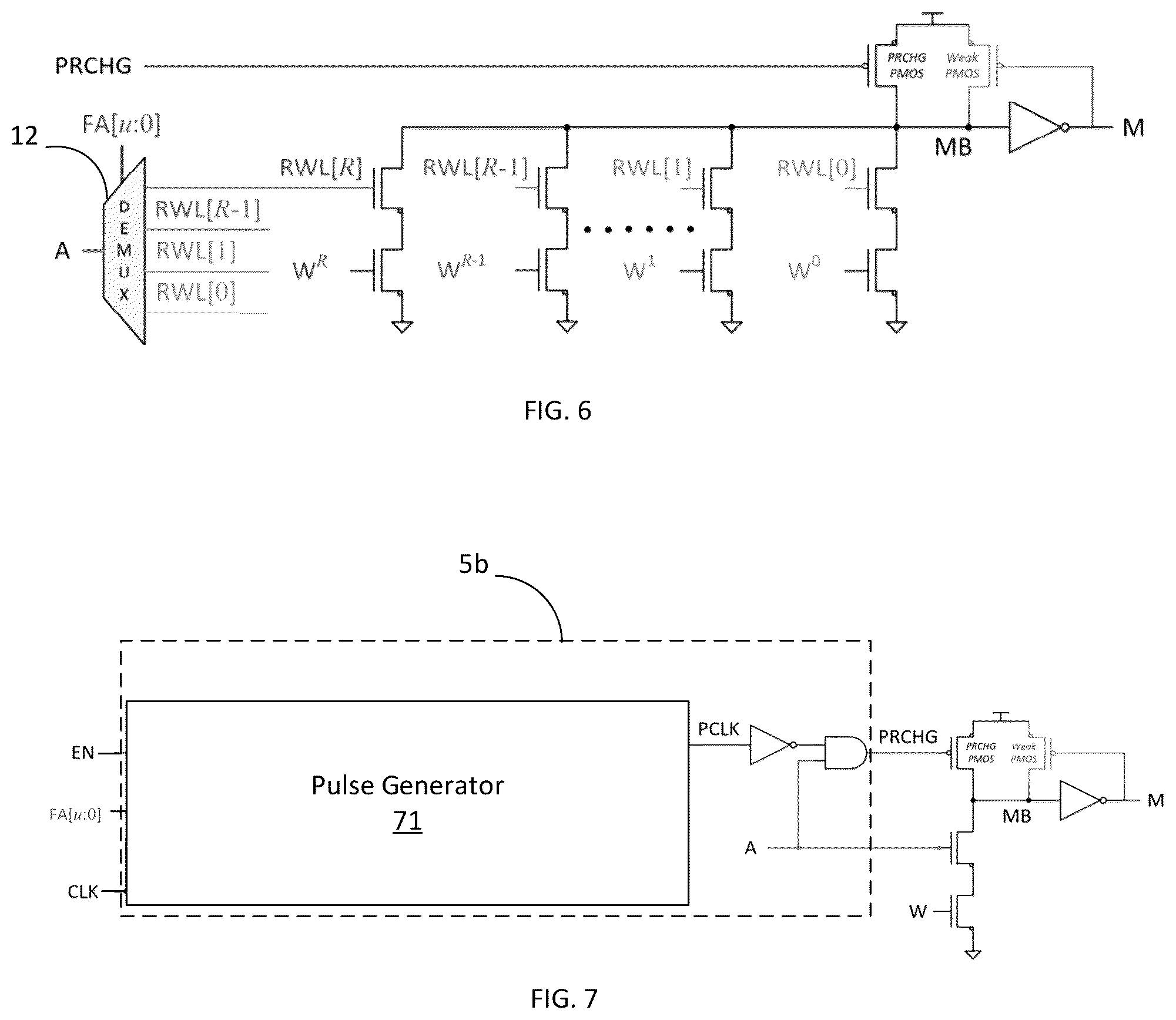
A- 5 B show an embodiment for performing precharge based on an activation input.
illustrates that a CIM cell 1 may have a plurality of memory cells storing respective weights W and a demultiplexer 12 that provides the input A to a transistor gate of a selected multiplier path corresponding to the selected weight W.
shows an example of precharge logic including a pulse generator configured to produce a pulse to initiate precharge in response to a change in any one or more of a plurality of input signals.
DETAILED DESCRIPTION
The devices and techniques described herein allow for reducing the power consumption in a memory array due to precharge operations. The inventors have recognized and appreciated that conventional techniques for precharging an output node of a cell cause frequent switching of a precharge device connected to the output node, which may lead to high power consumption due to frequent charging and discharging of the gate capacitance of the precharge device. The power consumption can be reduced by switching the precharge device less frequently. In some embodiments, a precharge operation for a memory cell may be triggered by an activation input corresponding to the memory cell. Since the activation signal changes values relatively infrequently, the precharge device may be switched less frequently, and the power consumption caused by precharge may be reduced. Such techniques may be used in a compute-in-memory (CIM) device or other devices having a memory array.
illustrates a high-level block diagram of a compute-in-memory (CIM) device 10 having an array of CIM cells 1 arranged in rows and columns. The CIM device 10 may have any number of rows and columns. Each CIM cell 1 has at least one memory cell and associated calculation circuitry, as discussed further below. The output node of the calculation circuitry needs to be precharged before performing a compute operation.
is a block diagram showing functional circuit blocks of a CIM cell 1 , according to some embodiments. The CIM cell 1 includes a memory cell 2 , calculation circuitry 3 that performs calculations based on an activation input A and the value W stored in the memory cell, and a precharge device 4 that precharges an output node of the calculation circuitry 3 . Precharge logic 5 may control the precharge device 4 to precharge the output node 7 of the calculation circuitry 3 with a suitable timing. In some embodiments, the precharge device 4 may be turned on (conductive) in response to the activation input A. After the precharge operation, the precharge device 4 is turned off (non-conductive). The calculation circuitry 3 is then ready to perform a calculation using the input A and the value W stored in the memory cell 2 when the CIM device 10 performs a compute operation. When the CIM device 10 controls calculation circuitry 3 to perform a compute operation, the result of the calculation is provided to output node 7 . The memory cell 2 may be any suitable type of memory cell, such as a static random access memory (SRAM) cell or a ternary content addressable memory (TCAM) cell, for example.
shows additional detail of one example of a CIM cell according to some embodiments. In this example, the calculation circuitry 3 a is configured to perform multiplication of the activation input A and value W stored in the memory cell 2 . The precharge logic 5 provides a signal PRCHG that controls precharge device 4 a to precharge the output node 7 a , also shown as node MB. The precharge device 4 a may be a PMOS transistor that is controlled to perform the precharge operation in response to signal PRCHG having a low logic level. During the precharge operation the precharge device 4 a is conductive, and connects output node 7 a to the power rail 8 . The CIM cell 1 may include an inverter 11 that inverts signal MB to produce signal M. Signal M may be provided to an adder tree to perform the addition portion of a multiply-accumulate calculation. When a compute operation is performed the input A is multiplied by the value W stored in the memory cell 2 . Values A and W may be digital values. If both A and W are logic high, the output node 7 a is pulled down to ground (logic low). If either A or W or both are logic low, the output node 7 a is not pulled down to ground and instead remains at the precharge voltage (logic high, in this example). The CIM cell 1 may include circuitry for maintaining MB at a high logic level when the precharge device is off and either A or W or both has a low logic level: in this example a weak PMOS device performs this function.
A shows a circuit diagram of an embodiment of a CIM cell in which the gate of the precharge device 4 a is connected to the activation input A. As shown in the truth table of B , when the activation input A has a logic value of zero the precharge device 4 a turns on and precharges node MB to the voltage of the power rail 8 . C shows a timing diagram illustrating an activation input A having a low logic value causing MB to be precharged to a high logic value. When a compute operation is performed and both A and W have high logic values, the node MB is pulled down to a low logic value.
A shows a diagram of another embodiment in which precharge logic 5 a produces a precharge signal PRCHG in response to the activation input A. The precharge logic 5 a includes a pulse generator 51 and other logic circuitry. With the precharge logic 5 , the precharge operation can be initiated either by logic signal A having a low logic level or in response to a pulse signal PCLK produce in response to an enable signal EN. B shows a timing diagram illustrating the signals shown in A , with signal PEN being an internal signal of the pulse generator 51 . In some embodiments, the enable signal EN may transition from a low logic level to a high logic level when a compute operation is enabled in the CIM device 10 . In response, the pulse generator 51 may produce a pulse that causes an initial precharge operation to be performed.
illustrates that a CIM cell may have a plurality of memory cells storing respective weights W and a demultiplexer 12 that provides the input A to a transistor gate of a selected multiplier path corresponding to the selected weight W. The selection signal FA[u:0] is the selection signal of the demultiplexer, which determines which filter weight W is selected, and applies the activation signal A to the gate of the transistor RWL corresponding to the selected weight W.
In some embodiments, the precharge operation may be triggered in response to a change in the selection signal FA[u:0]. To do so, the enable signal EN of the precharge logic 5 a may be the selection signal FA[u:0]. Alternatively or additionally, the precharge operation may be triggered in response to a change in any one of a plurality of signals, such as enable signal EN that switches to a logic high when a compute operation is enabled in the CIM device 10 , and FA[u:0]. The precharge logic 5 may activate the precharge operation in response to a change in any of such signals. shows an example of such precharge logic as precharge logic 5 b , which includes a pulse generator 71 configured to produce a pulse to initiate precharge in response to a change in either enable signal EN or selection signal FA[u:0].
Use of ordinal terms such as “first”, “second”, “third”, etc., in the claims to modify a claim element does not by itself connote any priority, precedence, or order of one claim element over another or the temporal order in which acts of a method are performed, but are used merely as labels to distinguish one claim element having a certain name from another element having a same name (but for use of the ordinal term) to distinguish the claim elements.
Also, the phraseology and terminology used herein is for the purpose of description and should not be regarded as limiting. The use of “including”, “comprising”, “having”, “containing” or “involving” and variations thereof herein, is meant to encompass the items listed thereafter and equivalents thereof as well as additional items.
The use of “coupled” or “connected” is meant to refer to circuit elements, or signals, that are either directly linked to one another or through intermediate components.
The terms “approximately”, “substantially,” and “about” may be used to mean within ±20% of a target value in some embodiments, within ±10% of a target value in some embodiments, within ±5% of a target value in some embodiments, and within ±2% of a target value in some embodiments. The terms “approximately” and “about” may include the target value.
Figures (1)
Citations
This patent cites (25)
- US6005813
- US7355873
- US9286980
- US9543015
- US9564184
- US10534839
- US10621489
- US11018687
- US11049013
- US2015/0131383
- US2016/0225437
- US2019/0102671
- US2019/0103156
- US2020/0258569
- US2020/0301668
- US2020/0403616
- US2021/0012202
- US2021/0027815
- US2021/0240442
- US2021/0350846
- US2022/0044714
- US2022/0301605
- US2022/0328099
- US2023/0022347
- US2019/246064