Display Panel and Display Device Including the Same
Abstract
A display panel includes 11-th to 15-th pixel circuits arranged in a first row, 21-th to 25-th pixel circuits arranged in a second row, 11-th to 14-th light-emitting elements, each being connected to corresponding one of the 11-th to 15-th pixel circuits, and 21-th to 24-th light-emitting elements, each being connected to corresponding one of the 21-th to 25-th pixel circuits. The 11-th light-emitting element is connected to one of the 11-th to 15-th pixel circuits overlapping therewith, wherein the 13-th light-emitting element is connected to one of the 11-th to 15-th pixel circuits non-overlapping therewith via a first connection wiring, wherein the 21-th light-emitting element is connected to one of the 21-th to 25-th pixel circuits overlapping therewith, wherein the 23-th light-emitting element is connected to one of the 21-th to 25-th pixel circuits non-overlapping therewith via a second connection wiring.
Claims (27)
1. A display panel comprising: a plurality of data lines which include first to fifth data lines; a plurality of pixel circuits which include 11-th to 15-th pixel circuits respectively connected to the first to fifth data lines and arranged in a first row, and 21-th to 25-th pixel circuits respectively connected to the first to fifth data lines and arranged in a second row; and a plurality of light-emitting elements which include 11-th to 14-th light-emitting elements, each being connected to corresponding one of the 11-th to 15-th pixel circuits, and 21-th to 24-th light-emitting elements, each being connected to corresponding one of the 21-th to 25-th pixel circuits, wherein the 11-th light-emitting element is connected to one of the 11-th to 15-th pixel circuits which overlaps the 11-th light-emitting element, wherein the 13-th light-emitting element is connected to one of the 11-th to 15-th pixel circuits which does not overlap the 13-th light-emitting element via a first connection wiring, wherein the 21-th light-emitting element is connected to one of the 21-th to 25-th pixel circuits which overlaps the 21-th light-emitting element, wherein the 23-th light-emitting element is connected to one of the 21-th to 25-th pixel circuits which does not overlap the 23-th light-emitting element via a second connection wiring, wherein the 11-th light-emitting element and the 23-th light-emitting element emit light of the same color, wherein the 13-th light-emitting element and the 21-th light-emitting element emit light of the same color, and wherein the 13-th light-emitting element and the 23-th light-emitting element emit light of different colors, respectively.
16. A display device comprising: a display panel; a data driver circuit electrically connected to a first output line, a second output line, and a third output line; and a demultiplexer configured to alternately electrically connect the first output line to a first data line and a second data line, alternately electrically connect the second output line to a third data line and a fourth data line, and electrically connect the third output line to a fifth data line, wherein the display panel includes: a plurality of pixel circuits which include 11-th to 15-th pixel circuits respectively connected to the first to fifth data lines and arranged in a first row, and 21-th to 25-th pixel circuits respectively connected to the first to fifth data lines and arranged in a second row; and a plurality of light-emitting elements which include 11-th to 14-th light-emitting elements, each being connected to corresponding one of the 11-th to 15-th pixel circuits and 21-th to 24-th light-emitting elements, each being connected to corresponding one of the 21-th to 25-th pixel circuits, wherein the 11-th light-emitting element is connected to one of the 11-th to 15-th pixel circuits which overlaps the 11-th light-emitting element, wherein the 13-th light-emitting element is connected to one of the 11-th to 15-th pixel circuits which does not overlap the 13-th light-emitting element via a first connection wiring, wherein the 21-th light-emitting element is connected to one of the 21-th to 25-th pixel circuits which overlaps the 21-th light-emitting element, wherein the 23-th light-emitting element is connected to one of the 21-th to 25-th pixel circuits which does not overlap the 23-th light-emitting element via a second connection wiring, wherein the 11-th light-emitting element and the 23-th light-emitting element emit light of the same color, wherein the 13-th light-emitting element and the 21-th light-emitting element emit light of the same color, and wherein the 13-th light-emitting element and the 23-th light-emitting element respectively emit light of different colors.
24. A display panel comprising: a plurality of output lines which include a first output line and a second output liner; a plurality of pixel circuits which include a first pixel circuit and a second pixel circuit electrically connected to the first output line, a third pixel circuit and a fourth pixel circuit electrically connected to the second output line, and first to fourth light-emitting elements respectively connected to the first to fourth pixel circuits, wherein a light-emitting element overlapping at least one of the third pixel circuit and the fourth pixel circuit among the first to fourth light-emitting elements is electrically insulated from the third pixel circuit and the fourth pixel circuit, wherein, during a first period, a first data signal of the first output line is provided to the first pixel circuit, and a second data signal of the second output line is provided to the third pixel circuit, wherein, during a second period, a third data signal of the first output line is provided to the second pixel circuit, and a fourth data signal of the second output line is provided to the fourth pixel circuit, and wherein the second data signal and the fourth data signal have the same color.
Show 24 dependent claims
2. The display panel of claim 1 , wherein the 11-th to 14-th light-emitting elements are sequentially arranged in a first direction, and wherein the 21-th to 24-th light-emitting elements are sequentially arranged in the first direction.
3. The display panel of claim 1 , further comprising a demultiplexer configured to operate in response to a switching signal to alternately connect a first output line to the first data line and the second data line, configured to alternately connect a second output line to the third data line and the fourth data line, and configured to connect a third output line to the fifth data line.
4. The display panel of claim 3 , wherein each of the 11-th light-emitting element and the 23-th light-emitting element emits first color light, wherein each of the 12-th light-emitting element, the 14-th light-emitting element, the 22-th light-emitting element, and the 24-th light-emitting element emits second color light, and wherein each of the 13-th light-emitting element and the 21-th light-emitting element emits third color light.
5. The display panel of claim 4 , wherein the first output line alternately transmits a data signal corresponding to the first color light and a data signal corresponding to the third color light, wherein the second output line transmits a data signal corresponding to the second color light, and wherein the third output line transmits a data signal corresponding to the first color light.
6. The display panel of claim 5 , wherein the first data line transmits the data signal corresponding to the first color light, wherein the second data line transmits the data signal corresponding to the third color light, wherein each of the third data line and the fourth data line transmits the data signal corresponding to the second color light, and wherein the fifth data line transmits the data signal corresponding to the first color light.
7. The display panel of claim 1 , wherein the first connection wiring intersects the second data line and the third data line to overlap the second data line and the third data line, and wherein the second connection wiring intersects the fourth data line and the fifth data line to overlap the fourth data line and the fifth data line.
8. The display panel of claim 1 , wherein the first connection wiring intersects the fourth data line and the fifth data line to overlap the fourth data line and the fifth data line, and wherein the second connection wiring intersects the second data line and the third data line to overlap the second data line and the third data line.
9. The display panel of claim 1 , wherein each of the plurality of light-emitting elements includes an anode and a cathode, wherein the first connection wiring extends from the anode of the 13-th light-emitting element, and wherein the second connection wiring extends from the anode of the 23-th light-emitting element.
10. The display panel of claim 1 , wherein each of the 11-th light-emitting element and the 23-th light-emitting element emits blue color light, wherein each of the 12-th light-emitting element, the 14-th light-emitting element, the 22-th light-emitting element, and the 24-th light-emitting element emits green color light, and wherein each of the 13-th light-emitting element and the 21-th light-emitting element emits red color light.
11. The display panel of claim 1 , wherein each of the 11-th light-emitting element and the 23-th light-emitting element emits red color light, wherein each of the 12-th light-emitting element, the 14-th light-emitting element, the 22-th light-emitting element, and the 24-th light-emitting element emits green color light, and wherein each of the 13-th light-emitting element and the 21-th light-emitting element emits blue color light.
12. The display panel of claim 1 , wherein the 12-th light-emitting element is connected to the 13-th pixel circuit via a third connection wiring, wherein the 14-th light-emitting element is connected to the 14-th pixel circuit, wherein the 22-th light-emitting element is connected to the 23-th pixel circuit via a fourth connection wiring, and wherein the 24-th light-emitting element is connected to the 24-th pixel circuit.
13. The display panel of claim 1 , further comprising a demultiplexer including a first switch and a second switch, the demultiplexer being configured to: operate in response to a first switching signal applied to the first switch to connect first, second, and third output lines to the first, third, and fifth data lines, respectively; and operate in response to a second switching signal applied to the second switch to connect the first and second output lines to the second and fourth data lines, respectively, wherein, during a first frame, the first switching signal transitions to an active level before the second switching signal transitions to an active level, and wherein, during a second frame subsequent to the first frame, the second switching signal transitions to an active level before the first switching signal transitions to an active level.
14. The display panel of claim 1 , wherein some of the 11-th to 15-th pixel circuits in the first row are connected to a first scan line and others of the 11-th to 15-th pixel circuits in the first row are connected to a second scan line, and wherein some of the 21-th to 25-th pixel circuits in the second row are connected to a third scan line and others of the 21-th to 25-th pixel circuits in the second row are connected to a fourth scan line.
15. The display panel of claim 14 , wherein an activation period of each of scan signals respectively transmitted to the first to fourth scan lines is longer than a half of one horizontal period.
17. The display device of claim 16 , wherein the demultiplexer is configured to operate in response to a switching signal to alternately electrically connect the first output line to the first data line and the second data line, and to alternately electrically connect the second output line to the third data line and the fourth data line, and to electrically connect the third output line to the fifth data line.
18. The display device of claim 16 , wherein the 11-th to 14-th light-emitting elements are sequentially arranged in a first direction, and wherein the 21-th to 24-th light-emitting elements are sequentially arranged in the first direction.
19. The display device of claim 16 , wherein each of the 11-th light-emitting element and the 23-th light-emitting element emits first color light, wherein each of the 12-th light-emitting element, the 14-th light-emitting element, the 22-th light-emitting element, and the 24-th light-emitting element emits second color light, and wherein each of the 13-th light-emitting element and the 21-th light-emitting element emits third color light.
20. The display device of claim 19 , wherein the data driver circuit is configured to: alternately output a data signal corresponding to the first color light and a data signal corresponding to the third color light to the first output line; output a data signal corresponding to the second color light to the second output line; and output a data signal corresponding to the first color light to the third output line.
21. The display device of claim 20 , wherein the first data line transmits the data signal corresponding to the first color light, wherein the second data line transmits the data signal corresponding to the third color light, wherein each of the third data line and the fourth data line transmits the data signal corresponding to the second color light, and wherein the fifth data line transmits the data signal corresponding to the first color light.
22. The display device of claim 16 , wherein the first connection wiring intersects the second data line and the third data line to overlap the second data line and the third data line, and wherein the second connection wiring intersects the fourth data line and the fifth data line to overlap the fourth data line and the fifth data line.
23. The display device of claim 16 , wherein the plurality of light-emitting elements includes an anode and a cathode, wherein the first connection wiring extends from the anode of the 13-th light-emitting element, and wherein the second connection wiring extends from the anode of the 23-th light-emitting element.
25. The display panel of claim 24 , wherein the first data signal, the second data signal, and the third data signal have different colors.
26. The display panel of claim 24 , wherein the first pixel circuit is electrically connected to the first light-emitting element, wherein the second pixel circuit is electrically connected to the third light-emitting element, wherein the third pixel circuit is electrically connected to the second light-emitting element, and wherein the fourth pixel circuit is electrically connected to the fourth light-emitting element.
27. The display panel of claim 26 , wherein the second light-emitting element and the fourth light-emitting element emit light of the same color.
Full Description
Show full text →
CROSS-REFERENCE TO RELATED APPLICATIONS
This application claims priority under 35 U.S.C. § 119 to Korean Patent Application No. 10-2022-0187911 filed on Dec. 28, 2022, in the Korean Intellectual Property Office, the disclosures of which are incorporated by reference herein in their entireties.
BACKGROUND
Embodiments of the present disclosure described herein relate to a display device.
In general, a display device includes a display panel for displaying an image and a driver circuit for driving the display panel. The display panel includes a plurality of scan lines, a plurality of data lines, and a plurality of pixels. The driver circuit includes a data driver circuit that outputs a data signal to the data lines, a scan driver circuit that outputs a scan signal to drive the scan lines, and a drive controller that controls the data driver circuit and the scan driver circuit.
This display device may display an image by outputting the scan signals to scan lines connected to pixels from which the image is to be displayed, and providing data voltages corresponding to the image to data lines connected to the pixels.
Further, each of the plurality of pixels may provide one of various color light such as red light, green light, and blue light. Each of the plurality of pixels may include a light-emitting element and a pixel circuit for driving the light-emitting element. A size of each of the plurality of pixels and an arrangement scheme thereof may vary.
SUMMARY
Embodiments of the present disclosure provide a display panel and display device with reduced power consumption.
A first aspect of the present disclosure provides a display panel including a plurality of data lines which include first to fifth data lines, a plurality of pixel circuits which include 11-th to 15-th pixel circuits respectively connected to the first to fifth data lines and arranged in a first row, and 21-th to 25-th pixel circuits respectively connected to the first to fifth data lines and arranged in a second row, a plurality of light-emitting element which include 11-th to 14-th light-emitting elements, each being connected to corresponding one of the 11-th to 15-th pixel circuits, and 21-th to 24-th light-emitting elements, each being connected to corresponding one of the 21-th to 25-th pixel circuits, wherein the 11-th light-emitting element is connected to one of the 11-th to 15-th pixel circuits which overlaps the 11-th light-emitting element, wherein the 13-th light-emitting element is connected to one of the 11-th to 15-th pixel circuits which does not overlap the 13-th light-emitting element via a first connection wiring, wherein the 21-th light-emitting element is connected to one of the 21-th to 25-th pixel circuits which overlaps the 21-th light-emitting element, wherein the 23-th light-emitting element is connected to one of the 21-th to 25-th pixel circuits which does not overlap the 23-th light-emitting element via a second connection wiring, wherein the 11-th light-emitting element and the 23-th light-emitting element emit light of the same color, wherein the 13-th light-emitting element and the 21-th light-emitting element emit light of the same color, wherein the 13-th light-emitting element and the 23-th light-emitting element emit light of different colors, respectively.
In one embodiment, the 11-th to 14-th light-emitting elements may be sequentially arranged in a first direction, wherein the 21-th to 24-th light-emitting elements may be sequentially arranged in the first direction.
In one embodiment, the display panel may further include a demultiplexer configured to operate in response to a switching signal to alternately connect a first output line to the first data line and the second data line, configured to alternately connect a second output line to the third data line and the fourth data line, and configured to connect a third output line to the fifth data line.
In one embodiment, each of the 11-th light-emitting element and the 23-th light-emitting element may emit first color light, wherein each of the 12-th light-emitting element, the 14-th light-emitting element, the 22-th light-emitting element, and the 24-th light-emitting element may emit second color light, wherein each of the 13-th light-emitting element and the 21-th light-emitting element may emit third color light.
In one embodiment, the first output line may alternately transmit a data signal corresponding to the first color light and a data signal corresponding to the third color light, wherein the second output line may transmit a data signal corresponding to the second color light, wherein the third output line may transmit a data signal corresponding to the first color light.
In one embodiment, the first data line may transmit the data signal corresponding to the first color light, wherein the second data line may transmit the data signal corresponding to the third color light, wherein each of the third data line and the fourth data line may transmit the data signal corresponding to the second color light, wherein the fifth data line may transmit the data signal corresponding to the first color light.
In one embodiment, the first connection wiring may intersect the second data line and the third data line to overlap the second data line and the third data line, and wherein the second connection wiring may intersect the fourth data line and the fifth data line to overlap the fourth data line and the fifth data line.
In one embodiment, the first connection wiring may intersect the fourth data line and the fifth data line to overlap the fourth data line and the fifth data line, wherein the second connection wiring may intersect the second data line and the third data line to overlap the second data line and the third data line.
In one embodiment, each of the plurality of light-emitting elements may include an anode and a cathode, wherein the first connection wiring may extend from the anode of the 13-th light-emitting element, wherein the second connection wiring may extend from the anode of the 23-th light-emitting element.
In one embodiment, each of the 11-th light-emitting element and the 23-th light-emitting element may emit blue color light, wherein each of the 12-th light-emitting element, the 14-th light-emitting element, the 22-th light-emitting element, and the 24-th light-emitting element may emit green color light, wherein each of the 13-th light-emitting element and the 21-th light-emitting element may emit red color light.
In one embodiment, each of the 11-th light-emitting element and the 23-th light-emitting element may emit red color light, wherein each of the 12-th light-emitting element, the 14-th light-emitting element, the 22-th light-emitting element, and the 24-th light-emitting element may emit green color light, wherein each of the 13-th light-emitting element and the 21-th light-emitting element may emit blue color light.
In one embodiment, the 12-th light-emitting element may be connected to the 13-th pixel circuit via a third connection wiring, wherein the 14-th light-emitting element may be connected to the 14-th pixel circuit, wherein the 22-th light-emitting element may be connected to the 23-th pixel circuit via a fourth connection wiring, wherein the 24-th light-emitting element may be connected to the 24-th pixel circuit.
In one embodiment, the display panel may further include a demultiplexer including a first switch and a second switch, the demultiplexer being configured to operate in response to the first switching signal applied to the first switch to connect first, second, and third output lines to the first, third, and fifth data lines, respectively, and operate in response to the second switching signal applied to the second switch to connect the first and second output lines to the second and fourth data lines, respectively, wherein, during a first frame, the first switching signal transitions to an active level before the second switching signal transitions to an active level, wherein, during a second frame subsequent to the first frame, the second switching signal transitions to an active level before the first switching signal transitions to an active level.
In one embodiment, some of the 11-th to 15-th pixel circuits in the first row may be connected to a first scan line and others of the 11-th to 15-th pixel circuits in the first row may be connected to a second scan line, wherein some of the 21-th to 25-th pixel circuits in the second row may be connected to a third scan line and others of the 21-th to 25-th pixel circuits in the second row may be connected to a fourth scan line.
In one embodiment, an activation period of each of scan signals respectively transmitted to the first to fourth scan lines may be longer than a half of one horizontal period.
A second aspect of the present disclosure provides a display device including a display panel, a data driver circuit electrically connected to a first output line, a second output line, and a third output line, and a demultiplexer configured to alternately electrically connect the first output line to a first data line and a second data line, alternately electrically connect the second output line to a third data line and a fourth data line, and electrically connect the third output line to a fifth data line, wherein the display panel includes a plurality of pixel circuits which include 11-th to 15-th pixel circuits respectively connected to the first to fifth data lines and arranged in a first row, and 21-th to 25-th pixel circuits respectively connected to the first to fifth data lines and arranged in a second row, and a plurality of light-emitting elements which include 11-th to 14-th light-emitting elements, each being connected to corresponding one of the 11-th to 15-th pixel circuits, and 21-th to 24-th light-emitting elements, each being connected to corresponding one of the 21-th to 25-th pixel circuits, wherein the 11-th light-emitting element is connected to one of the 11-th to 15-th pixel circuits which overlaps the 11-th light-emitting element, wherein the 13-th light-emitting element is connected to one of the 11-th to 15-th pixel circuits which does not overlap the 13-th light-emitting element via a first connection wiring, wherein the 21-th light-emitting element is connected to one of the 21-th to 25-th pixel circuits which overlaps the 21-th light-emitting element, wherein the 23-th light-emitting element is connected to one of the 21-th to 25-th pixel circuits which does not overlap the 23-th light-emitting element via a second connection wiring, wherein the 11-th light-emitting element and the 23-th light-emitting element emit light of the same color, wherein the 13-th light-emitting element and the 21-th light-emitting element emit light of the same color, wherein the 13-th light-emitting element and the 23-th light-emitting element respectively emit light of different colors.
In one embodiment, the demultiplexer may be configured to operate in response to a switching signal to alternately electrically connect the first output line to the first data line and the second data line, and to alternately electrically connect the second output line to the third data line and the fourth data line, and to electrically connect the third output line to the fifth data line.
In one embodiment, the 11-th to 14-th light-emitting elements may be sequentially arranged in a first direction, wherein the 21-th to 24-th light-emitting elements may be sequentially arranged in the first direction.
In one embodiment, each of the 11-th light-emitting element and the 23-th light-emitting element may emit first color light, wherein each of the 12-th light-emitting element, the 14-th light-emitting element, the 22-th light-emitting element, and the 24-th light-emitting element may emit second color light, wherein each of the 13-th light-emitting element and the 21-th light-emitting element may emit third color light.
In one embodiment, the data driver circuit may be configured to alternately output a data signal corresponding to the first color light and a data signal corresponding to the third color light to the first output line, output a data signal corresponding to the second color light to the second output line, and output a data signal corresponding to the first color light to the third output line.
In one embodiment, the first data line may transmit the data signal corresponding to the first color light, wherein the second data line may transmit the data signal corresponding to the third color light, wherein each of the third data line and the fourth data line may transmit the data signal corresponding to the second color light, wherein the fifth data line may transmit the data signal corresponding to the first color light.
In one embodiment, the first connection wiring may intersect the second data line and the third data line to overlap the second data line and the third data line, wherein the second connection wiring may intersect the fourth data line and the fifth data line to overlap the fourth data line and the fifth data line.
In one embodiment, the plurality of light-emitting elements may include an anode and a cathode, wherein the first connection wiring may extend from the anode of the 13-th light-emitting element, wherein the second connection wiring may extend from the anode of the 23-th light-emitting element.
A third aspect of the present disclosure provides a display panel including a plurality of pixel circuits which include first and second output lines, a first pixel circuit and a second pixel circuit electrically connected to the first output line, a third pixel circuit and a fourth pixel circuit electrically connected to the second output line and first to fourth light-emitting elements respectively connected to the first to fourth pixel circuits, wherein a light-emitting element overlapping at least one of the third pixel circuit and the fourth pixel circuit among the first to fourth light-emitting elements is electrically insulated from the third pixel circuit and the fourth pixel circuit, wherein, during a first period, a first data signal of the first output line is provided to the first pixel circuit, and a second data signal of the second output line is provided to the third pixel circuit, wherein, during a second period, a third data signal of the first output line is provided to the second pixel circuit, and a fourth data signal of the second output line is provided to the fourth pixel circuit, wherein the second data signal and the fourth data signal have the same color.
In one embodiment, the first data signal, the second data signal, and the third data signal may have different colors.
In one embodiment, the first pixel circuit may be electrically connected to the first light-emitting element, wherein the second pixel circuit may be electrically connected to the third light-emitting element, wherein the third pixel circuit may be electrically connected to the second light-emitting element, wherein the fourth pixel circuit may be electrically connected to the fourth light-emitting element.
In one embodiment, the second light-emitting element and the fourth light-emitting element may emit light of the same color.
BRIEF DESCRIPTION OF THE FIGURES
The above and other objects and features of the present disclosure will become apparent by describing in detail embodiments thereof with reference to the accompanying drawings.
is a block diagram of a display device according to an embodiment of the present disclosure.
is a diagram showing pixel circuits and light-emitting elements disposed in a display panel by way of example.
is a circuit diagram of a first-row pixel circuit and a second light-emitting element according to an embodiment of the present disclosure.
is a circuit diagram of a first-row pixel circuit, a second light-emitting element, a pixel circuit, and a first light-emitting element according to an embodiment of the present disclosure.
is a plan view of a display panel according to an embodiment of the present disclosure.
is a diagram illustrating a cross-section of a portion of each of a first light-emitting element and a first-row pixel circuit of a display panel according to an embodiment of the present disclosure by way of example.
is a diagram showing a cross-section of a portion of each of a third light-emitting element, a first-row pixel circuit, and another first-row pixel circuit of a display panel according to an embodiment of the present disclosure by way of example.
is a timing diagram for illustrating an operation of a display device.
is a plan view of a display panel according to an embodiment of the present disclosure.
is a plan view of a display panel according to an embodiment of the present disclosure.
is a plan view of a display panel according to an embodiment of the present disclosure.
is a timing diagram for illustrating an operation of a display device according to an embodiment of the present disclosure.
is a block diagram of a display device according to an embodiment of the present disclosure.
is a diagram showing pixel circuits and light-emitting elements disposed in a display panel according to an embodiment of the present disclosure.
is a timing diagram for illustrating an operation of a display device according to an embodiment of the present disclosure.
DETAILED DESCRIPTION
As used herein, when a component or a region, a layer, a portion, etc. is referred to as being “on”, “connected to”, or “coupled to” another component, it means that the component may be directly disposed/connected/coupled on another component or a third component may be disposed between the component and another component.
Like reference numerals refer to like components. In addition, in the drawings, thicknesses, ratios, and dimensions of components are exaggerated for effective description of technical content. “and/or” includes all of one or more combinations that the associated components may define.
Terms such as first, second, etc. may be used to describe various components, but the components should not be limited by the terms. The above terms are used only for the purpose of distinguishing one component from another. For example, without departing from the scope of the present disclosure, a first component may be named as a second component, and similarly, the second component may also be named as the first component. The singular expression includes the plural expression unless the context clearly dictates otherwise.
In addition, terms such as “beneath”, “below”, “on”, “above” are used to describe the relationship of the components illustrated in the drawings. The above terms are relative concepts, and are described with reference to directions indicated in the drawings.
It should be understood that terms such as “include” or “have” are intended to specify that a feature, a number, a step, an operation, a component, a part, or a combination thereof described in the specification is present, and do not preclude a possibility of addition or existence of one or more other features or numbers, steps, operations, components, parts, or combinations thereof.
Unless otherwise defined, all terms including technical and scientific terms used herein have the same meaning as commonly understood by one of ordinary skill in the art to which this disclosure belongs. It will be further understood that terms, such as those defined in commonly used dictionaries, should be interpreted as having a meaning that is consistent with their meaning in the context of the relevant art and will not be interpreted in an idealized or overly formal sense unless expressly so defined herein.
Hereinafter, embodiments of the present disclosure will be described with reference to drawings.
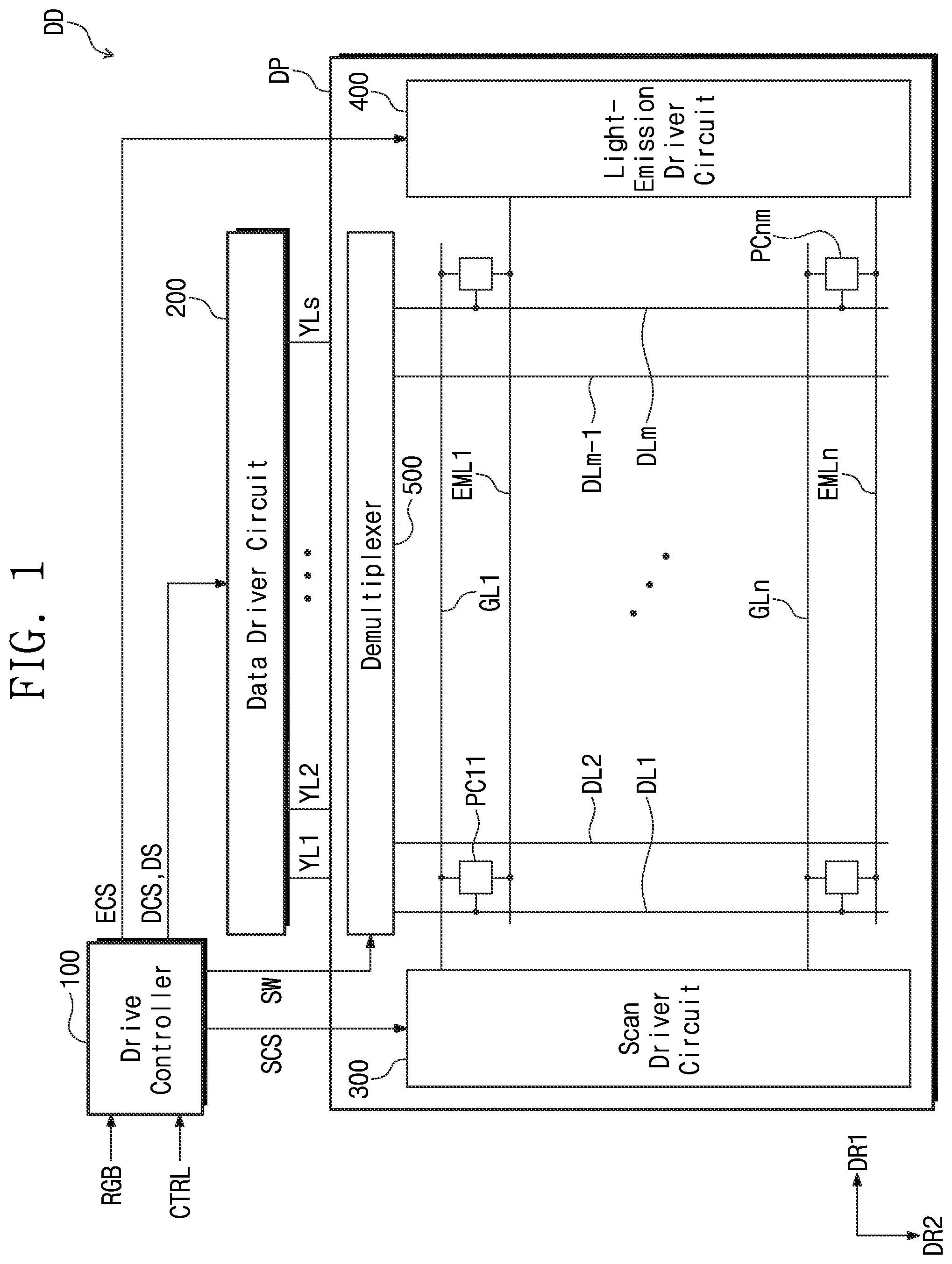
is a block diagram of a display device DD according to an embodiment of the present disclosure.
Referring to , the display device DD includes a drive controller 100 , a data driver circuit 200 , and a display panel DP.
The drive controller 100 receives an input image signal RGB and a control signal CTRL. The drive controller 100 generates an output image signal DS by converting the input image signal RGB into an image type suitable for the display panel DP. The drive controller 100 outputs a switching signal SW, a scan control signal SCS and a data control signal DCS.
The display panel DP according to an embodiment of the present disclosure may be a light-emitting display panel. For example, the display panel DP may be an organic light-emitting display panel, an inorganic light-emitting display panel, or a quantum dot light-emitting display panel. A light-emitting layer of the organic light-emitting display panel may include an organic light-emitting material. A light-emitting layer of the inorganic light-emitting display panel may include an inorganic light-emitting material. A light-emitting layer of the quantum dot light-emitting display panel may include a quantum dot, a quantum rod, or the like. Hereinafter, in this embodiment, an example in which the display panel DP is embodied as the organic light-emitting display panel is described.
The display panel DP includes scan lines GL 1 to GLn, data lines DL 1 to DLm, and pixel circuits PC 11 to PCnm. Although not shown in , the display panel DP may include a plurality of light-emitting elements. The plurality of light-emitting elements will be described in detail later.
The display panel DP may further include a scan driver circuit 300 , a light-emission driver circuit 400 and a demultiplexer 500 . Each of the pixel circuits PC 11 to PCnm may be electrically connected to the scan driver circuit 300 , the light-emission driver circuit 400 , and the demultiplexer 500 .
The scan lines GL 1 to GLn extend from the scan driver circuit 300 in a first direction DR 1 and are spaced apart from each other in a second direction DR 2 . The light-emission control lines EML 1 to EMLn extend from the light-emission driver circuit 400 in a direction opposite to the first direction DR 1 and are spaced apart from each other in the second direction DR 2 . The data lines DL 1 to DLm extend from the demultiplexer 500 in the second direction DR 2 and are spaced apart from each other in the first direction DR 1 .
Each of the pixel circuits PC 11 to PCnm may be connected to a corresponding scan line among the scan lines GL 1 to GLn (n is a positive integer), and may be connected to a corresponding data line among the data lines DL 1 to DLm (m is a positive integer), and may be connected to a corresponding light-emission control line among light-emission control lines EML 1 to EMLn. shows that each of the plurality of pixel circuits PC 11 to PCnm is connected to one scan line. However, the present disclosure is not limited thereto. Each of the plurality of pixel circuits PC 11 to PCnm may be electrically connected to two or more scan lines.
The data driver circuit 200 receives the data control signal DCS and the output image signal DS from the drive controller 100 . The data driver circuit 200 converts the output image signal DS into data signals, and outputs the data signals to output lines YL 1 to YLs (s is a positive integer). Each of the data signals may have a voltage level corresponding to a grayscale level of the output image signal DS. In an embodiment, the number of output lines YL 1 to YLs may be smaller than the number of data lines DL 1 to DLm (that is, s<m).
The data driver circuit 200 may be implemented as an integrated circuit (IC) and may be directly mounted on a predetermined area of the display panel DP. Alternatively, the data driver circuit 200 may be mounted on a separate printed circuit board in a chip on film (COF) scheme and then may be electrically connected to the display panel DP. In another embodiment, the data driver circuit 200 may be formed on the display panel DP in the same process as a process forming the pixel circuits PC 11 to PCnm.
The scan driver circuit 300 receives the scan control signal SCS from the drive controller 100 . The scan driver circuit 300 may output the scan signals to the scan lines GL 1 to GLn in response to the scan control signal SCS. In an embodiment, the scan driver circuit 300 may be formed in the same process as a process forming the pixel circuits PC 11 to PCnm.
The light-emission driver circuit 400 receives a light-emission drive signal ECS from the drive controller 100 . The light-emission driver circuit 400 may output the light-emission control signals to the light-emission control lines EML 1 to EMLn in response to the light-emission drive signal ECS. In an embodiment, the light-emission driver circuit 400 may be formed in the same process as a process forming the pixel circuits PC 11 to PCnm. shows the light-emission driver circuit 400 . However, the present disclosure is not limited thereto. In an embodiment, the light-emission driver circuit 400 may be embedded in the scan driver circuit 300 .
The drive controller 100 , the data driver circuit 200 , the scan driver circuit 300 , and the light-emission driver circuit 400 may be a driver circuit to provide the data signal corresponding to the input image signal RGB to the pixel circuits PC 11 to PCnm.
The demultiplexer 500 may electrically connect the plurality of output lines YL 1 to YLs to the data lines DL 1 to DLm in response to the switching signal SW provided from the drive controller 100 . A specific circuit configuration and operation of the demultiplexer 500 will be described in detail later.
shows that the demultiplexer 500 is disposed in the display panel DP. However, the present disclosure is not limited thereto. In an embodiment, the demultiplexer 500 may be included in the data driver circuit 200 . In an embodiment, the demultiplexer 500 may be provided in a separate driver circuit or circuit board independent from the display panel DP and the data driver circuit 200 .
is a diagram showing the pixel circuits and the light-emitting elements disposed in the display panel DP according to an embodiment of the present disclosure.
Referring to , the display panel DP includes the demultiplexer 500 , data lines DL 1 to DL 9 , the first-row pixel circuits PC 11 to PC 19 , the second-row pixel circuits PC 21 to PC 29 , first light-emitting elements BE 11 , BE 15 , BE 23 and BE 27 , second light-emitting elements GE 12 , GE 14 , GE 16 , GE 18 , GE 22 , GE 24 , GE 26 , and GE 28 , and third light-emitting elements RE 13 , RE 17 , RE 21 , and RE 25 . Sizes and arrangements of the first-row pixel circuits PC 11 to PC 19 , the second-row pixel circuits PC 21 to PC 29 , the first light-emitting elements BE 11 , BE 15 , BE 23 and BE 27 , the second light-emitting elements GE 12 , GE 14 , GE 16 , GE 18 , GE 22 , GE 24 , GE 26 , and GE 28 , and the third light-emitting elements RE 13 , RE 17 , RE 21 , and RE 25 as shown in are only examples to help understand the description. The present disclosure is not limited thereto.
In one embodiment, the first-row pixel circuits PC 11 to PC 19 may be referred to as 11-th to 19-th pixel circuits, respectively. The second-row pixel circuits PC 21 to PC 29 may be referred to as 21-th to 29-th pixel circuits, respectively.
Although not shown in the drawing, in one embodiment, each of the first-row pixel circuits PC 11 to PC 19 may be connected to a same scan line. In one embodiment, each of the second-row pixel circuits PC 21 to PC 29 may be connected to a same scan line.
The light-emitting elements may be referred to as the first light-emitting element, the second light-emitting element, and the third light-emitting element based on a color of light emitted therefrom. In one embodiment, the first light-emitting element BE 11 , the second light-emitting element GE 12 , the third light-emitting element RE 13 , the second light-emitting element GE 14 , the first light-emitting element BE 15 , the second light-emitting element GE 16 , the third light-emitting element RE 17 , and the second light-emitting element GE 18 may be referred to as 11-th to 18-th light-emitting elements BE 11 to GE 18 in an order in which they are arranged in the first direction DR 1 . Further, the third light-emitting element RE 21 , the second light-emitting element GE 22 , the first light-emitting element BE 23 , the second light-emitting element GE 24 , the third light-emitting element RE 25 , the second light-emitting element GE 26 , the first light-emitting element BE 27 , and the second light-emitting element GE 28 may be referred to as 21-th to 28-th light-emitting elements RE 21 to GE 28 in an order in which they are arranged in the first direction DR 1 .
The first light-emitting element BE 11 , the second light-emitting element GE 12 , the second light-emitting element GE 22 and the third light-emitting element RE 21 may be referred to as a first light-emitting area, a second light-emitting area, a third light-emitting area, and a fourth light-emitting area, respectively.
The demultiplexer 500 includes first switching transistors ST 1 , ST 3 , ST 5 , ST 7 and ST 9 and second switching transistors ST 2 , ST 4 , ST 6 and ST 8 .
The first switching transistor ST 1 is disposed between and connected to the output line YL 1 and the data line DL 1 . The first switching transistor ST 3 is disposed between and connected to the output line YL 2 and the data line DL 3 . The first switching transistor ST 5 is disposed between and connected to the output line YL 3 and the data line DL 5 . The first switching transistor ST 7 is disposed between and connected to the output line YL 4 and the data line DL 7 . The first switching transistor ST 9 is disposed between and connected to the output line YL 5 and the data line DL 9 . In an embodiment, the demultiplexer 500 may not include the first switching transistor ST 9 . In this case, the output line YL 5 may be directly connected to the data line DL 9 .
The second switching transistor ST 2 is disposed between and connected to the output line YL 1 and the data line DL 2 . The second switching transistor ST 4 is disposed between and connected to the output line YL 2 and the data line DL 4 . The second switching transistor ST 6 is disposed between and connected to the output line YL 3 and the data line DL 6 . The second switching transistor ST 8 is disposed between and connected to the output line YLA and the data line DL 8 .
The first switching transistors ST 1 , ST 3 , ST 5 , ST 7 and ST 9 are turned on in response to a first switching signal CLA, and the second switching transistors ST 2 , ST 4 , ST 6 and ST 8 are turned on in response to a second switching signal CLB. The switching signal SW provided from the drive controller 100 as shown in may include the first switching signal CLA and the second switching signal CLB. The first-row pixel circuits PC 11 to PC 19 may be sequentially arranged in a first row ROW 1 in the first direction DR 1 . The second-row pixel circuits PC 21 to PC 29 may be sequentially arranged in a second row ROW 2 in the first direction DR 1 .
The data lines DL 2 to DL 9 may be disposed adjacent to each other on two data lines basis. That is, the data lines DL 2 and DL 3 are disposed adjacent to each other between the first-row pixel circuits PC 12 and PC 13 . The data lines DLA and DL 5 are disposed adjacent to each other and between the first-row pixel circuits PC 14 and PC 15 . The data lines DL 6 and DL 7 are disposed adjacent to each other between the first-row pixel circuits PC 16 and PC 17 . The data lines DL 8 and DL 9 are disposed adjacent to each other between the first-row pixel circuits PC 18 and PC 19 . The first-row pixel circuits PC 11 to PC 19 and the second-row pixel circuits PC 21 to PC 29 are respectively connected to corresponding data lines among the data lines DL 1 to DL 9 . In an embodiment, some of the first-row pixel circuits PC 11 to PC 19 and the second-row pixel circuits PC 21 to PC 29 may be respectively connected to corresponding right data lines of the data lines DL 1 to DL 9 , while the others thereof may be respectively connected to corresponding left data lines of the data lines DL 1 to DL 9 .
In an embodiment, the first-row pixel circuits PC 12 , PC 14 , PC 16 and PC 18 , and the second-row pixel circuits PC 22 , PC 24 , PC 26 and PC 28 are connected to the data lines DL 2 , DL 4 , DL 6 and DL 8 adjacent thereto in a right direction, respectively. In an embodiment, the first-row pixel circuits PC 11 , PC 13 , PC 15 , PC 17 , and PC 19 , and the second-row pixel circuits PC 21 , PC 23 , PC 25 , PC 27 and PC 29 are connected to the data lines DL 1 , DL 3 , DL 5 , DL 7 and DL 9 adjacent thereto in a left direction, respectively.
The first light-emitting elements BE 11 and BE 15 , the second light-emitting elements GE 12 , GE 14 , GE 16 and GE 18 , and the third light-emitting elements RE 13 and RE 17 are arranged in the first row ROW 1 .
In the first row ROW 1 , the first light-emitting element BE 11 , the second light-emitting element GE 12 , the third light-emitting element RE 13 , the second light-emitting element GE 14 , the first light-emitting element BE 15 , the second light-emitting element GE 16 , the third light-emitting element RE 17 , and the second light-emitting element GE 18 may be sequentially arranged in the first direction DR 1 .
In the second row ROW 2 , the third light-emitting element RE 21 , the second light-emitting element GE 22 , the first light-emitting element BE 23 , the second light-emitting element GE 24 , the third light-emitting element RE 25 , the second light-emitting element GE 26 , the first light-emitting element BE 27 , and the second light-emitting element GE 28 be sequentially arranged in the first direction DR 1 .
In one embodiment, each of the first light-emitting elements BE 11 , BE 15 , BE 23 , and BE 27 may emit first color light, and each of the second light-emitting elements GE 12 , GE 14 , GE 16 , GE 18 , GE 22 , GE 24 , GE 26 , and GE 28 may emit second color light, and each of the third light-emitting elements RE 13 , RE 17 , RE 21 , and RE 25 may emit third color light.
In one embodiment, the first to third color light may be different color light.
In one embodiment, the first to third color light may be blue light, green light, and red light, respectively. However, the present disclosure is not limited thereto. In another embodiment, each of the first to third color light may be various color light such as blue light, green light, red light, white light, cyan light, magenta light, and yellow light.
The first light-emitting elements BE 11 and BE 15 of the first row ROW 1 are electrically connected to the first-row pixel circuits PC 11 and PC 15 , respectively. The second light-emitting elements GE 14 and GE 18 of the first row ROW 1 are electrically connected to the first-row pixel circuits PC 14 and PC 18 , respectively.
The second light-emitting elements GE 12 and GE 16 of the first row ROW 1 are electrically connected to the first-row pixel circuits PC 13 and PC 17 via connection wirings CL 12 and CL 16 , respectively. The third light-emitting elements RE 13 and RE 17 of the first row ROW 1 are electrically connected to the first-row pixel circuits PC 12 and PC 16 via connection wirings CL 13 and CL 17 , respectively.
The third light-emitting elements RE 21 and RE 25 of the second row ROW 2 are electrically connected to the second-row pixel circuits PC 22 and PC 26 , respectively. The second light-emitting elements GE 22 and GE 26 of the second row ROW 2 are electrically connected to the second-row pixel circuits PC 23 and PC 27 via connection wirings CL 22 and CL 26 , respectively.
The first light-emitting elements BE 23 and BE 27 of the second row ROW 2 are electrically connected to the second-row pixel circuits PC 25 and PC 29 via connection wirings CL 23 and CL 27 , respectively. The second light-emitting elements GE 24 and GE 28 of the second row ROW 2 are electrically connected to the second-row pixel circuits PC 24 and PC 28 , respectively.
The first-row pixel circuit PC 11 connected to the data line DL 1 is connected to the first light-emitting element BE 11 . In the example as shown in , no light-emitting element is connected to the second-row pixel circuit PC 21 connected to the data line DL 1 . In another embodiment, the display panel DP may not include the second-row pixel circuit PC 21 connected to the data line DL 1 .
The first-row pixel circuit PC 12 and the second-row pixel circuit PC 22 connected to the data line DL 2 are connected to the third light-emitting elements RE 13 and RE 21 , respectively.
The first-row pixel circuit PC 13 and the second-row pixel circuit PC 23 connected to the data line DL 3 are connected to the second light-emitting elements GE 12 and GE 22 , respectively.
The first-row pixel circuit PC 14 and the second-row pixel circuit PC 24 connected to the data line DLA are connected to the second light-emitting elements GE 14 and GE 24 , respectively.
The first-row pixel circuit PC 15 and the second-row pixel circuit PC 25 connected to the data line DL 5 are connected to the first light-emitting elements BE 15 and BE 23 , respectively.
The first-row pixel circuit PC 16 and the second-row pixel circuit PC 26 connected to the data line DL 6 are connected to the third light-emitting elements RE 17 and RE 25 , respectively.
The first-row pixel circuit PC 17 and the second-row pixel circuit PC 27 connected to the data line DL 7 are connected to the second light-emitting elements GE 16 and GE 26 , respectively.
The first-row pixel circuit PC 18 and the second-row pixel circuit PC 28 connected to the data line DL 8 are connected to the second light-emitting elements GE 18 and GE 28 , respectively.
The second-row pixel circuit PC 29 connected to the data line DL 9 is connected to the first light-emitting element BE 27 . In the example as shown in , no light-emitting element is connected to the first-row pixel circuit PC 19 connected to the data line DL 9 . In another embodiment, the display panel DP may not include the first-row pixel circuit PC 19 connected to the data line DL 9 .
As shown in , each of the data lines DL 1 to DL 9 is connected to the light-emitting element(s) emitting the same color light. Therefore, data signals of one color may be provided to each of the data lines DL 1 to DL 9 .
In particular, data signals G 3 and G 4 corresponding to the second color light are provided to the data lines DL 3 and DLA via the output line YL 2 and the first and second switching transistors ST 3 and ST 4 , respectively. Further, data signals G 7 and G 8 corresponding to the second color light are provided to the data lines DL 7 and DL 8 via the output line YL 4 and the first and second switching transistors ST 7 and ST 8 , respectively.
The data signals provided to the data lines DL 3 , DL 4 , DL 7 , and DL 8 from the data driver circuit 200 via the output lines YL 2 and YL 4 from the data driver circuit 200 may be the data signals G 3 , G 4 , G 7 , and G 8 corresponding to the same color such that power consumption of the data driver circuit 200 may be reduced.
is a circuit diagram of the first-row pixel circuit PC 11 and the first light-emitting element BE 11 according to an embodiment of the present disclosure.
shows the first-row pixel circuit PC 11 and the first light-emitting element BE 11 by way of example. In an embodiment, the first light-emitting element BE 11 may be a light-emitting diode. The first light-emitting element BE 11 may emit the first color light (e.g., blue light).
In an embodiment, the first-row pixel circuit PC 11 may include at least one transistor and at least one capacitor. The first-row pixel circuit PC 11 as shown in includes first to seventh transistors T 1 , T 2 , T 3 , T 4 , T 5 , T 6 , and T 7 and a capacitor Cst. A configuration of the pixel circuit PC 11 as shown in is only an example, and the configuration of the first-row pixel circuit PC 11 may be implemented in a modified manner.
In this embodiment, each of the third and fourth transistors T 3 and T 4 among the first to seventh transistors T 1 to T 7 may be an N-type transistor using an oxide semiconductor as a semiconductor layer. Each of the first, second, fifth, sixth, and seventh transistors T 1 , T 2 , T 5 , T 6 , and T 7 may be a P-type transistor having a low-temperature polycrystalline silicon (LTPS) semiconductor layer. However, the present disclosure is not limited thereto. In an embodiment, all of the first to seventh transistors T 1 to T 7 may be P-type transistors or N-type transistors. In another embodiment, at least one of the first to seventh transistors T 1 to T 7 may be an N-type transistor and the others thereof may be P-type transistors.
In an embodiment, the first-row pixel circuit PC 11 may be electrically connected to one data line DL 1 , four scan lines GIL 1 , GCL 1 , GWL 1 , and GWL 2 and one light-emission control line EML 1 . Each of the scan lines GL 1 to GLn as shown in may include a plurality of scan lines. In an embodiment, the scan line GL 1 as shown in may include four scan lines GIL 1 , GCL 1 , GWL 1 , and GWL 2 .
The scan lines GIL 1 , GCL 1 , GWL 1 , and GWL 2 may transmit scan signals GI 1 , GC 1 , GW 1 , and GW 2 , respectively. The light-emission control line EML 1 may transmit a light-emission control signal EM 1 . The data line DL 1 carries a data signal B 1 . The data signal B 1 may have a voltage level corresponding to the image signal RGB input to the display device DD (see ). First to fourth drive voltage lines VL 1 , VL 2 , VL 3 , and VLA may transmit a first drive voltage ELVDD, a second drive voltage ELVSS, a first initialization voltage VINT 1 and a second initialization voltage VINT 2 , respectively.
The first transistor T 1 includes a first electrode TS 1 connected to the first drive voltage line VL 1 via the fifth transistor T 5 , a second electrode TD 1 , and a gate electrode TG 1 connected to one end of the capacitor Cst.
The second transistor T 2 includes a first electrode connected to the data line DL 1 , a second electrode connected to the first electrode TS 1 of the first transistor T 1 , and a gate electrode connected to the scan line GWL 1 . The second transistor T 2 may be turned on in response to the scan signal GW 1 received via the scan line GWL 1 to transmit the data signal B 1 transmitted from the data line DL 1 to the first electrode TS 1 of the first transistor T 1 . The data signal B 1 transmitted from the data line DL 1 may correspond to the first color.
The third transistor T 3 includes a first electrode connected to the gate electrode TG 1 of the first transistor T 1 , a second electrode connected to the second electrode TD 1 of the first transistor T 1 , and a gate electrode connected to the scan line GCL 1 . The third transistor T 3 may be turned on in response to the scan signal GC 1 received through the scan line GCL 1 to connect the gate electrode TG 1 of the first transistor T 1 to the second electrode of the first transistor T 1 such that the first transistor T 1 may be connected in a diode manner.
The fourth transistor T 4 includes a first electrode connected to the gate electrode TG 1 of the first transistor T 1 , a second electrode connected to the third drive voltage line VL 3 to which the first initialization voltage VINT 1 is transmitted, and a gate electrode connected to the scan line GIL 1 . The fourth transistor T 4 may be turned on in response to the scan signal GI 1 received via the scan line GIL 1 to transfer the first initialization voltage VINT 1 to the gate electrode TG 1 of the first transistor T 1 to initialize a voltage of the gate electrode TG 1 of the first transistor T 1 .
The fifth transistor T 5 includes a first electrode connected to the first drive voltage line VL 1 , a second electrode connected to the first electrode TS 1 of the first transistor T 1 , and a gate electrode connected to the light-emission control line EML 1 .
The sixth transistor T 6 includes a first electrode TS 6 connected to the second electrode TD 1 of the first transistor T 1 , a second electrode TD 6 connected to an anode of the first light-emitting element BE 11 , and a gate electrode TG 6 connected to the light-emission control line EML 1 . The second electrode TD 6 of the sixth transistor T 6 and the anode of the first light-emitting element BE 11 may be connected to each other via a connection node CT 11 .
The fifth transistor T 5 and the sixth transistor T 6 may be simultaneously turned on in response to the light-emission control signal EM 1 transmitted via the light-emission control line EML 1 . As the fifth transistor T 5 and the sixth transistor T 6 are turned on, a current path from the first drive voltage line VL 1 to the first light-emitting element BE 11 via the fifth transistor T 5 , the first transistor T 1 , and the sixth transistor T 6 may be formed. In this regard, current flowing through the first transistor T 1 may correspond to charges stored in the capacitor Cst. Therefore, current Ib corresponding to a data signal B 1 may be transferred to the first light-emitting element BE 11 . In other words, the data signal B 1 may be converted into the current Ib via the first-row pixel circuit PC 11 and then, the current Ib may be provided to the first light-emitting element BE 11 .
The seventh transistor T 7 includes a first electrode connected to the second electrode of the sixth transistor T 6 , a second electrode connected to the fourth drive voltage line VL 4 , and a gate electrode connected to the scan line GWL 2 . The seventh transistor T 7 may be turned on in response to the scan signal GW 2 received via the scan line GWL 2 to initialize the anode of the first light-emitting element BE 11 based on the second initialization voltage VINT 2 supplied from the fourth drive voltage line VL 4 .
As described above, one end of the capacitor Cst is connected to the gate electrode TG 1 of the first transistor T 1 , and the other end thereof is connected to the first drive voltage line VL 1 . A cathode of the first light-emitting element BE 11 may be connected to the second drive voltage line VL 2 transmitting the second drive voltage ELVSS.
Like the first-row pixel circuit PC 11 as shown in , each of the first-row pixel circuits PC 14 , PC 15 , and PC 18 and the second-row pixel circuits PC 22 , PC 24 , PC 26 , and PC 28 as shown in may be electrically connected to a light-emitting element disposed adjacent thereto (or partially overlapping therewith).
shows a circuit diagram of the first-row pixel circuit PC 12 , the second light-emitting element GE 12 , the first-row pixel circuit PC 13 , and the third light-emitting element RE 13 according to an embodiment of the present disclosure.
Each of the first-row pixel circuit PC 12 and the first-row pixel circuit PC 13 as shown in may include a circuit configuration similar to that of the pixel circuit PC 11 as shown in . A component of each of the first-row pixel circuit PC 12 and the first-row pixel circuit PC 13 as shown in identical with that of the first-row pixel circuit PC 11 in may have the same reference numeral. Redundant description thereof is omitted.
Referring to and , the second light-emitting element GE 12 disposed adjacent to (or partially overlapping) the first-row pixel circuit PC 12 may be a light-emitting element that emits light of the second color light (for example, green light). In an embodiment, the first-row pixel circuit PC 12 and the second light-emitting element GE 12 are electrically insulated from each other.
The third light-emitting element RE 13 disposed adjacent to (or partially overlapping) the first-row pixel circuit PC 13 may be a light-emitting element emitting the third color light (e.g., red light). In an embodiment, the first-row pixel circuit PC 13 and the third light-emitting element RE 13 are electrically insulated from each other.
In one embodiment, the first-row pixel circuit PC 12 is electrically connected to the third light-emitting element RE 13 via a connection portion CH 12 , a connection node CT 13 , and the connection wiring CL 13 . Therefore, a data signal R 2 transmitted via the data line DL 2 may be converted into current Ir via the first-row pixel circuit PC 12 and then, the current Ir may be provided to the third light-emitting element RE 13 .
In one embodiment, the first-row pixel circuit PC 13 is electrically connected to the second light-emitting element GE 12 via a connection portion CH 13 , a connection node CT 12 and the connection wiring CL 12 . Therefore, the data signal G 3 transmitted via the data line DL 3 may be converted into current Ig via the first-row pixel circuit PC 13 and then, the current Ig may be provided to the second light-emitting element GE 12 .
Like the first-row pixel circuit PC 12 as shown in , each of the first-row pixel circuits PC 16 and PC 17 and the second-row pixel circuits PC 23 , PC 25 , PC 27 , and PC 29 as shown in may be electrically connected to the light-emitting element spaced apart therefrom (or non-overlapping therewith).
is a plan view of the display panel DP according to an embodiment of the present disclosure.
The plan view as shown in is only one example and the present disclosure is not limited thereto.
Referring to , the first light-emitting element BE 11 , the second light-emitting element GE 12 , the third light-emitting element RE 13 , the second light-emitting element GE 14 , the first light-emitting element BE 15 , the second light-emitting element GE 16 , the third light-emitting element RE 17 , and the second light-emitting element GE 18 may be disposed in the first row ROW 1 . The first-row pixel circuits PC 11 to PC 19 may be disposed in the first row ROW 1 . In , an area in which each of the first-row pixel circuits PC 11 to PC 19 is disposed is indicated by a dotted line. However, the present disclosure is not limited thereto. A shape and/or a size of the area where each of the first-row pixel circuits PC 11 to PC 19 is disposed may be variously changed.
The first light-emitting element BE 11 is electrically connected to the first-row pixel circuit PC 11 via a connection node CT 11 . The second light-emitting element GE 12 is electrically connected to the first-row pixel circuit PC 13 via the connection wiring CL 12 and the connection node CT 12 . The third light-emitting element RE 13 is electrically connected to the first-row pixel circuit PC 12 via the connection wiring CL 13 and the connection node CT 13 . The second light-emitting element GE 14 is electrically connected to the first-row pixel circuit PC 14 via a connection node CT 14 .
The first light-emitting element BE 15 is electrically connected to the first-row pixel circuit PC 15 via a connection node CT 15 . The second light-emitting element GE 16 is electrically connected to the first-row pixel circuit PC 17 via the connection wiring CL 16 and a connection node CT 16 . The third light-emitting element RE 17 is electrically connected to the first-row pixel circuit PC 16 via the connection wiring CL 17 and a connection node CT 17 . The second light-emitting element GE 18 is electrically connected to the first-row pixel circuit PC 18 via a connection node CT 18 .
A portion of each of the first light-emitting element BE 11 , the second light-emitting element GE 12 , the third light-emitting element RE 13 , the second light-emitting element GE 14 , the third light-emitting element BE 15 , the second light-emitting element GE 16 , the third light-emitting element RE 17 and the second light-emitting element GE 18 overlaps corresponding one of the first-row pixel circuits PC 11 to PC 18 in a plan view.
The connection wiring CL 13 may intersect the data lines DL 2 and DL 3 to overlap the data lines DL 2 and DL 3 in a plan view. The connection wiring CL 17 may intersect the data lines DL 6 and DL 7 to overlap the data lines DL 6 and DL 7 in a plan view.
Each of the pixel circuits PC 11 , PC 14 , PC 15 , and PC 18 may be electrically connected to each of the light-emitting elements BE 11 , GE 14 , BE 15 , and GE 18 disposed adjacent thereto (or partially overlapping therewith).
Each of the pixel circuits PC 12 , PC 13 , PC 16 , and PC 17 may be electrically connected to each of the light-emitting elements RE 13 , GE 12 , RE 17 , and GE 16 through connection lines CL 12 , CL 12 , CL 17 , and CL 16 , respectively.
The third light-emitting element RE 21 , the second light-emitting element GE 22 , the first light-emitting element BE 23 , the second light-emitting element GE 24 , the third light-emitting element RE 25 and the second light-emitting element GE 26 , the first light-emitting element BE 27 and the second light-emitting element GE 28 may be disposed in the second row ROW 2 . The second-row pixel circuits PC 21 to PC 29 may be disposed in the second row ROW 2 . In , an area where each of the second-row pixel circuits PC 21 to PC 29 is disposed is indicated by a dotted line. However, the present disclosure is not limited thereto. A shape and/or a size of the area where each of the second-row pixel circuits PC 21 to PC 29 is disposed may be variously changed.
The third light-emitting element RE 21 is electrically connected to the second-row pixel circuit PC 22 via a connection node CT 21 . The second light-emitting element GE 22 is electrically connected to the second-row pixel circuit PC 23 via the connection wiring CL 22 and a connection node CT 22 . The first light-emitting element BE 23 is electrically connected to the second-row pixel circuit PC 25 via the connection wiring CL 23 and a connection node CT 23 . The second light-emitting element GE 24 is electrically connected to the second-row pixel circuit PC 24 via a connection node CT 24 .
The third light-emitting element RE 25 is electrically connected to the second-row pixel circuit PC 26 via a connection node CT 25 . The second light-emitting element GE 26 is electrically connected to the second-row pixel circuit PC 27 via the connection wiring CL 26 and a connection node CT 26 . The first light-emitting element BE 27 is electrically connected to the second-row pixel circuit PC 29 via the connection wiring CL 27 and a connection node CT 27 . The second light-emitting element GE 28 is electrically connected to the second-row pixel circuit PC 28 via a connection node CT 28 .
A portion of each of the third light-emitting element RE 21 , the second light-emitting element GE 22 , the first light-emitting element BE 23 , the second light-emitting element GE 24 , the third light-emitting element RE 25 and the second light-emitting element GE 26 , the first light-emitting element BE 27 and the second light-emitting element GE 28 overlaps corresponding one of the second-row pixel circuits PC 22 to PC 29 in a plan view.
The connection wiring CL 23 may intersect the data lines DL 4 and DL 5 to overlap the data lines DLA and DL 5 in a plan view. The connection wiring CL 27 may intersect the data lines DL 8 and DL 9 to overlap the data lines DL 8 and DL 9 in a plan view.
Each of the pixel circuits PC 22 , PC 24 , PC 26 , and PC 28 may be electrically connected to each of the light-emitting elements RE 21 , GE 24 , RE 25 , and GE 28 disposed adjacent thereto (or partially overlapping therewith).
Each of the pixel circuits PC 23 , PC 25 , OC 27 , and PC 29 may be electrically connected to each of the light-emitting elements GE 22 , BE 23 , GE 26 , and BE 27 through connecting lines CL 22 , CL 23 , CL 26 , and CL 27 , respectively.
As described in , in particular, the data signals G 3 and G 5 corresponding to the second color light are provided to the data lines DL 3 and DLA via the output line YL 2 and the first and second switching transistors ST 3 and ST 4 , respectively. Further, the data signals G 7 and G 8 corresponding to the second color light are provided to the data lines DL 7 and DL 8 via the output line YL 4 and the first and second switching transistors ST 7 and ST 8 , respectively.
The data signals provided to the data lines DL 3 , DL 4 , DL 7 , and DL 8 from the data driver circuit 200 via the output lines YL 2 and YLA may be the data signals G 3 , G 4 , G 7 , and G 8 corresponding to the same color such that power consumption of the data driver circuit 200 may be reduced.
shows a cross-section of a portion of each of the first light-emitting element BE 11 and the first-row pixel circuit PC 11 of the display panel DP according to an embodiment of the present disclosure by way of example.
Referring to , the display panel DP includes a base layer BL, a circuit element layer DP-CL, a display element layer DP-ED, and a thin-film encapsulation layer TFE. The display panel DP may further include functional layers such as a refractive index control layer. The circuit element layer DP-CL includes at least a plurality of insulating layers and a circuit element. Hereinafter, the insulating layers may include an organic layer and/or an inorganic layer.
An insulating layer, a semiconductor layer, and a conductive layer are formed using a process such as coating or deposition. Thereafter, the insulating layer, the semiconductor layer, and the conductive layer may be selectively patterned using photolithography and etching processes. In this process, a semiconductor pattern, a conductive pattern, a signal line, etc. are formed. The patterns disposed in the same layer are formed through the same process.
The base layer BL may include a synthetic resin film. The synthetic resin layer may include a thermosetting resin. In particular, the synthetic resin layer may be a polyimide-based resin layer, and the material thereof is not particularly limited. The synthetic resin layer may include at least one of acrylate-based resin, methacrylate-based resin, polyisoprene, vinyl-based resin, epoxy-based resin, urethane-based resin, cellulose-based resin, siloxane-based resin, polyamide-based resin, and perylene-based resin. In addition, the base layer may include a glass substrate, a metal substrate, or an organic/inorganic composite substrate.
At least one inorganic layer is formed on an upper surface of the base layer BL. The inorganic layer may include at least one of aluminum oxide, titanium oxide, silicon oxide silicon oxynitride, zirconium oxide, and hafnium oxide. The inorganic layer may be formed in a stack of multiple layers. At least one of the multiple inorganic layers may constitute a buffer layer BFL.
The buffer layer BFL improves bonding strength between the base layer BL and the semiconductor pattern and/or the conductive pattern. The buffer layer BFL may include a silicon oxide layer and a silicon nitride layer. The silicon oxide layers and the silicon nitride layers may be alternately stacked on top of each other.
The semiconductor pattern is disposed on the buffer layer BFL. The semiconductor pattern may be directly disposed on the buffer layer BFL. The semiconductor pattern may include a silicon semiconductor. The semiconductor pattern may include low-temperature polycrystalline silicon (LTPS). However, the present disclosure is not limited thereto, and the semiconductor pattern may include amorphous silicon or oxide semiconductor.
The silicon semiconductor pattern has electrical properties varying depending on whether it is doped or not. The semiconductor pattern may include a doped area and a non-doped area. The doped area may be doped with an N-type dopant or a P-type dopant. A P-type transistor includes a doped area doped with a P-type dopant.
The doped area has higher conductivity than that of the non-doped area and acts as an electrode or a signal line. The non-doped area actually corresponds to an active area or a channel of a transistor. In other words, one portion of the semiconductor pattern may act as an active area of the transistor, another portion thereof may act as a first electrode (source electrode) or a second electrode (drain electrode) of the transistor, and still another portion thereof may act as a connection electrode or a connection signal line thereof.
As shown in , the first electrode TS 1 , an active area TA 1 , and the second electrode TD 1 of the first transistor T 1 and, the first electrode TS 6 , an active area TA 6 , and the second electrode TD 6 of the sixth transistor T 6 in the first-row pixel circuit PC 11 is formed of the semiconductor pattern. The first electrode TS 1 and the second electrode TD 1 of the first transistor T 1 extend in opposite directions from the active area TA 1 . Further, the first electrode TS 6 , an active area TA 6 , and the second electrode TD 6 of the sixth transistor T 6 are formed of the semiconductor pattern. The first electrode TS 6 and the second electrode TD 6 of the sixth transistor T 6 extend in opposite directions from the active area TA 6 . Although not separately shown, the first electrode TS 6 of the sixth transistor T 6 may be connected to the second electrode TD 1 of the first transistor T 1 .
As shown in , the first electrode TS 6 of the sixth transistor T 6 may be electrically connected to the second electrode TD 1 of the first transistor T 1 .
A first insulating layer 10 is disposed on the buffer layer BFL. The first insulating layer 10 commonly overlaps and covers the semiconductor pattern as shown in . The first insulating layer 10 may be an inorganic layer and/or an organic layer, and may have a single-layer or multi-layer structure. The first insulating layer 10 may include at least one of aluminum oxide, titanium oxide, silicon oxide, silicon oxynitride, zirconium oxide, and hafnium oxide. In this embodiment, the first insulating layer 10 may be a single layer made of silicon oxide. Not only the first insulating layer 10 , but also an insulating layer of the circuit element layer DP-CL as described later may be an inorganic layer and/or an organic layer, and may have a single-layer or multi-layer structure. The inorganic layer may include at least one of the above materials.
The gate electrode TG 1 of the first transistor T 1 and the gate electrode TG 6 of the sixth transistor T 6 is disposed on the first insulating layer 10 . The gate electrodes TG 1 and TG 6 may be a portion of a metal pattern. The gate electrode TG 1 of the first transistor T 1 overlaps the active area TA 1 of the first transistor T 1 . In a process of doping the semiconductor pattern, the gate electrode TG 1 of the first transistor T 1 acts as a self-aligned mask. The gate electrode TG 6 of the sixth transistor T 6 overlaps the active area TA 6 of the first transistor T 6 . In a process of doping the semiconductor pattern, the gate electrode TG 6 of the sixth transistor T 6 acts as a self-aligned mask.
A second insulating layer 20 covering the gate electrodes TG 1 and TG 6 is disposed on the first insulating layer 10 . The second insulating layer 20 may commonly overlap the pixel circuits PC 11 to PC 19 , and PC 21 to PC 29 (see ). The second insulating layer 20 may be an inorganic layer and/or an organic layer, and may have a single-layer or multi-layer structure. In this embodiment, the second insulating layer 20 may be a single layer made of silicon oxide.
A third insulating layer 30 is disposed on the second insulating layer 20 . In this embodiment, the third insulating layer 30 may be a single layer made of silicon oxide.
A first connection electrode CNE 1 may be disposed on the third insulating layer 30 . The first connection electrode CNE 1 may be connected to the second electrode TD 6 of the sixth transistor T 6 via a contact-hole CNT 1 formed through the first to third insulating layers 10 to 30 .
A fourth insulating layer 40 covering the first connection electrode CNE 1 may be disposed on the third insulating layer 30 . The fourth insulating layer 40 may be a single layer made of silicon oxide. A fifth insulating layer 50 is disposed on the fourth insulating layer 40 . The fifth insulating layer 50 may be an organic layer. A second connection electrode CNE 2 may be disposed on the fifth insulating layer 50 . The second connection electrode CNE 2 may be connected to the first connection electrode CNE 1 via a contact-hole CNT 2 formed through the fourth insulating layer 40 and the fifth insulating layer 50 .
A sixth insulating layer 60 covering the second connection electrode CNE 2 is disposed on the fifth insulating layer 50 . The sixth insulating layer 60 may be an organic layer. A seventh insulating layer 70 is disposed on the sixth insulating layer 60 . An anode AE 11 is disposed on the seventh insulating layer 70 . The anode AE 11 is connected to the second connection electrode CNE 2 via the connection node CT 12 extending through the sixth insulating layer 60 and the seventh insulating layer 70 . An opening OP is defined in a pixel defining film PDL. The opening OP of the pixel defining film PDL does not cover at least a portion of the anode AE 11 , for example, a center portion of the anode AE 11 .
A light-emitting layer EML is disposed on the anode AE 11 . The light-emitting layer EML may be disposed to completely cover the portion of the anode AE 12 not covered by the pixel defining film PDL. The light-emitting layer EML may be an isolated pattern formed corresponding to each of the pixel circuits PC 11 to PC 19 and PC 21 to PC 29 (see ).
Although the patterned light-emitting layer EML is illustrated by way of example in this embodiment, the light-emitting layer EML may be formed commonly throughout the pixel circuits PC 10 to PC 19 and PC 21 to PC 29 . In this regard, the light-emitting layer EML may emit either white light or blue light. Further, the light-emitting layer EML may have a multilayer structure. A cathode CE is disposed on the light-emitting layer EML. The cathode CE is formed commonly throughout the pixel circuits PC 11 to PC 19 and PC 21 to PC 29 .
Although not shown in the figure, a hole control layer may be disposed between the anode AE 11 and the light-emitting layer EML. Further, an electron control layer may be disposed between the light-emitting layer EML and the cathode CE.
The thin-film encapsulation layer TFE is disposed on the cathode CE. The thin-film encapsulation layer TFE is formed commonly throughout the pixel circuits PC 11 to PC 19 and PC 21 to PC 29 . In this embodiment, the thin-film encapsulation layer TFE directly covers the cathode CE. In an embodiment of the present disclosure, a capping layer directly covering the cathode CE may be further disposed between the cathode CE and the thin-film encapsulation layer TFE.
The thin-film encapsulation layer TFE includes at least an inorganic layer or an organic layer. In an embodiment of the present disclosure, the thin-film encapsulation layer TFE may include two inorganic layers and an organic layer disposed therebetween. In an embodiment of the present disclosure, the thin-film encapsulation layer TFE may include a plurality of inorganic layers and a plurality of organic layers that are alternately stacked with each other.
The encapsulation inorganic layer protects the first light-emitting element BE 11 from moisture/oxygen, and the encapsulation organic layer protects the first light-emitting element BE 11 from foreign materials such as dust particles. The encapsulation inorganic layer may include a silicon nitride layer, a silicon oxy nitride layer, a silicon oxide layer, a titanium oxide layer, or an aluminum oxide layer. However, the present disclosure is not particularly limited thereto. The encapsulation organic layer may include an acrylate-based organic layer. However, the present disclosure is not particularly limited.
shows a cross-section of a portion of each of the third light-emitting element RE 13 , the first-row pixel circuit PC 12 and the first-row pixel circuit PC 13 of the display panel DP according to an embodiment of the present disclosure by way of example.
The third light-emitting element RE 13 as shown in may include a configuration similar to that of the first light-emitting element BE 11 as shown in . Therefore, duplicate descriptions thereof are omitted.
Each of the first transistor T 1 and the sixth transistor T 6 of the first-row pixel circuit PC 12 as shown in may have a similar configuration to that of each of the first transistor T 1 and the sixth transistor T 6 of the first-row pixel circuit PC 11 as shown in . Therefore, duplicate descriptions thereof are omitted.
Further, each of the first transistor T 1 and sixth transistor T 6 of the first-row pixel circuit PC 13 as shown in may have a similar configuration to that of each of the first transistor T 1 and the sixth transistor T 6 of the first-row pixel circuit PC 11 as shown in . Therefore, duplicate descriptions thereof are omitted.
Referring to , the third light-emitting element RE 13 may be formed so as to overlap with the first-row pixel circuit PC 13 . An anode AE 13 of the third light-emitting element RE 13 extends toward the first-row pixel circuit PC 12 . A portion of the anode AE 13 of the third light-emitting element RE 13 may be the connection wiring CL 13 . The connection wiring CL 13 is connected to the second connection electrode CNE 2 via the connection node CT 13 (or a contact-hole) extending through the seventh insulating layer 70 and the sixth insulating layer 60 . The second connection electrode CNE 2 may be connected to the first connection electrode CNE 1 via a contact-hole CNT formed through the fourth insulating layer 40 and the fifth insulating layer 50 . The first connection electrode CNE 1 may be connected to the second electrode TD 6 of the sixth transistor T 6 of the first-row pixel circuit PC 13 via the connection portion CH 13 (or a contact-hole) extending through the first to third insulating layers 10 to 30 .
That is, the anode AE 13 of the third light-emitting element RE 13 may be electrically connected to the second electrode TD 6 of the sixth transistor T 6 of the first-row pixel circuit PC 12 via the connection wiring CL 13 , the connection node CT 13 , the second connection electrode CNE 2 and the first connection electrode CNE 1 .
is a timing diagram for illustrating an operation of the display device DD according to an embodiment of the present disclosure.
Referring to , and , the data driver circuit 200 sequentially outputs the data signals B 1 , R 2 , B 1 , R 2 , B 1 , R 2 , B 1 and R 2 to demultiplexer 500 via the output line YL 1 .
The data driver circuit 200 sequentially outputs the data signals G 3 , G 4 , G 3 , G 4 , G 3 , G 4 , G 3 and G 4 to the demultiplexer 500 via the output line YL 2 .
The data driver circuit 200 sequentially outputs data signals B 5 , R 6 , B 5 , R 6 , B 5 , R 6 , B 5 and R 6 to the demultiplexer 500 via the output line YL 3 .
The data driver circuit 200 sequentially outputs the data signals G 7 , G 8 , G 7 , G 8 , G 7 , G 8 , G 7 and G 8 to the demultiplexer 500 via the output line YL 4 .
The data driver circuit 200 sequentially output data signals B 9 , B 9 , B 9 , and B 9 to the demultiplexer 500 via the output line YL 5 .
The first switching signal CLA and the second switching signal CLB are sequentially activated to a low level in each of horizontal periods H 1 , H 2 , H 3 , and H 4 . For example, the first switching signal CLA is activated to a low level, and then, the second switching signal CLB is activated to a low level during the horizontal period H 1 . In one embodiment, a low level period of the first switching signal CLA and a low level period of the second switching signal CLB do not overlap each other.
The demultiplexer 500 outputs the data signals from the output lines YL 1 , YL 2 , YL 3 , YL 4 , and YL 5 to the data lines DL 1 , DL 3 , DL 5 , DL 7 , and DL 9 when the first switching signal CLA is at a low level.
The demultiplexer 500 outputs the data signals from the output lines YL 1 , YL 2 , YL 3 , and YL 4 to the data lines DL 2 , DLA, DL 6 , and DL 8 when the second switching signal CLB is at a low level.
Therefore, only the data signal B 1 corresponding to the first color light may be provided to the data line DL 1 . The data signal B 1 of the data line DL 1 may be provided to the first-row pixel circuit PC 11 .
Only the data signal R 2 corresponding to the third color light may be provided to the data line DL 2 . The data signal R 2 of the data line DL 2 may be provided to the first-row pixel circuit PC 12 and the second-row pixel circuit PC 22 .
Only the data signal G 3 corresponding to the second color light may be provided to the data line DL 3 . The data signal G 3 of the data line DL 3 may be provided to the first-row pixel circuit PC 13 and the second-row pixel circuit PC 23 .
Only the data signal G 4 corresponding to the second color light may be provided to the data line DL 4 . The data signal G 4 of the data line DL 4 may be provided to the first-row pixel circuit PC 14 and the second-row pixel circuit PC 24 .
Only the data signal B 5 corresponding to the first color light may be provided to the data line DL 5 . The data signal B 5 of the data line DL 5 may be provided to the first-row pixel circuit PC 15 and the second-row pixel circuit PC 25 .
Only the data signal R 6 corresponding to the third color light may be provided to the data line DL 6 . The data signal R 6 of the data line DL 6 may be provided to the first-row pixel circuit PC 16 and the second-row pixel circuit PC 26 .
Only the data signal G 7 corresponding to the second color light may be provided to the data line DL 7 . The data signal G 7 of the data line DL 7 may be provided to the first-row pixel circuit PC 17 and the second-row pixel circuit PC 27 .
Only the data signal G 8 corresponding to the second color light may be provided to the data line DL 8 . The data signal G 8 of the data line DL 8 may be provided to the first-row pixel circuit PC 18 and the second-row pixel circuit PC 28 .
Only data signal B 9 corresponding to the first color light may be provided to the data line DL 9 . The data signal B 9 of the data line DL 9 may be provided to the second-row pixel circuit PC 29 .
Each of the data lines DL 1 to DL 9 may receive a data signal corresponding to one color light. Thus, unnecessary charge/discharge operations in the data lines DL 1 to DL 9 are reduced. As a result, power consumption in the display panel DP may be minimized.
In each of the horizontal cycles H 1 , H 2 , H 3 , and H 4 , the output line YL 2 alternately outputs the data signals G 3 and G 4 corresponding to the second color light, and the output line YL 4 alternately outputs the data signal G 7 and G 8 corresponding to the second color light. Therefore, unnecessary charge and discharge operations in the output lines YL 2 and YL 4 are reduced. Therefore, power consumption of the data driver circuit 200 may be minimized.
is a plan view of a display panel DP- 1 according to an embodiment of the present disclosure.
Components similar to those of the display panel DP as shown in among components of the display panel DP- 1 as shown in may be indicated using the same reference numerals as those in . Duplicate descriptions thereof may be omitted.
Each of the first light-emitting element BE 11 , the second light-emitting element GE 12 , the third light-emitting element RE 13 , the second light-emitting element GE 14 , the first light-emitting element BE 15 , the second light-emitting element GE 16 , the third light-emitting element RE 17 and the second light-emitting element GE 18 is connected to corresponding one of the first row pixel circuits PC 12 to PC 19 .
Each of the third light-emitting element RE 21 , the second light-emitting element GE 22 , the first light-emitting element BE 23 , the second light-emitting element GE 24 , the third light-emitting element RE 25 and the second light-emitting element GE 26 , the first light-emitting element BE 27 and the second light-emitting element GE 28 is connected to corresponding one of the second-row pixel circuits PC 21 to PC 28 .
In the embodiment as shown in , the third light-emitting elements RE 13 and RE 17 disposed in the first row ROW 1 are electrically connected to the first-row pixel circuits PC 12 and PC 16 , respectively. Each of the first-row pixel circuits PC 12 and PC 16 is disposed on a left side of each of the third light-emitting elements RE 13 and RE 17 which does not overlap with each of the first-row pixel circuits PC 12 and PC 16 .
In an embodiment as shown in , the third light-emitting elements RE 13 and RE 17 disposed in the first row ROW 1 are electrically connected to the first-row pixel circuits PC 15 and PC 19 , respectively. Each of the first-row pixel circuits PC 15 and PC 19 is disposed on a right side of each of the third light-emitting elements RE 13 and RE 17 and does not overlap with each of the third light-emitting elements RE 13 and RE 17 .
That is, the third light-emitting element RE 13 is electrically connected to the first-row pixel circuit PC 15 via the connection wiring CL 13 and the connection node CT 13 . The third light-emitting element RE 17 is electrically connected to the first-row pixel circuit PC 19 via the connection wiring CL 17 and the connection node CT 17 .
The connection wiring CL 13 intersects the data lines DLA and DL 5 to overlap the data lines DL 4 and DL 5 . The connection wiring CL 17 intersects the data lines DL 8 and DL 9 to overlap the data lines DL 8 and DL 9 .
In the embodiment as shown in , the first light-emitting elements BE 23 and BE 27 disposed in the second row ROW 2 are electrically connected to the second-row pixel circuits PC 25 and PC 29 , respectively. Each of the second-row pixel circuits PC 25 and PC 29 is disposed on a right side of each of the first light-emitting elements BE 23 and BE 27 , and does not overlap with each of the first light-emitting elements BE 23 and BE 27 .
In the embodiment as shown in , the first light-emitting elements BE 23 and BE 27 disposed in the second row ROW 2 are electrically connected to the second-row pixel circuits PC 22 and PC 26 , respectively. Each of the second-row pixel circuits PC 22 and PC 26 is disposed on a left side of each of the first light-emitting elements BE 23 and BE 27 , and does not overlap with each of the first light-emitting elements BE 23 and BE 27 .
That is, the first light-emitting element BE 23 is electrically connected to the second-row pixel circuit PC 22 via the connection wiring CL 23 and the connection node CT 23 . The first light-emitting element BE 27 is electrically connected to the second-row pixel circuit PC 26 via the connection wiring CL 27 and the connection node CT 27 .
The connection wiring CL 23 intersects the data lines DL 2 and DL 3 to overlap the data lines DL 2 and DL 3 . The connection wiring CL 27 intersects the data lines DL 6 and DL 7 to overlap the data lines DL 6 and DL 7 .
In the embodiment as shown in , the data signals corresponding to the third color light, the first color light, the second color light, the second color light, the third color light, the first color light, the second color light, the second color light, and the third color light may be transferred to the data lines DL 1 to DL 9 , respectively. Therefore, unnecessary charge/discharge operations in the data lines DL 1 to DL 9 are reduced. As a result, power consumption in the display panel DP may be minimized.
As described in , in particular, the data signals G 3 and G 4 corresponding to the second color light are provided to the data lines DL 3 and DLA via the output line YL 2 and the first and second switching transistors ST 3 and ST 4 , respectively. Further, the data signals G 7 and G 8 corresponding to the second color light are provided to the data lines DL 7 and DL 8 via the output line YL 4 and the first and second switching transistors ST 7 and ST 8 , respectively.
The data signals provided to the data lines DL 3 , DL 4 , DL 7 , and DL 8 from the data driver circuit 200 via the output lines YL 2 and YLA are the data signals G 3 , G 4 , G 7 , and G 8 corresponding to the same color. Thus, the power consumption of the data driver circuit 200 may be reduced.
is a plan view of a display panel DP- 2 according to an embodiment of the present disclosure.
Components similar to those of the display panel DP as shown in among components of the display panel DP- 2 as shown in may be indicated using the same reference numerals as those in . Duplicate descriptions thereof may be omitted.
In the embodiment as shown in , the third light-emitting element RE 11 , the second light-emitting element GE 12 , the first light-emitting element BE 13 , the second light-emitting element GE 14 , the third light-emitting element RE 15 , the second light-emitting element GE 16 , the first light-emitting element BE 17 , and the second light-emitting element GE 18 are sequentially arranged in the first row ROW 1 in the first direction DR 1 .
Each of the third light-emitting element RE 11 , the second light-emitting element GE 12 , the first light-emitting element BE 13 , the second light-emitting element GE 14 , the third light-emitting element RE 15 , the second light-emitting element GE 16 , the first light-emitting element BE 17 and the second light-emitting element GE 18 is connected to corresponding one of the first-row pixel circuits PC 11 to PC 18 .
In the embodiment as shown in , the first light-emitting elements BE 13 and BE 17 disposed in the first row ROW 1 are electrically connected to the first-row pixel circuits PC 12 and PC 16 , respectively. Each of the first-row pixel circuits PC 12 and PC 16 is disposed on a left side of each of the first light-emitting elements BE 13 and BE 17 , and does not overlap with each of the first light-emitting elements BE 13 and BE 17 .
That is, the first light-emitting element BE 13 is electrically connected to the first-row pixel circuit PC 12 via the connection wiring CL 13 and the connection node CT 13 . The first light-emitting element BE 17 is electrically connected to the first-row pixel circuit PC 16 via the connection wiring CL 17 and the connection node CT 17 .
The connection wiring CL 13 intersects the data lines DL 2 and DL 3 to overlap the data lines DL 2 and DL 3 . The connection wiring CL 17 intersects the data lines DL 6 and DL 7 to overlap the data lines DL 6 and DL 7 .
In the embodiment as shown in , the first light-emitting element BE 21 , the second light-emitting element GE 22 , the third light-emitting element RE 23 , the second light-emitting element GE 24 , the first light-emitting element BE 25 , the second light-emitting element GE 26 , the third light-emitting element RE 27 , and the second light-emitting element GE 28 are sequentially arranged in the second row ROW 2 in the first direction DR 1 .
Each of the first light-emitting element BE 21 , the second light-emitting element GE 22 , the third light-emitting element RE 23 , the second light-emitting element GE 24 , the first light-emitting element BE 25 , the second light-emitting element GE 26 , the third light-emitting element RE 27 and the second light-emitting element GE 28 is connected to corresponding one of the second-row pixel circuits PC 22 to PC 29 .
In the embodiment as shown in , the third light-emitting elements RE 23 and RE 27 disposed in the second row ROW 2 are electrically connected to the second-row pixel circuits PC 25 and PC 29 , respectively. Each of the second-row pixel circuits PC 25 and PC 29 is disposed on a right side of each of the third light-emitting elements RE 23 and RE 27 , and does not overlap with each of the third light-emitting elements RE 23 and RE 27 .
That is, the third light-emitting element RE 23 is electrically connected to the second-row pixel circuit PC 25 via the connection wiring CL 23 and the connection node CT 23 . The third light-emitting element RE 27 is electrically connected to the second-row pixel circuit PC 29 via the connection wiring CL 27 and the connection node CT 27 .
The connection wiring CL 23 intersects the data lines DL 4 and DL 5 to overlap the data lines DL 4 and DL 5 . The connection wiring CL 27 intersects the data lines DL 8 and DL 9 to overlap the data lines DL 8 and DL 9 .
In the embodiment as shown in , the data signals corresponding to the third color light, the first color light, the second color light, the second color light, the third color light, the first color light, the second color light, the second color light and the third color light may be transferred to the data lines DL 1 to DL 9 , respectively. Therefore, unnecessary charge/discharge operations in the data lines DL 1 to DL 9 are reduced. As a result, power consumption in the display panel DP may be minimized.
Further, as described in , in particular, the data signals G 3 and G 4 corresponding to the second color light are provided to the data lines DL 3 and DL 4 via the output line YL 2 and the first and second switching transistors ST 3 and ST 4 , respectively. Further, the data signals G 7 and G 8 corresponding to the second color light are provided to the data lines DL 7 and DL 8 via the output line YL 4 and the first and second switching transistors ST 7 and ST 8 , respectively.
The data signals provided to the data lines DL 3 , DL 4 , DL 7 , and DL 8 from the data driver circuit 200 via the output lines YL 2 and YL 4 are data signals G 3 , G 4 , G 7 , and G 8 corresponding to the same color. Thus, the power consumption of the data driver circuit 200 may be reduced.
is a plan view of a display panel DP- 3 according to an embodiment of the present disclosure.
Components similar to those of the display panel DP as shown in among components of the display panel DP- 3 as shown in may be indicated using the same reference numerals as those in . Duplicate descriptions thereof may be omitted.
In the embodiment as shown in , the third light-emitting element RE 11 , the second light-emitting element GE 12 , the first light-emitting element BE 13 , the second light-emitting element GE 14 , the third light-emitting element RE 15 , the second light-emitting element GE 16 , the first light-emitting element BE 17 , and the second light-emitting element GE 18 are sequentially arranged in the first row ROW 1 in the first direction DR 1 .
Each of the third light-emitting element RE 11 , the second light-emitting element GE 12 , the first light-emitting element BE 13 , the second light-emitting element GE 14 , the third light-emitting element RE 15 , the second light-emitting element GE 16 , the first light-emitting element BE 17 , and the second light-emitting element GE 18 is connected to corresponding one of the first row pixel circuits PC 12 to PC 19 .
In the embodiment as shown in , the first light-emitting elements BE 13 and BE 17 disposed in the first row ROW 1 are electrically connected to the first-row pixel circuits PC 15 and PC 19 , respectively. Each of the first-row pixel circuits PC 15 and PC 19 is disposed on a right side of each of the first light-emitting elements BE 13 and BE 17 , and does not overlap each of the first light-emitting elements BE 13 and BE 17 .
That is, the first light-emitting element BE 13 is electrically connected to the first-row pixel circuit PC 15 via the connection wiring CL 13 and the connection node CT 13 . The first light-emitting element BE 17 is electrically connected to the first-row pixel circuit PC 19 via the connection wiring CL 17 and the connection node CT 17 .
The connection wiring CL 13 intersects the data lines DL 4 and DL 5 to overlap the data lines DLA and DL 5 . The connection wiring CL 17 intersect the data lines DL 8 and DL 9 to overlap the data lines DL 8 and DL 9 .
In the embodiment as shown in , the first light-emitting element BE 21 , the second light-emitting element GE 22 , the third light-emitting element RE 23 , the second light-emitting element GE 24 , the first light-emitting element BE 25 , the second light-emitting element GE 26 , the third light-emitting element RE 27 , and the second light-emitting element GE 28 are sequentially arranged in the second row ROW 2 in the first direction DR 1 .
Each of the first light-emitting element BE 21 , the second light-emitting element GE 22 , the third light-emitting element RE 23 , the second light-emitting element GE 24 , the first light-emitting element BE 25 , the second light-emitting element GE 26 , the third light-emitting element RE 27 and the second light-emitting element GE 28 is connected to corresponding one of the second-row pixel circuits PC 21 to PC 28 .
In the embodiment as shown in , the third light-emitting elements RE 23 and RE 27 disposed in the second row ROW 2 are electrically connected to the second-row pixel circuits PC 22 and PC 26 , respectively. Each of the second-row pixel circuits PC 22 and PC 26 is disposed on a left side of each of the third light-emitting elements RE 23 and RE 27 , and does not overlap with each of the third light-emitting elements RE 23 and RE 27 .
That is, the third light-emitting element RE 23 is electrically connected to the second-row pixel circuit PC 22 via the connection wiring CL 23 and the connection node CT 23 . The third light-emitting element RE 27 is electrically connected to the second-row pixel circuit PC 26 via the connection wiring CL 27 and the connection node CT 27 .
The connection wiring CL 23 intersects the data lines DL 2 and DL 3 to overlap the data lines DL 2 and DL 3 . The connection wiring CL 27 intersects the data lines DL 68 and DL 7 to overlap the data lines DL 68 and DL 7 .
In the embodiment as shown in , the data signals corresponding to the first color light, the third color light, the second color light, the second color light, the first color light, the third color light, the second color light, the second color light, and the first color light may be transmitted to the data lines DL 1 to DL 9 , respectively. Therefore, unnecessary charge/discharge operations in the data lines DL 1 to DL 9 are reduced. As a result, power consumption in the display panel DP may be minimized.
is a timing diagram for illustrating an operation of the display device DD according to an embodiment of the present disclosure.
Referring to and , the data driver circuit 200 sequentially outputs the data signals B 1 , R 2 , B 1 , and R 2 to the demultiplexer 500 via the output line YL 1 .
The data driver circuit 200 sequentially outputs the data signals G 3 , G 4 , G 3 , and G 4 to the demultiplexer 500 via the output line YL 2 .
When the first switching signal CLA is activated to a low level for a first period ta within the horizontal period H 1 of a first frame F 1 , the data signal G 3 provided to the output line YL 2 is provided to the data line DL 3 . Thereafter, when the second switching signal CLB is activated to a low level for a second period tb within the horizontal period H 1 of the first frame F 1 , the data signal G 4 provided to the output line YL 2 is provided to the data line DL 4 .
As shown in , when the scan signal GW 1 transitions to a low level for the second period tb, each of the data signals G 3 and G 4 may be transmitted to the first transistor T 1 via the second transistor T 2 in each of the pixel circuits PC 13 and PC 14 .
In this regard, for the second period tb, the first switching signal CLA is at a high level such that the first switching transistor ST 3 is turned off, and the second switching signal CLB is at a low level such that the second switching transistor ST 4 is turned on.
That is, the data line DL 2 is connected to the output line YL 1 via the second switching transistor ST 2 which is turned on in response to the second switching signal CLB which is at a low level while the scan signal GW 1 is at a low level for the second period tb. However, the first switching transistor ST 1 is turned off in response to the first switching signal CLA having a high level for the second period tb, such that the data line DL 1 holds the previously transmitted data signal B 1 . That is, the data line DL 1 is substantially in a floating state for the second period tb, such that a voltage level of the data signal B 1 transmitted to the data line DL 1 may be changed due to coupling with neighboring wirings.
According to an order in which the first switching signal CLA and the second switching signal CLB are activated, the data signal delivered to the first transistor T 1 (see ) in the pixel circuit PC 11 , and the data signal delivered to the first transistor T 1 in the pixel circuit PC 12 may be different from each other.
In particular, a difference between luminance of the data lines DL 3 and DL 4 to which the data signals G 3 and G 4 of the same color are transmitted, respectively may be better perceived by a user.
In each of the horizontal periods H 1 and H 2 for the first frame F 1 , the first switching signal CLA is first activated to a low level, and then the second switching signal CLB is activated to a low level.
In each of the horizontal periods H 1 and H 2 for a second frame F 2 , the second switching signal CLB is first activated to a low level, and then the first switching signal CLA is activated to a low level.
In each of the horizontal periods H 1 and H 2 for a third frame F 3 , the first switching signal CLA is first activated to a low level, and then the second switching signal CLB is activated to a low level.
That is, for the first frame F 1 , while the scan signal GW 1 is at a low level, the data line DL 2 is connected to the output line YL 1 in response to the second switching signal CLB which is at a low level.
For the second frame F 2 , while the scan signal GW 1 is at a low level, the data line DL 1 is connected to the output line YL 1 in response to the first switching signal CLA which is at a low level.
For the third frame F 3 , while the scan signal GW 1 is at a low level, the data line DL 2 is connected to output line YL 1 in response to the second switching signal CLB which is at low level.
In this way, the order in which the first switching signal CLA and the second switching signal CLB are activated may change on a frame basis, such that the data lines DL 1 and DL 2 may be alternately connected to the output line Y 1 while the scan signal GW 1 is at a low level. Therefore, the luminance difference may be prevented from being recognized by the user.
is a block diagram of a display device DD 1 according to an embodiment of the present disclosure.
Components similar to those of the display device DD as shown in among components of the display device DD 1 as shown in may be indicated using the same reference numerals as those in . Duplicate descriptions thereof may be omitted.
A display panel DPa may include a first scan and light-emission driver circuit 300 a , a second scan and light-emission driver circuit 300 b , and the demultiplexer 500 . The first scan and light-emission driver circuit 300 a and the second scan and light-emission driver circuit 300 b in may replace the scan driver circuit 300 and the light-emission driver circuit 400 in .
The first scan and light-emission driver circuit 300 a receives a scan control signal SCS 1 from a drive controller 100 a . The first scan and light-emission driver circuit 300 a may output scan signals to scan lines GLIA to GLnA in response to the scan control signal SCS 1 . The second scan and light-emission driver circuit 300 b receives a scan control signal SCS 2 from the drive controller 100 a . The second scan and light-emission driver circuit 300 b may output scan signals to scan lines GLIB-GLnB in response to the scan control signal SCS 2 .
Each of the scan lines GLIA to GLnA and the scan lines GLIB to GLnB may transmit a plurality of scan signals. For example, in the example as shown in , the scan line GLIA may transmit scan signals GW 1 A (see ), GC 1 , GI 1 , and the light-emission control signal EM 1 . The scan line GLIB may transmit scan signals GW 1 B (refer to ), GC 1 , and GI 1 and the light-emission control signal EM 1 .
is a diagram showing pixel circuits and light-emitting elements disposed in the display panel DPa according to an embodiment of the present disclosure.
Components similar to those of the display panel DP as shown in among components of the display panel DPa as shown in may be indicated using the same reference numerals as those in . Duplicate descriptions thereof may be omitted.
Referring to , some of the first-row pixel circuits PC 11 to PC 19 may be connected to the scan line GLIA, and the others thereof may be connected to the scan line GL 1 B.
In one embodiment, the pixel circuits PC 11 , PC 13 , PC 15 , PC 17 , and PC 19 are connected to the scan line GLIA, while the pixel circuits PC 12 , PC 14 , PC 16 , and PC 18 are connected to the scan line GLIB.
In one embodiment, some of the second-row pixel circuits PC 21 to PC 29 may be connected to the scan line GL 2 A, and the others thereof may be connected to the scan line GL 2 B.
In one embodiment, pixel circuits PC 21 , PC 23 , PC 25 , PC 27 , PC 29 are connected to the scan line GL 2 A, while the pixel circuits PC 22 , PC 24 , PC 26 , and PC 28 are connected to the scan line GL 2 B.
is a timing diagram for illustrating an operation of the display device DD 1 according to an embodiment of the present disclosure.
Referring to , and , the data driver circuit 200 sequentially outputs the data signals B 1 , R 2 , B 1 , R 2 , B 1 , R 2 , B 1 and R 2 to the demultiplexer 500 via the output line YL 1 .
The data driver circuit 200 sequentially outputs the data signals G 3 , G 4 , G 3 , G 4 , G 3 , G 4 , G 3 and G 4 to the demultiplexer 500 via the output line YL 2 .
The first switching signal CLA and the second switching signal CLB are sequentially activated to a low level in each of the horizontal periods H 1 , H 2 , H 3 , and H 4 . For example, for the horizontal period H 1 , the first switching signal CLA is activated to a low level, and then, the second switching signal CLB is activated to a low level. In one embodiment, a period for which the first switching signal CLA is at a low level and a period for which the second switching signal CLB is at a low level do not overlap each other.
The demultiplexer 500 outputs the data signals from the output lines YL 1 , YL 2 , YL 3 , YL 4 , and YL 5 to the data lines DL 1 , DL 3 , DL 5 , DL 7 , and DL 9 , respectively when the first switching signal CLA is at a low level.
The demultiplexer 500 outputs the data signals from the output lines YL 1 , YL 2 , YL 3 , and YL 4 to the data lines DL 2 , DL 4 , DL 6 , and DL 8 , respectively when the second switching signal CLB is at a low level.
Therefore, only the data signal B 1 corresponding to the first color light may be provided to the data line DL 1 . The data signal B 1 of the data line DL 1 may be provided to the first-row pixel circuit PC 11 .
Only the data signal R 2 corresponding to the third color light may be provided to the data line DL 2 . The data signal R 2 of the data line DL 2 may be provided to the first-row pixel circuit PC 12 and the second-row pixel circuit PC 22 .
As shown in , the pixel circuits PC 11 and PC 12 connected to the data lines DL 1 and DL 2 are connected to different scan lines GLIA and GLIB, respectively. Further, the pixel circuits PC 21 and PC 22 connected to the data lines DL 1 and DL 2 are connected to different scan lines GLIA and GLIB, respectively.
Therefore, a period GWT for which each of the scan signals GW 1 A, GW 1 B, GW 2 A, and GW 2 B is active may be maintained for a maximum duration in each of the horizontal periods H 1 , H 2 , H 3 , and H 4 . For example, the period GWT for which each of the scan signals GW 1 A, GW 1 B, GW 2 A, and GW 2 B is active may be larger than one half (i.e., 0.5H) of 1 horizontal period (1H) (GWT>0.5H).
In the example as shown in , the second transistor T 2 is turned on in response to the scan signal GW 1 . When the second transistor T 2 is turned on in a state in which the third transistor T 3 has been turned on, the data signal B 1 provided to the data line DL 1 is stored in the capacitor Cst via the second transistor T 2 , the first transistor T 1 , and the third transistor T 3 . When a period for which the scan signal GW 1 is low (that is, a low level period) becomes larger, a time duration for which the data signal B 1 is stored in the capacitor Cst may be sufficient.
The period GWT for which each of the scan signals GW 1 A, GW 1 B, GW 2 A, and GW 2 B is active may be maintained for a maximum duration. Thus, the time duration for which the data signal is stored in the capacitor inside each pixel circuit may be sufficient.
The data driver circuit of the display device having the above configuration may output only one color data signal among the first to third color data signals to some of the output lines, and may alternately output the first color data signal and the second color data signal to the others of the output lines.
Only one color data signal among the first to third color data signals is output to some output lines, such that the power consumption of the display device may be reduced.
While the present disclosure has been described with reference to embodiments thereof, it will be apparent to those of ordinary skill in the art that various changes and modifications may be made thereto without departing from the spirit and scope of the present disclosure as set forth in the following claims.
Figures (11)
Citations
This patent cites (13)
- US8004477
- US9123681
- US10957231
- US11423821
- US2011/0025669
- US2015/0380435
- US2022/0115478
- US2022/0406854
- US5412770
- US10-2020-0027186
- US10-2020-0081856
- US10-2021-0144402
- US10-2022-0048519