Abstract
A touch detection circuit includes at least one driving signal generator. The least one driving signal generator receives a first power voltage and a second power voltage as operation powers. Each of the at least one driving signal generator generates at least one driving signal based on the first power voltage and a second power voltage and each of the at least one driving signal swings between a first voltage and a second voltage, wherein the first voltage is a positive voltage and the second voltage is a negative voltage.
Claims (13)
1. A touch detection circuit, comprising: at least one driving signal generator, receiving a first power voltage and a second power voltage as operation powers, wherein each of the at least one driving signal generator generates at least one driving signal with a sine wave based on the first power voltage and the second power voltage, and an amplitude of each of the at least one driving signal swings between a first voltage and a second voltage, wherein the first voltage is a positive voltage and the second voltage is a negative voltage, wherein each of the driving signal generator comprises: a first signal converting circuit, generating a first converting signal according to a first input code; a second signal converting circuit, generating a second converting signal according to a second input code; a first voltage buffer, coupled to the first signal converting circuit and generating a first buffering signal according to the first converting signal; a second voltage buffer, coupled to the second signal converting circuit and generating a second buffering signal according to the second converting signal; a multiplexer, coupled to the first voltage buffer and the second voltage buffer, and generating the driving signal by alternatively selecting the first buffering signal and the second buffering signal; a third signal converting circuit, generating a third converting signal according to a third input code; a fourth signal converting circuit, generating a fourth converting signal according to a fourth input code; a third voltage buffer, coupled to the third signal converting circuit and generating a third buffering signal according to the third converting signal; and a fourth voltage buffer, coupled to the fourth signal converting circuit and generating a fourth buffering signal according to the fourth converting signal, the multiplexer further generating the driving signal with a first phase by alternatively selecting the first buffering signal and the second buffering signal, or generating the driving signal with a second phase by alternatively selecting the third buffering signal and the fourth buffering signal, wherein the first phase is different from the second phase.
10. A touch detection circuit, comprising: at least one driving signal generator, receiving a first power voltage and a second power voltage as operation powers, wherein each of the at least one driving signal generator generates at least one driving signal with a sine wave based on the first power voltage and the second power voltage, and an amplitude of each of the at least one driving signal swings between a first voltage and a second voltage, wherein the first voltage is a positive voltage and the second voltage is a negative voltage, wherein when number of the at least one driving signal generator is larger than 1, the plurality of driving signal generators are grouped into N driving signal generator groups, wherein each of the N driving signal generator groups provides a plurality of driving signals, and a phase of at least one of the driving signals is set to a first phase and the other driving signals are set to a second phase, wherein N is a positive integer, and the first phase is different from the second phase.
Show 11 dependent claims
2. The touch detection circuit according to claim 1 , wherein the first power voltage is a positive power voltage, and the second power voltage is a negative voltage.
3. The touch detection circuit according to claim 1 , wherein an absolute value of the first power voltage is larger than an absolute value of the first voltage, and an absolute value of the second power voltage is larger than an absolute value of the second voltage.
4. The touch detection circuit according to claim 3 , wherein the first voltage is the first power voltage multiplied by N, and the second voltage is the second power voltage multiplied by M, wherein N and M are positive real number smaller than 1, and N and M are same or different.
5. The touch detection circuit according to claim 1 , wherein each of the first voltage buffer and the second voltage buffer is a voltage follower.
6. The touch detection circuit according to claim 1 , wherein each of the first signal converting circuit and the second signal converting circuit is a digital to analog signal converter.
7. The touch detection circuit according to claim 1 , wherein there is a first phase difference between the first buffering signal and the third buffering signal, there is a second phase difference between the second buffering signal and the fourth buffering signal, and the first phase difference is equal to the second phase difference.
8. The touch detection circuit according to claim 1 , wherein the touch detection circuit is applied in a touch display device, and the touch display device has a display panel, wherein the display panel is a liquid crystal display (LCD) panel, a light emitting diode (LED) display panel, or an organic LED display panel.
9. The touch detection circuit according to claim 8 , wherein the touch detection circuit is included in a touch with display driver (TDDI) circuit.
11. The touch detection circuit according to claim 10 , wherein the phase of each of the driving signals is set to the first phase during each of a plurality of sensing periods.
12. The touch detection circuit according to claim 11 , further comprising: at least one sensing signal receiver, receiving a plurality of sensing signals generated by a plurality of touch sensing pads based on the driving signals during the plurality of sensing periods.
13. The touch detection circuit according to claim 12 , wherein the at least one sensing signal receiver performs operation on the driving signals of the plurality of sensing periods to obtain touching information.
Full Description
Show full text →
BACKGROUND
Technical Field
The disclosure relates to a touch detection circuit, and more particularly, to the touch detection circuit which can provide a driving scheme for reducing Electromagnetic Interference (EMI).
Description of Related Art
Due to the development of electric vehicles, there is an increasing demand for electronic products in an automotive field. In automotive applications, reducing electromagnetic interference (EMI) is very important, because there will be various electronic products in a car, in addition to navigation, audio and video equipment. In addition to the broadcast system, there are also various chips that control the operation of the car, such as autonomous driving, driving assistance systems, etc. Therefore, circuit design needs to avoid interference between these different electronic parts.
In the automotive touch applications, due to safety issues, glass cover of a panel will be thicker, and touch effect will be poor. For enhancing the touch effect, voltage of driving signal of a touch detection circuit will get higher, which will bring about another problem, that is, EMI will be more serious.
Please refer to A and B , which respectively illustrate waveform plot and a frequency response diagram of driving signal for touch detection operation of prior art. In A , when a touch sensing operation is activated, the driving signal DRV provided by a touch detection circuit may be a sine wave with amplitude modulation scheme. When a touch sensing operation is not activated, the driving signal DRV can be kept on 0V. It should be noted here, in prior art, an amplitude of the driving signal DRV is always a positive value when the touch sensing operation is activated. For provide enough voltage level, the amplitude of the driving signal needs to be raised to a relative high level, and EMI may be occurred.
In B , it can be seen that there are many frequency spectrums below a frequency TXF of the driving signal DRV, and each of magnitudes of the frequency spectrums below the frequency TXF is close or even higher lower than a magnitude of frequency spectrum at the frequency TXF. That is, EMI may be serious.
SUMMARY
The disclosure provides a touch detection circuit which can reduce interference of low frequency noise.
The touch detection circuit includes at least one driving signal generator. The least one driving signal generator receives a first power voltage and a second power voltage as operation powers. Each of the at least one driving signal generator generates at least one driving signal based on the first power voltage and a second power voltage and each of the at least one driving signal swings between a first voltage and a second voltage, wherein the first voltage is a positive voltage and the second voltage is a negative voltage.
Based on the above, the driving signal generator of the touch detection circuit is configured to generate the driving signal which swings between a positive voltage and a negative voltage. That is, a rise magnitude of the driving signal from a disable status to an enable status of the driving signal generator may be reduced. Such as that, Electromagnetic Interference (EMI) may be reduced, and performance of a touch sensing device can be enhanced.
BRIEF DESCRIPTION OF THE DRAWINGS
illustrates a schematic diagram of a touch detection circuit according to an embodiment of present disclosure.
illustrates a waveform plot of a driving signal generated by a driving signal generator according to an embodiment of present disclosure.
is a frequency response diagram of the driving signal.
illustrates a schematic diagram of a driving signal generator according to an embodiment of present disclosure.
A illustrates a schematic diagram of a driving signal generator according to another embodiment of present disclosure.
B illustrates a schematic diagram of a driving signal generator according to another embodiment of present disclosure.
C is a waveform plot of the buffering signals of the driving signal generator 500 ′ of the embodiment of B .
illustrates a schematic plot of a touch sensing device according to an embodiment of present disclosure.
illustrates a waveform plot of driving signals of touch sensing device according to an embodiment of present disclosure.
illustrates a schematic diagram for touch sensing operation according to an embodiment of present disclosure.
A and B respectively illustrate waveform plot and a frequency response diagram of driving signal for touch detection operation of prior art.
DETAILED DESCRIPTION OF DISCLOSED EMBODIMENTS
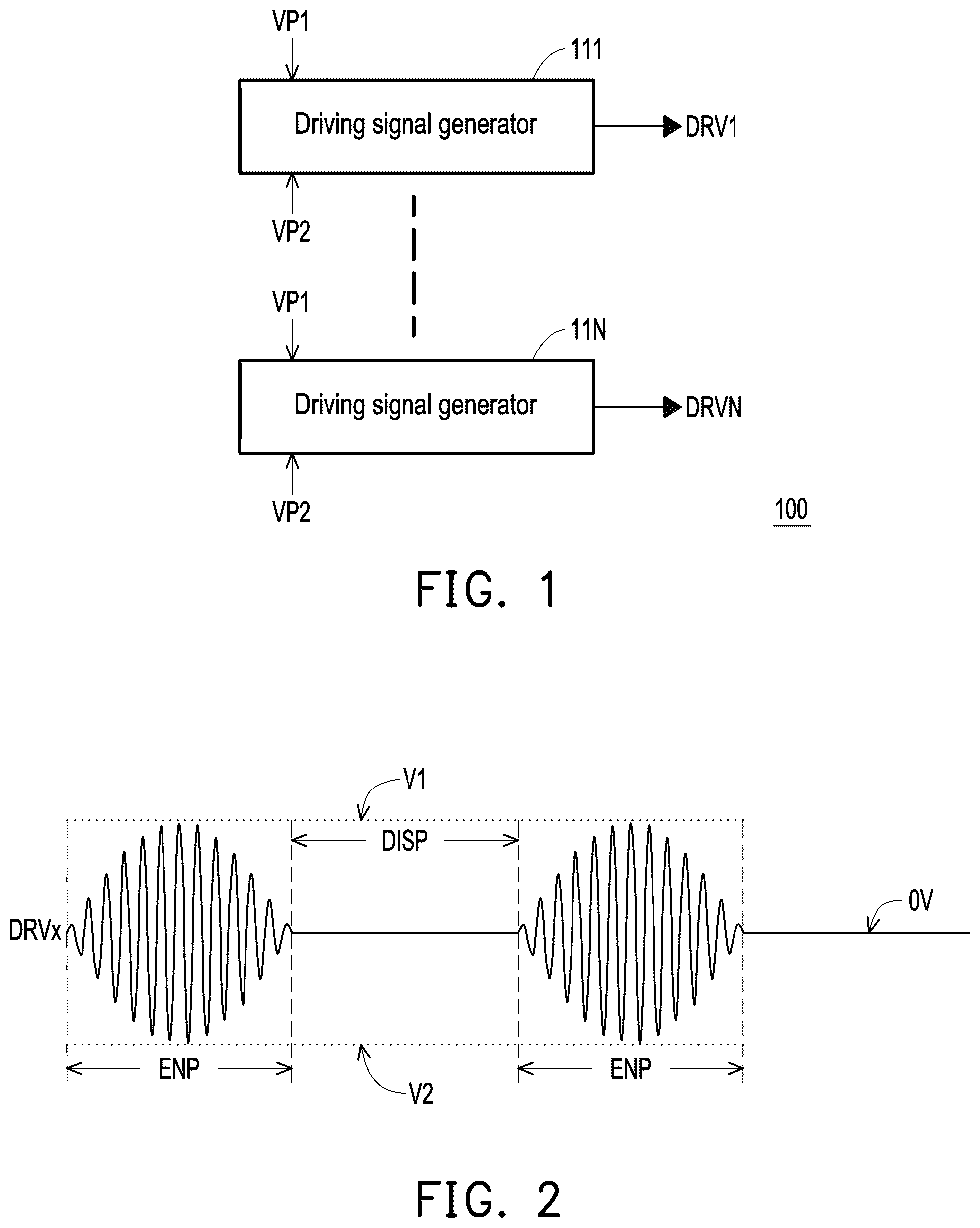
Please refer to , which illustrates a schematic diagram of a touch detection circuit according to an embodiment of present disclosure. The touch detection circuit 100 includes one or more driving signal generators 111 - 11 N and the driving signal generators 111 - 11 N respectively generates a plurality of driving signals DRV 1 -DRVN. The driving signal generators 111 - 11 N provides the driving signals DRV 1 -DRVN to a plurality of touch sensing pads for operating touch sensing operation. The touch sensing pads may be capacitive touch sensing pads.
In present embodiment, each of the driving signal generators 111 - 11 N receives a first power voltage VP 1 and a second power voltage VP 2 as operation voltages, wherein the first power voltage VP 1 may be larger than the second power voltage VP 2 . The first power voltage VP 1 is a positive power voltage, and the second power voltage VP 2 is a negative voltage. Furthermore, each of the driving signals DRV 1 -DRVN generated by each of the driving signal generators 111 - 11 N may swing between a first voltage and a second voltage, wherein the first voltage is a positive voltage and the second voltage is a negative voltage.
Please refer to and commonly, wherein illustrates a waveform plot of a driving signal generated by a driving signal generator according to an embodiment of present disclosure. In , the driving signal DRVx may be any one of the driving signals DRV 1 -DRVN, and may be generated by corresponding driving signal generator 11 x . When a touch sensing operation is activated, the driving signal generator 11 x may generates the driving signal DRVx with a sine wave during an enable period ENP. In this embodiment, the sine wave of the driving signal DRVx may swing between a first voltage V 1 and a second voltage V 2 , wherein the first voltage V 1 is larger than 0V, and the second voltage V 2 is smaller than 0V. Moreover, an amplitude of the sine wave of the driving signal DRVx can be modulated, and in this embodiment, the amplitude of the sine wave of the driving signal DRVx may be increased during a front half part of the enable period ENP, and the amplitude of the sine wave of the driving signal DRVx may be decreased during a back half part of the enable period ENP.
In this embodiment, an absolute value of the first power voltage VP 1 received by the driving signal generator 11 x is larger than an absolute value of the first voltage V 1 , and an absolute value of the second power voltage VP 2 received by the driving signal generator 11 x is larger than an absolute value of the second voltage V 2 . The absolute value of the first voltage V 1 and the second voltage V 2 may be same or different. The absolute value of the first power voltage VP 1 and the second power voltage VP 2 may be same or different, too.
On the other hand, when the touch sensing operation is not activated, the driving signal generator 11 x may generates the driving signal DRVx equal to 0V during a disable period DISP.
By generating the driving signal DRVx which transits between the first voltage VP 1 and the second voltage VP 2 , a frequency response diagram of the driving signal DRVx can be seen as . In , it can be seen that each magnitude of each of frequency spectrums below a frequency TXF of the driving signal DRVx is lower than a magnitude of frequency spectrum at the frequency TXF. That is, an interference of low frequency noise is reduced, and performance of a touch sensing device can be enhanced correspondingly.
It should be noted here, the frequency response diagram may be obtained by performing a Fast Fourier Transform (FFT) on the driving signal DRVx.
Please refer to , which illustrates a schematic diagram of a driving signal generator according to an embodiment of present disclosure. The driving signal generator 400 includes a first voltage buffer 411 , a second voltage buffer 412 , a signal converting circuit 420 and a third voltage buffer 430 . The first voltage buffer 411 is a voltage follower, and includes an operation amplifier OP 1 . A positive input end of the operation amplifier OP 1 receives a first input signal IN 1 and a negative input end of the operation amplifier OP 1 is coupled to an output end of the operation amplifier OP 1 . The operation amplifier OP 1 receives a first voltage VP 1 and aground voltage GND as operation powers.
The second voltage buffer 412 is also a voltage follower, and includes an operation amplifier OP 2 . A positive input end of the operation amplifier OP 2 receives a second input signal IN 2 and a negative input end of the operation amplifier OP 2 is coupled to an output end of the operation amplifier OP 2 . The operation amplifier OP 2 receives the ground voltage GND and a second voltage VP 2 as operation powers.
The first voltage buffer 411 is configure to receive the first input signal IN 1 , and generates a first voltage V 1 . The second voltage buffer 412 is configure to receive the second input signal IN 2 , and generates a first voltage V 2 . In this embodiment, the first voltage V 1 may be a positive voltage (larger than 0V), and the second voltage may be a negative voltage (smaller than 0V).
Besides, the signal converting circuit 420 is coupled to the output ends of the first voltage buffer 411 and the second voltage buffer 412 for respectively receiving the first voltage V 1 and the second voltage V 2 as power voltages. The signal converting circuit 420 further receives an input code CODE, and generates a converting signal CS 1 by converting the input code CODE.
In this embodiment, the signal converting circuit 420 may be a digital to analog converter (DAC), the input code CODE is a digital code, and the converting signal CS 1 is an analog signal.
The third voltage buffer 430 is coupled to the first voltage buffer 411 , the second voltage buffer 412 and the signal converting circuit 420 . The third voltage buffer 430 receives the first voltage V 1 and the second voltage V 2 as power voltages. The third voltage buffer 430 may be a voltage follower and includes an operation amplifier OP 3 . The operation amplifier OP 3 receives the converting signal CS 1 by a positive input end, and a negative input end and an output end of the operation amplifier OP 3 are coupled together. The operation amplifier OP 3 generates the driving signal DRV by the output end of the operation amplifier OP 3 , and the driving signal DRV may swing between the first voltage V 1 and the second voltage V 2 .
It should be noted here, amplitude of the driving signal DRV can be controlled by the input code CODE. A positive peak value of the driving signal DRV may be equal or less than the first voltage V 1 , and a negative peak value of the driving signal DRV may be equal or larger than the second voltage V 2 . The input code CODE may be a time varying code and an amplitude of the driving signal DRV can be modulated according to a variation of the input code CODE as the driving signal DRVx shown in .
In this embodiment, the first voltage V 1 may be 3V, and the first power voltage VP 1 may be 6V. The second voltage V 2 may be −3V, and the second power voltage VP 1 may be −6V. The first voltage V 1 may be half of the first power voltage VP 1 , and the second voltage V 2 may be half of the second power voltage VP 2 . Or in some embodiments, the first voltage V 1 may be the first power voltage VP 1 multiplied by N, the second voltage V 2 may be the second power voltage VP 2 multiplied by M, wherein N and M are positive real numbers smaller than 1, and N and M may be same or different.
Please refer to A , which illustrates a schematic diagram of a driving signal generator according to another embodiment of present disclosure. The driving signal generator 500 includes a first signal converting circuit 511 , a second signal converting circuit 512 , a first voltage buffer 521 , a second voltage buffer 522 and a multiplexer (Mux) 530 . The first signal converting circuit 511 and the second signal converting circuit 512 are digital to analog converter (DAC). The first signal converting circuit 511 receives a first input code IC 1 and converts the first input code IC 1 to generate a first converting signal CS 1 . The second signal converting circuit 512 receives a second input code IC 2 and converts the second input code IC 2 to generate a second converting signal CS 2 . The first voltage buffer 521 and the second voltage buffer 522 are respectively coupled to the first signal converting circuit 511 and the second signal converting circuit 512 . The first voltage buffer 521 receives the first converting signal CS 1 and generates a first buffering signal BS 1 . The second voltage buffer 522 receives the second converting signal CS 2 and generates a second buffering signal BS 2 .
In detail, the first voltage buffer 521 includes an operation amplifier OP 1 . The operation amplifier OP 1 receives a first power voltage VP 1 and a ground voltage GND as operation powers. The first power voltage VP 1 is a positive voltage. A positive input end of the operation amplifier OP 1 receives the first converting signal CS 1 , and a negative end of the operation amplifier OP 1 is coupled to an output end of the operation amplifier OP 1 . The first voltage buffer 521 is a voltage follower, and generates the buffering signal BS 1 according to the first converting signal CS 1 . In this embodiment, the buffering signal BS 1 may be kept on 0V in some time period or may be sine wave with an amplitude equal to a first voltage V 1 in some other time periods, wherein the first voltage V 1 is larger than 0V.
The second voltage buffer 521 includes an operation amplifier OP 2 . The operation amplifier OP 2 receives a second power voltage VP 2 and the ground voltage GND as operation powers. The second power voltage VP 2 is a negative voltage. A positive input end of the operation amplifier OP 2 receives the second converting signal CS 2 , and a negative end of the operation amplifier OP 2 is coupled to an output end of the operation amplifier OP 2 . The second voltage buffer 522 is also a voltage follower, and generates the buffering signal BS 2 according to the second converting signal CS 2 . In this embodiment, the buffering signal BS 2 may be kept on 0V in some time period or may be sine wave with an amplitude equal to a second voltage V 2 in some other time periods, wherein the second voltage V 2 is smaller than 0V.
It should be noted here, when the buffering signal BS 1 is kept on 0V, the buffering signal BS 2 is the sine wave with a negative amplitude, and when the buffering signal BS 2 is kept on 0V, the buffering signal BS 1 is the sine wave with a positive amplitude.
The multiplexer 530 is coupled to the first voltage buffer 521 and the second voltage buffer 522 . The multiplexer 530 generates a driving signal DRV by alternatively selecting one of the buffering signals BS 1 and BS 2 . In detail, during time periods ta, the multiplexer 530 selects the buffering signal BS 1 to generate the driving signal DRV, and during time periods tb, the multiplexer 530 selects the buffering signal BS 2 to generate the driving signal DRV. Such as that, the driving signal DRV may be a sine wave swing between the first voltage V 1 and the second voltage V 2 .
In additional, the voltage converting circuits 511 and 512 may be implemented by any digital to analog converter known by a person skilled in the art, and the multiplexer 530 also may be implemented by any signal multiplex circuit known by a person skilled in the art, no special limitation here.
Please refer to B , which illustrates a schematic diagram of a driving signal generator according to another embodiment of present disclosure. Different from the driving signal generator 500 in A , the driving signal generator 500 ′ B further includes a third signal converting circuit 513 , a fourth signal converting circuit 514 , a third voltage buffer 523 and a fourth voltage buffer 524 . The third signal converting circuit 513 and the fourth signal converting circuit 514 respectively generate converting signal CS 3 and CS 4 . The third voltage buffer 523 and the fourth voltage buffer 524 respectively receive the converting signal CS 3 and CS 4 , and respectively generate buffering signals BS 3 and BS 4 . The third voltage buffer 523 and the fourth voltage buffer 524 are both voltage followers. The third voltage buffer 523 and the fourth voltage buffer 524 are respectively formed by operation amplifiers OP 3 and OP 4 . Detail circuit structures of the first voltage buffer 521 to the fourth voltage buffer 524 are the same, and no more repeat description here.
In here, please refer to B and C commonly, wherein C is a waveform plot of the buffering signals of the driving signal generator 500 ′ of the embodiment of B . In C , during time periods ta, the buffering signal BS 1 is a sine wave with a positive amplitude; the buffering signal BS 2 is a sine wave with a negative amplitude; and the buffering signals BS 3 and BS 4 are kept on 0V. During time periods tb, the buffering signal BS 4 is a sine wave with a positive amplitude; the buffering signal BS 2 is a sine wave with a negative amplitude; and the buffering signals BS 1 and BS 2 are kept on 0V.
In this embodiment, there is a first phase difference between the buffering signal BS 1 and the buffering signal BS 3 ; there is a second phase difference between the buffering signal BS 2 and the buffering signal BS 4 ; and the first phase difference may be equal to the second phase difference.
Please refer to B again. In this embodiment, the multiplexer 530 receives the buffering signals BS 1 -BS 4 . The multiplexer 530 may alternatively select one of the buffering signals BS 1 and BS 2 to generate a driving signal DRV 1 , or the multiplexer 530 may alternatively select one of the buffering signals BS 3 and BS 4 to generate a driving signal DRV 2 , wherein there is a phase difference between the driving signal DRV 1 and the driving signal DRV 2 .
Please refer to , which illustrates a schematic plot of a touch sensing device according to an embodiment of present disclosure. The touch sensing device 600 may be applied on a touch display device. The touch sensing device 600 includes a touch detection circuit and a touch sensing array 630 . The touch sensing array 630 may be disposed overlapped with a display panel of the touch display device. The display panel may be a liquid crystal display (LCD) panel, a light emitting diode (LED) display panel, or a organic LED (OLED) display panel. The touch detection circuit includes a plurality of driving signal generators 611 - 61 N and a plurality of sensing signal receivers 621 - 62 M. In some embodiment, the touch detection circuit may be integrated with a display driver of the display panel to from a touch with display driver (TDDI) circuit.
The touch sensing array 630 includes a plurality of touch sensing pads TP, and the touch sensing pads TP are arranged in an array. Each of the driving signal generators 611 - 61 N corresponds to each of rows of the touch sensing array 630 , and each of the sensing signal receivers 621 - 62 M corresponds to each of columns of the touch sensing array 630 . Each of the driving signal generators 611 - 61 N generates driving signals to corresponding touch sensing pads TP, and the sensing signal receivers 621 - 62 M respectively receive a plurality of sensing signals generated by corresponding touch sensing pads based on the driving signals during a sensing period.
In this embodiment, the touch sensing pads TP are capacitive touch sensing pads.
Please refer to , which illustrates a waveform plot of driving signals of touch sensing device according to an embodiment of present disclosure. In this embodiment, the driving signal generators may be grouped into a plurality of signal generator groups, and each of the signal generator groups may include 4 driving signal generators, and the 4 driving signal generators may respectively generate driving signals DRV 1 to DRV 4 . In , one of the driving signals DRV 1 to DRV 4 may has a first phase and the others driving signals DRV 1 to DRV 4 may have a second phase during each of a plurality of touch sensing periods STP 1 -STP 4 , where the first phase is different from the second phase. In detail, during the touch sensing period STP 1 , the driving signal DRV 1 has a negative phase, and the driving signals DRV 2 -DRV 4 have a positive phase; during the touch sensing period STP 2 , the driving signal DRV 2 has the negative phase, and the driving signals DRV 1 , DRV 3 and DRV 4 have the positive phase; during the touch sensing period STP 3 , the driving signal DRV 3 has the negative phase, and the driving signals DRV 1 , DRV 2 and DRV 4 have the positive phase; and during the touch sensing period STP 4 , the driving signal DRV 4 has the negative phase, and the driving signals DRV 1 -DRV 3 have the positive phase.
Please refer to and commonly, wherein illustrates a schematic diagram for touch sensing operation according to an embodiment of present disclosure. In , during the touch sensing period STP 1 , the driving signals DRV 1 -DRV 4 with phases −, +, +, + can be transported to touch sensing pads TP 1 -TP 4 . A sensing signal receiver RX 1 corresponding to the touch sensing pads TP 1 -TP 4 can receive sensing signal w from the touch sensing pads TP 1 -TP 4 during the touch sensing period STP 1 . During the touch sensing period STP 2 , the driving signals DRV 1 -DRV 4 with phases +, −, +, + can be transported to touch sensing pads TP 1 -TP 4 . The sensing signal receiver RX 1 can receive sensing signal x from the touch sensing pads TP 1 -TP 4 during the touch sensing period STP 2 . During the touch sensing period STP 3 , the driving signals DRV 1 -DRV 4 with phases +, +, −, + can be transported to touch sensing pads TP 1 -TP 4 . The sensing signal receiver RX 1 can receive sensing signal y from the touch sensing pads TP 1 -TP 4 during the touch sensing period STP 3 . Moreover, during the touch sensing period STP 4 , the driving signals DRV 1 -DRV 4 with phases +, +, +, − can be transported to touch sensing pads TP 1 -TP 4 . The sensing signal receiver RX 1 can receive sensing signal z from the touch sensing pads TP 1 -TP 4 during the touch sensing period STP 4 . In this embodiment, the sensing signals w, x, y, z can be generated according to corresponding driving signals DRV 1 to DRV 4 and capacitance variation values a, b, c, d of the touch sensing pads TP 1 -TP 4 , respectively.
A relationship between the sensing signals w, x, y, z and the capacitance variation values a, b, c, d can be represented by a formulation shown as below:
[ - + + + + - + + + + - + + + + - ] = [ a b c d ] = [ w x y z ]
By expanding the matrix operation shown above, equation set can be obtained as below:
{ a = 1 4 ( - w + x + y + z ) b = 1 4 ( w - x + y + z ) c = 1 4 ( w + x - y + z ) d = 1 4 ( w + x + y - z )
Such as that, by the equation set shown above, the capacitance variation values a, b, c, d can be obtained, and touching information can be generated according to the capacitance variation values a, b, c, d.
It should be noted here, in this embodiment, one of the driving signals DRV 1 -DRV 4 is selected to have a different phase (the first phase). In some other embodiments, two or more of the driving signals DRV 1 -DRV 4 may be selected to has the first phase. Furthermore, one signal generator group may have two or more driving signal generators. The 4 driving signal generators in one signal generator group in present embodiment is just an example for illustration, and not limit an invention scope of present disclosure.
In summary, present disclosure provides the driving signal generator to generate the driving signal swing between a positive voltage and a negative voltage for touch sensing detection operation. Such as that a swing magnitude of the driving signal can be reduced and an interference by low frequency noise can be reduced, and performance of touch sensing operation can be enhanced, too.
Figures (9)
Citations
This patent cites (8)
- US2015/0261340
- US2018/0107309
- US2018/0188865
- US2021/0004103
- US2021/0191561
- US2021/0313401
- US2022/0326831
- US4365884