Sensor and Sensor System Including Multiple Detection Portions
Abstract
According to one embodiment, a sensor includes a detection device and a circuit portion. The detection device includes a first detection portion and a second detection portion. The first detection portion includes a first detection element. The first detection element includes a first conductive member and a first detection member. The second detection portion includes a second detection element. The second detection element includes a second conductive member and a second detection member. The circuit portion is configured to execute a first detection portion operation for outputting a first detection result corresponding to a first detection value based on the first detection member when a first current is supplied to the first conductive member. In a case where a first evaluation value is not within a first range, the circuit portion is configured to execute a second detection portion operation by the second detection portion.
Claims (20)
1. A sensor, comprising: a detection device including a first detection portion and a second detection portion; and a circuit portion, the first detection portion including a first detection element, the first detection element including a first conductive member and a first detection member, the second detection portion including a second detection element, the second detection element including a second conductive member and a second detection member, the circuit portion being configured to execute a first detection portion operation for outputting a first detection result corresponding to a first detection value based on the first detection member when a first current is supplied to the first conductive member, in a case where a first evaluation value is not within a first range, the circuit portion being configured to execute a second detection portion operation by the second detection portion, the first evaluation value including at least one of a value based on the first detection member when the first current is not supplied to the first conductive member or a value based on the first conductive member when the first current is substantially not supplied to the first conductive member.
Show 19 dependent claims
2. The sensor according to claim 1 , wherein the circuit portion is configured to further execute the first detection portion operation when the first evaluation value is within the first range.
3. The sensor according to claim 2 , wherein when the first detection portion operation is further performed, the circuit portion is configured to adjust at least one of the first current or a derivation condition of the first detection value based on the first evaluation value.
4. The sensor according to claim 1 , wherein in the second detection portion operation, the circuit portion is configured to output a second detection result corresponding to a second detection value based on the second detection member when a second current is supplied to the second conductive member, in a case where the second evaluation value is not within a second range, the circuit portion does not further execute the second detection portion operation, and the second evaluation value includes at least one of a value based on the second detection member when the second current is not supplied to the second conductive member or a value based on the second conductive member when the second current is substantially not supplied to the second conductive member.
5. The sensor according to claim 4 , wherein the circuit portion is configured to output information including a warning in a case where the second evaluation value is not within the second range.
6. The sensor according to claim 4 , wherein the circuit portion is configured to further execute the second detection portion operation when the second evaluation value is within the second range.
7. The sensor according to claim 4 , wherein the circuit portion includes a switch circuit, the switch circuit is configured to switch between supplying the first current to the first conductive member and not supplying the first current to the first conductive member, and the switch circuit is configured to switch between supplying the second current to the second conductive member and not supplying the second current to the second conductive member.
8. The sensor according to claim 7 , wherein the circuit portion further includes a detection circuit, the detection circuit is configured to output the first detection result, and the detection circuit is configured to output the second detection result.
9. The sensor according to claim 8 , wherein the circuit portion further includes an evaluation circuit, the evaluation circuit is configured to output a first evaluation result as to whether or not the first evaluation value is within the first range, and the evaluation circuit is configured to output a second evaluation result as to whether the second evaluation value is within the second range.
10. The sensor according to claim 9 , wherein the circuit portion further includes a control circuit, and the control circuit is configured to control the switch circuit.
11. The sensor according to claim 9 , wherein the first detection member includes a first fixed electrode and a first movable electrode, the first detection portion includes a first reference element, the first reference element includes a first fixed reference electrode and a first movable reference electrode, and the first detection value is based on a difference between a first capacitance between the first fixed electrode and the first movable electrode when the first current is supplied to the first conductive member and a first reference capacitance between the first fixed reference electrode and the first movable reference electrode.
12. The sensor according to claim 11 , wherein the first capacitance is configured to change depending on a detection object around the first detection element, the first reference capacitance does not change depending on the detection object, or a first change rate of the first capacitance with respect to a change of the detection object is higher than a first reference change rate of the first reference capacitance with respect to the change of the detection object.
13. A sensor system, comprising: the sensor according to claim 9 ; and a control circuit, the control circuit being configured to control the switch circuit.
14. The sensor according to claim 8 , wherein the first detection portion includes a first reference element, the first reference element includes a first reference resistance member, the first detection member includes a first resistance member, and the first detection value is based on a difference between a first electrical resistance of the first resistance member when the first current is supplied to the first conductive member and a first reference electrical resistance of the first reference resistance member.
15. The sensor according to claim 14 , wherein the first detection portion further includes a base body, and a first support portion fixed to the base body, the first detection element is supported by the first support portion, and a first gap is provided between the base body and the first detection element.
16. The sensor according to claim 15 , wherein the first electrical resistance is configured to change depending on a detection object around the first detection element.
17. The sensor according to claim 16 , wherein the first reference electrical resistance does not change depending on the detection object, or a first rate of a change of the first electrical resistance with respect to a change of the detection object is higher than a first reference rate of a change of the first reference electrical resistance with respect to the change of the detection object.
18. The sensor according to claim 16 , wherein the detection object includes at least one selected from the group consisting of carbon dioxide, carbon monoxide, hydrogen, helium, argon, carbon monoxide, carbon dioxide, methane, propane, butane, sulfur hexafluoride, nitrogen, oxygen, ammonia, acetone, chlorine, and alcohol.
19. The sensor according to claim 1 , wherein the first detection member includes a first resistance member, and the first detection result is a first electrical resistance of the first resistance member.
20. A sensor system, comprising: the sensor according to claim 1 ; and a control circuit configured to control the circuit portion.
Full Description
Show full text →
CROSS-REFERENCE TO RELATED APPLICATIONS
This application is based upon and claims the benefit of priority from Japanese Patent Application No. 2022-146147, filed on Sep. 14, 2022; the entire contents of which are incorporated herein by reference.
FIELD
Embodiments described herein generally relate to a sensor and sensor system.
BACKGROUND
For example, there are sensors using MEMS (Micro Electro Mechanical Systems) elements. Stable detection is desired in the sensor.
BRIEF DESCRIPTION OF THE DRAWINGS
is a schematic diagram illustrating a sensor according to a first embodiment;
is a flowchart illustrating the operation of the sensor according to the first embodiment;
is a schematic diagram illustrating a part of the sensor according to the first embodiment;
is a schematic diagram illustrating a part of the sensor according to the first embodiment;
is a schematic diagram illustrating a part of the sensor according to the first embodiment;
is a schematic diagram illustrating a part of the sensor according to the first embodiment;
is a schematic diagram illustrating the operation of the sensor according to the first embodiment;
is a schematic diagram illustrating the operation of the sensor according to the first embodiment;
is a schematic cross-sectional view illustrating a part of the sensor according to the first embodiment;
A and 10 B are schematic cross-sectional views illustrating a part of the sensor according to the first embodiment;
is a schematic plan view illustrating a part of the sensor according to the first embodiment;
A and 12 B are schematic plan views illustrating a part of the sensor according to the first embodiment; and
is a schematic cross-sectional view illustrating a part of a sensor according to the first embodiment.
DETAILED DESCRIPTION
According to one embodiment, a sensor includes a detection device and a circuit portion. The detection device includes a first detection portion and a second detection portion. The first detection portion includes a first detection element. The first detection element includes a first conductive member and a first detection member. The second detection portion includes a second detection element. The second detection element includes a second conductive member and a second detection member. The circuit portion is configured to execute a first detection portion operation for outputting a first detection result corresponding to a first detection value based on the first detection member when a first current is supplied to the first conductive member. In a case where a first evaluation value is not within a first range, the circuit portion is configured to execute a second detection portion operation by the second detection portion. The first evaluation value includes at least one of a value based on the first detection member when the first current is not supplied to the first conductive member or a value based on the first conductive member when the first current is substantially not supplied to the first conductive member.
Various embodiments are described below with reference to the accompanying drawings.
The drawings are schematic and conceptual; and the relationships between the thickness and width of portions, the proportions of sizes among portions, etc., are not necessarily the same as the actual values. The dimensions and proportions may be illustrated differently among drawings, even for identical portions.
In the specification and drawings, components similar to those described previously or illustrated in an antecedent drawing are marked with like reference numerals, and a detailed description is omitted as appropriate.
First Embodiment
is a schematic diagram illustrating a sensor according to the first embodiment.
is a flowchart illustrating the operation of the sensor according to the first embodiment.
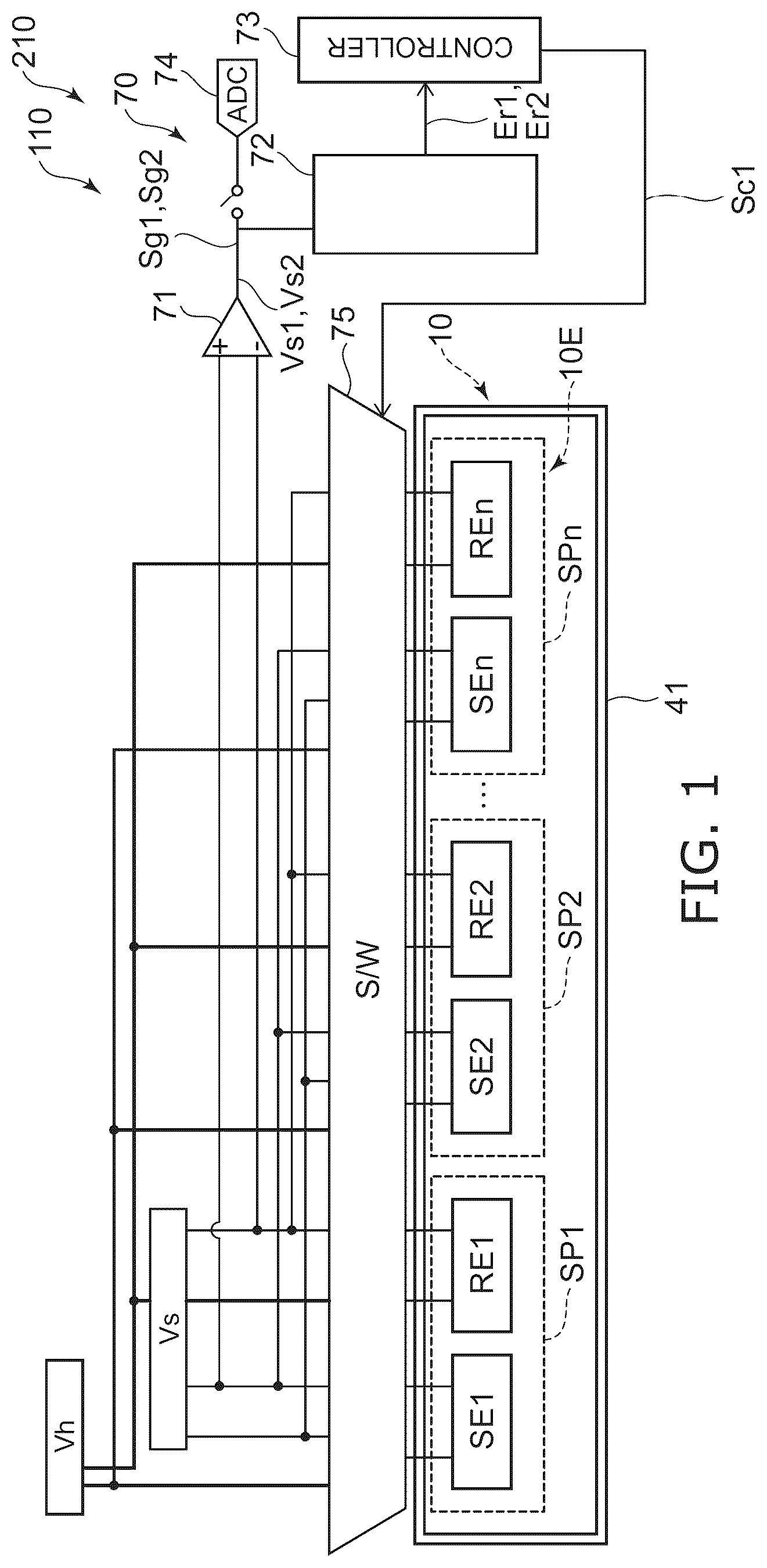
As shown in , a sensor 110 according to the embodiment includes a detection device 10 and a circuit portion 70 . The detection device 10 includes a plurality of detection portions 10 E. The plurality of detection portions 10 E include a first detection portion SP 1 , a second detection portion SP 2 , an n-th detection portion SPn, and the like. “n” is an integer of 2 or greater.
As shown in , the first detection portion SP 1 includes a first detection element SE 1 . The first detection element SE 1 includes a first conductive member CM 1 and a first detection member SM 1 (see ). As shown in , the second detection portion SP 2 includes a second detection element SE 2 . The second detection element SE 2 includes a second conductive member CM 2 and a second detection member SM 2 (see ). As shown in , the n-th detection portion SPn includes an n-th detection element SEn. The n-th detection element SEn includes an n-th conductive member and an n-th detection member.
illustrates an operation executed by the circuit portion 70 . As shown in , the circuit portion 70 is configured to execute the first detection portion operation S 110 . In the first detection portion operation S 110 , the circuit portion 70 is configured to execute the first detection operation S 111 . In the first detection operation S 111 , the circuit portion 70 outputs a first detection result Sg 1 (see ) corresponding to a first detection value Vs 1 (see ) based on the first detection member SM 1 when a first current is supplied to the first conductive member CM 1 . The first detection operation S 111 corresponds to the detection operation of the detection object using the first detection portion SP 1 .
As shown in , the circuit portion 70 executes a first evaluation operation S 112 , which will be described later. By the first evaluation operation S 112 , the first evaluation value Ve 1 is derived.
As shown in , the circuit portion 70 executes a first determination operation S 113 for determining whether or not the first evaluation value Ve 1 is within a first range. For example, a first evaluation value Ve 1 is compared with a lower threshold value Vth_L and a higher threshold value Vth_H.
In the case where the first evaluation value Ve 1 is not within the first range, the circuit portion 70 is configured to execute the second detection portion operation S 120 by the second detection portion SP 2 . The case where the first evaluation value Ve 1 is not within the first range corresponds to the case where the first detection portion SP 1 is not normal. In this case, the detection operation is executed by switching from the first detection portion SP 1 to the second detection portion SP 2 . As a result, detection by the detection portion 10 E which is not normal is not executed. The detection is switched to the detection portion 10 E being normal (second detection portion SP 2 ). According to an embodiment, a sensor capable of stable detection can be provided.
For example, by supplying the first current to the first conductive member CM 1 , the characteristics (e.g., electrical resistance) of the first conductive member CM 1 is changed. By supplying the first current to the first conductive member CM 1 , the temperature of the first detection member SM 1 is increased. As a result, the characteristics of the first detection member SM 1 is changed. The characteristic of the first detection member SM 1 includes, for example, a rate of change of the electrical resistance of the first detection member SM 1 by the detection object. The characteristic of the first detection member SM 1 includes, for example, a rate of change in shape of the first detection member SM 1 by the detection object. The characteristic of the first detection member SM 1 includes, for example, a rate of change in volume of the first detection member SM 1 by the detection object. Thus, there is a case where by supplying the first current to the first conductive member CM 1 , the characteristics of the first detection portion SP 1 is changed and the first detection portion SP 1 may have difficulty in normal detection. For example, a failure would occur in the first detection portion SP 1 . For example, the lifetime of the first detection portion SP 1 would end. In the embodiment, detection by the detection portion 10 E which is not normal is not executed. A sensor capable of stable detection can be provided.
In the first determination operation S 113 , if the first evaluation value Ve 1 is within the first range, the circuit portion 70 is configured to further execute the first detection portion operation S 110 (the first detection operation S 111 ). For example, in the case where the first detection portion SP 1 is normal, the first detection operation S 111 by the first detection portion SP 1 may be repeated.
The first evaluation value Ve 1 may include, for example, a value (first detection member evaluation value) based on the first detection member SM 1 when the first current is not supplied to the first conductive member CM 1 . The first evaluation value Ve 1 may include, for example, a value based on the first conductive member CM 1 when the first current is not substantially supplied to the first conductive member CM 1 (the first conductive member evaluation value). The first evaluation value Ve 1 may include, for example, at least one of the first detection member evaluation value and the first conductive member evaluation value.
In the embodiment, the detection object is detected by the detection value when the current is supplied to the conductive member. Normal and abnormal conditions of the first detection portion SP 1 are detected by the evaluation value when no current is supplied to the conductive member.
As shown in , in the second detection portion operation S 120 , the circuit portion 70 is configured to execute the second detection operation S 121 . In the second detection operation S 121 , the circuit portion 70 is configured to output a second detection result Sg 2 (see ) corresponding to the second detection value Vs 2 (see ) based on the second detection member SM 2 when the second current is supplied to the second conductive member CM 2 . The second detection operation S 121 corresponds to the detection operation of the detection object using the second detection portion SP 2 . The second current may be the same as the first current.
As shown in , the circuit portion 70 executes a second evaluation operation S 122 , which will be described later. A second evaluation value Ve 2 is derived by the second evaluation operation S 122 .
As shown in , the circuit portion 70 executes a second determination operation S 123 of determining whether the second evaluation value Ve 2 is within the second range. For example, the second evaluation value Ve 2 is compared with the lower threshold value Vth_L and the higher threshold value Vth_H. The second range may be the same as the first range.
In the case where the second evaluation value Ve 2 is not within the second range, the circuit portion 70 does not further execute the second detection portion operation S 120 . The case where the second evaluation value Ve 2 is not within the second range corresponds to the case where the second detection portion SP 2 is not normal. In this case, the circuit portion 70 terminates the detection operation by the second detection portion SP 2 , for example. As a result, detection by the detection portion 10 E which is not normal is not executed. According to the embodiment, a sensor capable of stable detection can be provided.
As shown in , in the case where the second evaluation value Ve 2 is not within the second range, the circuit portion 70 may execute information output operation S 125 of outputting information including warning.
As shown in , the circuit portion 70 may be configured to execute a third detection operation S 130 by a third detection portion in the case where the second evaluation value Ve 2 is not within the second range. The third detection portion is another one of the plurality of detection portions 10 E. The third detection portion may be, for example, the n-th detection portion SPn. Stable detection is possible.
The circuit portion 70 may further execute the second detection portion operation S 120 when the second evaluation value Ve 2 is within the second range in the second determination operation S 123 . For example, when the second detection portion SP 2 is normal, the second detection operation S 121 by the second detection portion SP 2 may be repeatedly executed.
The second evaluation value Ve 2 may include, for example, a value (second detection member evaluation value) based on the second detection member SM 2 when the second current is not supplied to the second conductive member CM 2 . The second evaluation value Ve 2 may include, for example, a value (second conductive member evaluation value) based on the second conductive member CM 2 when the second current is not substantially supplied to the second conductive member CM 2 . The second evaluation value Ve 2 may include, for example, at least one of the second detection member evaluation value and the second conductive member evaluation value.
As shown in , circuit portion 70 may include a switch circuit 75 . The switch circuit 75 is configured to switch between supplying the first current to the first conductive member CM 1 and not supplying the first current to the first conductive member CM 1 . The switch circuit 75 is configured to switch between supplying the second current to the second conductive member CM 2 and not supplying the second current to the second conductive member CM 2 .
As shown in , the circuit portion 70 may further include a detection circuit 71 . The detection circuit 71 is configured to output the first detection result Sg 1 . As already explained, the first detection result Sg 1 is the value based on the first detection member SM 1 when the first current is supplied to the first conductive member CM 1 . The detection circuit 71 is configured to output the second detection result Sg 2 . As already explained, the second detection result Sg 2 is the value based on the second detection member SM 2 when the second current is supplied to the second conductive member CM 2 .
In this example, the circuit portion 70 includes an AD converter 74 . The first detection result Sg 1 and the second detection result Sg 2 are AD-converted. The output of the AD converter 74 may be used as the detection result of the detection object.
As shown in , circuit portion 70 may further include an evaluation circuit 72 . The evaluation circuit 72 is configured to output a first evaluation result Er 1 regarding whether the first evaluation value Ve 1 is within the first range. The evaluation circuit 72 is configured to output a second evaluation result Er 2 regarding whether the second evaluation value Ve 2 is within the second range.
The evaluation circuit 72 is, for example, a fault detection circuit. The evaluation circuit 72 may include, for example, a comparator. The evaluation circuit 72 may include, for example, an AD converter.
As shown in , the circuit portion 70 may further include a control circuit 73 . The control circuit 73 is configured to control the switch circuit 75 . For example, the first evaluation result Er 1 is supplied to the control circuit 73 . For example, the second evaluation result Er 2 is supplied to the control circuit 73 . The control circuit 73 supplies the switch circuit 75 with the first control signal Sc 1 based on these evaluation results. The switch circuit 75 is controlled by the first control signal Sc 1 .
As shown in , a conductive member power source Vh may be provided. The first current and the second current are supplied by the conductive member power source Vh. As shown in , a detection power source Vs may be provided. The first detection value Vs 1 , a second detection value Vs 2 , a first detection member evaluation value, and a second detection member evaluation value are obtained from the detection power source Vs. At least one of the conductive member power source Vh or the detection power source Vs may be included in the circuit portion 70 .
As shown in , in this example, the first detection portion SP 1 includes a first reference element RE 1 in addition to the first detection element SE 1 . The second detection portion SP 2 includes a second reference element RE 2 in addition to the second detection element SE 2 . The n-th detection portion SPn includes an n-th reference element REn in addition to the n-th detection element SEn. By detecting the characteristics of the detection element and the characteristics of the reference element, the detection object can be detected with high accuracy.
As shown in , the plurality of detection portion 10 E (first detection portion SP 1 , second detection portion SP 2 , n-th detection portion SPn, etc.) may be provided on a base body 41 .
is a schematic diagram illustrating a part of the sensor according to the first embodiment.
As shown in , the first detection element SE 1 includes the first conductive member CM 1 and the first detection member SM 1 . In this example, the first detection member SM 1 includes a first resistance member 11 . In this case, the first detection result Sg 1 is a first electrical resistance of the first resistance member 11 .
As shown in , the first detection portion SP 1 includes the first reference element RE 1 . The first reference element RE 1 includes a first reference resistance member SR 1 . In this example, the first reference element RE 1 includes a first reference conductive member CR 1 . The configuration of the first reference element RE 1 is the same as the configuration of the first detection element SE 1 . As a result, the reference operation with higher accuracy can be performed.
corresponds to the first detection operation S 111 . In the first detection operation S 111 , the first current i 1 based on the conductive member power source Vh is supplied to the first conductive member CM 1 . In the first detection operation S 111 , the conductive member power source Vh is not connected to the first reference conductive member CR 1 . In the first detection operation S 111 , the first current i 1 is not supplied to the first reference conductive member CR 1 . This operation is performed by the switch circuit 75 .
By the operation of the switch circuit 75 , the detection power source Vs is connected to the first resistance member 11 and the first reference resistance member SR 1 . The potential of the first resistance member 11 and the potential of the first reference resistance member SR 1 are supplied to the detection circuit 71 . The detection circuit 71 is, for example, a differential amplifier. The detection circuit 71 outputs a signal corresponding to the difference between these potentials as the first detection result Sg 1 .
The first detection value Vs 1 is based on a difference between the first electrical resistance of the first resistance member 11 when the first current i 1 is supplied to the first conductive member CM 1 and a first reference electrical resistance of the first reference resistance member SR 1 .
is a schematic diagram illustrating a part of the sensor according to the first embodiment.
corresponds to the first evaluation operation S 112 . In the first evaluation operation S 112 , the conductive member power source Vh is not connected to the first conductive member CM 1 (and the first reference conductive member CR 1 ). In the first evaluation operation S 112 , the first current i 1 is not supplied to the first conductive member CM 1 . This operation is performed by the switch circuit 75 .
The detection power source Vs is connected to the first resistance member 11 and the first reference resistance member SR 1 . The potential of the first resistance member 11 and the potential of the first reference resistance member SR 1 are supplied to the detection circuit 71 . The detection circuit 71 is, for example, a differential amplifier. A signal corresponding to the difference between these potentials are output from the detection circuit 71 . This signal corresponds to the first evaluation value Ve 1 .
As shown in , the evaluation circuit 72 compares the first evaluation value Ve 1 with the lower threshold Vth_L and the higher threshold Vth_H. The evaluation circuit 72 outputs the first evaluation result Er 1 .
The control circuit 73 supplies the switch circuit 75 with the first control signal Sc 1 based on the first evaluation result Er 1 . The switch circuit 75 is controlled by the first control signal Sc 1 . The control circuit 73 may output an information Sal including a warning.
is a schematic diagram illustrating a part of the sensor according to the first embodiment.
As shown in , the second detection element SE 2 includes the second conductive member CM 2 and the second detection member SM 2 . In this example, the second detection member SM 2 includes a second resistance member 12 . In this case, the second detection result Sg 2 is a second electrical resistance of the second resistance member 12 .
As shown in , the second detection portion SP 2 includes the second reference element RE 2 . The second reference element RE 2 includes a second reference resistance member SR 2 . In this example, the second reference element RE 2 includes a second reference conductive member CR 2 .
corresponds to the second detection operation S 121 . In the second detection operation S 121 , the second current i 2 based on the conductive member power source Vh is supplied to the second conductive member CM 2 . In the second detection operation S 121 , the conductive member power source Vh is not connected to the second reference conductive member CR 2 . This operation is performed by the switch circuit 75 .
By the operation of the switch circuit 75 , the detection power source Vs is connected to the second resistance member 12 and the second reference resistance member SR 2 . The potential of the second resistance member 12 and the potential of the second reference resistance member SR 2 are supplied to the detection circuit 71 . The detection circuit 71 outputs a signal corresponding to the difference between these potentials as the second detection result Sg 2 .
The second detection value Vs 2 is based on a difference between the second electrical resistance of the second resistance member 12 when the second current i 2 is supplied to the second conductive member CM 2 and a second reference electrical resistance of the second reference resistance member SR 2 .
is a schematic diagram illustrating a part of the sensor according to the first embodiment.
corresponds to the second evaluation operation S 122 . In the second evaluation operation S 122 , the conductive member power source Vh is not connected to the second conductive member CM 2 (and the second reference conductive member CR 2 ). In the second evaluation operation S 122 , the second current i 2 is not supplied to the second conductive member CM 2 . This operation is performed by the switch circuit 75 .
The detection power source Vs is connected to the second resistance member 12 and the second reference resistance member SR 2 . The potential of the second resistance member 12 and the potential of the second reference resistance member SR 2 are supplied to the detection circuit 71 . A signal corresponding to the difference between these potentials is output from the detection circuit 71 . This signal corresponds to the second evaluation value Ve 2 .
As shown in , the evaluation circuit 72 compares the second evaluation value Ve 2 with the lower threshold value Vth_L and the higher threshold value Vth_H. The second evaluation result Er 2 is output from the evaluation circuit 72 .
The control circuit 73 supplies the switch circuit 75 with the first control signal Sc 1 based on the second evaluation result Er 2 . The switch circuit 75 is controlled by the first control signal Sc 1 . The control circuit 73 may output the information Sal including the warning.
In the embodiments, the first reference conductive member CR 1 may be omitted. In the embodiments, the second reference conductive member CR 2 may be omitted.
are schematic diagrams illustrating the operation of the sensor according to the first embodiment.
corresponds to the first detection portion operation S 110 . corresponds to the second detection portion operation S 120 . The above operations may be sequentially performed for three or more detection portions 10 E.
As shown in , the control circuit 73 may be configured to supply a second control signal Sc 2 to at least one of the conductive member power source Vh or the detection power source Vs. The second control signal Sc 2 is based on at least one of the first evaluation result Er 1 or the second evaluation result Er 2 .
For example, when the first detection portion operation S 110 is further performed, the circuit portion 70 may adjust at least one of the first current i 1 or the deriving condition of the first detection value Vs 1 based on the first evaluation value Ve 1 . The first current i 1 may be adjusted, for example, by adjusting the conductive member power source Vh. The condition for deriving the first detection value Vs 1 may be adjusted by adjusting the detection power source Vs.
For example, when the second detection portion operation S 120 is further performed, the circuit portion 70 may adjust at least one of the second current i 2 or the derivation condition of the second detection value Vs 2 based on the second evaluation value Ve 2 . The second current i 2 may be adjusted, for example, by adjusting the conductive member power source Vh. The condition for deriving the second detection value Vs 2 may be adjusted by adjusting the detection power source Vs.
Examples of the detection device 10 are described below.
, 10 A and 10 B are schematic cross-sectional views illustrating a part of the sensor according to the first embodiment.
is a schematic plan view illustrating a part of the sensor according to the first embodiment.
is a cross-sectional view taken along the line A 1 -A 2 of . A is a cross-sectional view along the line B 1 -B 2 of . B is a cross-sectional view taken along the line C 1 -C 2 of . These figures show an example of the first detection portion SP 1 .
As shown in , 10 A, 10 B and 11 , the detection device 10 includes the first detection portion SP 1 . As already explained, the first detection portion SP 1 includes the first detection element SE 1 and the first reference element RE 1 . The first detection element SE 1 includes the first conductive member CM 1 and the first detection member SM 1 . In this example, the first reference element RE 1 includes the first reference resistance member SR 1 and the first reference conductive member CR 1 . In this example, the first detection member SM 1 includes the first resistance member 11 .
In this example, the first detection portion SP 1 includes the base body 41 . The base body 41 includes a first base region 41 a and a second base region 41 b . The first detection element SE 1 is provided at the first base region 41 a . The first reference element RE 1 is provided at the second base region 41 b.
In this example, the first base region 41 a is continuous with the second base region 41 b . The boundary between the first base region 41 a and the second base region 41 b may be clear or unclear. The first base region 41 a may be separated from the second base region 41 b.
In this example, the base body 41 includes a substrate 41 s and an insulating film 41 i . The substrate 41 s may be, for example, a semiconductor substrate (for example, a silicon substrate). The substrate 41 s may include, for example, a semiconductor circuit. The substrate 41 s may include connecting members such as via electrodes.
A direction from the first base region 41 a to the first detection element SE 1 is defined as a Z-axis direction. One direction perpendicular to the Z-axis direction is defined as an X-axis direction. The direction perpendicular to the Z-axis direction and the X-axis direction is defined as a Y-axis direction. The direction from the second base region 41 b to the first reference element RE 1 is along the Z-axis direction.
In this example, the first detection portion SP 1 further includes a first connection portion 31 C and a first support portion 31 S. The first support portion 31 S is fixed to the base body 41 . A part of the first connection portion 31 C is supported by the first support portion 31 S. Another part of the first connection portion 31 C supports the first detection element SE 1 to be away from the first base region 41 a . A first gap g 1 is provided between the first base region 41 a and the first detection element SE 1 .
In this example, the first detection portion SP 1 includes a first reference connection portion 31 RC and a first reference support portion 31 RS. The first reference support portion 31 RS is fixed to the base body 41 . A part of the first reference connection portion 31 RC is supported by the first reference support portion 31 RS. Another part of the first reference connection portion 31 RC supports the first reference element RE 1 to be away from the second base region 41 b . A second gap g 2 is provided between the second base region 41 b and the first reference element RE 1 .
By the first detection element SE 1 and the first reference element RE 1 being supported to be away from the base body 41 , conduction of heat from these elements via the base body 41 is suppressed. As a result, stable detection of the detection object with high sensitivity can be performed.
As shown in , the first detection element SE 1 may include a first insulating portion 18 . The first reference element RE 1 may include a first reference insulating portion 18 R. At least part of the first insulating portion 18 is provided around the first resistance member 11 (first detection member SM 1 ) and the first conductive member CM 1 . At least part of the first reference insulating portion 18 R is provided around the first reference resistance member SR 1 and the first reference conductive member CR 1 .
A and 12 B are schematic plan views illustrating a part of the sensor according to the first embodiment.
These figures are plan views relating to a layer including the first detection member SM 1 (first resistance member 11 ) and the first reference resistance member SR 1 . As shown in A, the first detection element SE 1 may include a first layer 15 a and a second layer 15 b . The first layer 15 a and the second layer 15 b have the same material and thickness as those of the first resistance member 11 . The first resistance member 11 is provided between the first layer 15 a and the second layer 15 b . By providing these layers, warpage (deformation) of the first detection element SE 1 is suppressed.
As shown in B , the first reference element RE 1 may include a third layer 15 c and a fourth layer 15 d . The third layer 15 c and the fourth layer 15 d have the same material and thickness as those of the first reference resistance member SR 1 . The first reference resistance member SR 1 is provided between the third layer 15 c and the fourth layer 15 d . Warping (deformation) of the first reference resistance member SR 1 is suppressed by providing these layers.
Thus, the first detection portion SP 1 may include the base body 41 and the first support portion 31 S fixed to the base body 41 . The first detection element SE 1 is supported by the first support portion 31 S. The first gap g 1 is provided between the base body 41 and the first detection element SE 1 .
The first electrical resistance of the first resistance member 11 (first detection member SM 1 ) can be changed according to the detection object around the first detection element SE 1 . For example, by supplying a current to the first conductive member CM 1 , the temperature of the first detection element SE 1 rises, and then the temperature drops. The degree of heat dissipation of the first detection element SE 1 varies depending on the detection object. For example, the temperature of the first detection element SE 1 changes depending on the detection object. The characteristics of the first detection member SM 1 (for example, the first resistance member 11 ) change with the change in temperature. For example, the first electrical resistance of the first resistance member 11 depends on the detection object. The detection object can be detected by detecting a value based on the first electrical resistance. The sensor 110 is a resistance detection type sensor.
The first reference electrical resistance of the first reference resistance member SR 1 does not substantially change according to the detection object. Alternatively, a first rate of change of the first electrical resistance with respect to the change of the detection object is higher than a first reference rate of change of the first reference electrical resistance with respect to the change of the detection object.
In the embodiments, the detection object may be gas or liquid. The detection object includes, for example, at least one selected from the group consisting of hydrogen, helium, argon, carbon monoxide, carbon dioxide, methane, propane, butane, and sulfur hexafluoride (SF 6 ). The detection object may include, for example, at least one selected from the group consisting of nitrogen, oxygen, ammonia, acetone, and chlorine (Cl 2 ). The detection object may include, for example, alcohol.
is a schematic cross-sectional view illustrating a part of a sensor according to the first embodiment.
illustrates the first detection portion SP 1 in a sensor 120 according to the embodiment. Also in the sensor 120 , the first detection portion SP 1 includes the first detection element SE 1 and the first reference element RE 1 . The first detection element SE 1 includes the first conductive member CM 1 and the first detection member SM 1 . In this example, the first reference element RE 1 includes the first reference resistance member SR 1 and the first reference conductive member CR 1 . In the sensor 120 , the first detection member SM 1 includes a first fixed electrode 11 F and a first movable electrode 11 A. The first reference element RE 1 includes a first fixed reference electrode 11 RF and a first movable reference electrode 11 RA. The configuration of the sensor 120 except for this may be the same as the configuration of the sensor 110 .
The sensor 120 is a capacitance detection type sensor. The sensor 120 detects a first capacitance Cs 1 between the first fixed electrode 11 F and the first movable electrode 11 A. A first reference capacitance Cr 1 between the first fixed reference electrode 11 RF and the first movable reference electrode 11 RA is detected. A difference between the first capacitance Cs 1 and the first reference capacitance Cr 1 is derived.
For example, in the first detection element SE 1 , the detection object is taken into a layer included in the first detection element SE 1 . As a result, the layers included in the first detection element SE 1 is deformed. As the distance between the first fixed electrode 11 F and the first movable electrode 11 A changes, the first capacitance Cs 1 changes. By supplying a current to the first conductive member CM 1 included in the first detection element SE 1 , the temperature of the first detection element SE 1 rises, and the degree to which the detection object is taken in increases, for example.
On the other hand, the temperature of the first reference element RE 1 does not rise. The shape of the first reference element RE 1 does not substantially change even if the detection object changes. Therefore, the first reference capacitance Cr 1 does not substantially change even if the detection object changes. By detecting the difference between the first capacitance Cs 1 and the first reference capacitance Cr 1 , the detection object can be detected with high accuracy.
In the sensor 120 , the first detection value Vs 1 is based on the difference between the first capacitance Cs 1 between the first fixed electrode 11 F and the first movable electrode 11 A when the first current i 1 is supplied to the first conductive member CM 1 , and the first reference capacitance Cr 1 between the first fixed reference electrode 11 RF and the first movable reference electrode 11 RA.
The first capacitance Cs 1 can be changed according to the detection object around the first detection element SE 1 . The first reference capacitance Cr 1 does not change depending on the detection object. Alternatively, the first rate of change of the first capacitance Cs 1 with respect to the change of the detection object is higher than the first reference rate of change of the first reference capacitance Cr 1 with respect to the change of the detection object.
Second Embodiment
The second embodiment relates to a sensor system. The sensor system 210 according to the embodiment includes the sensor according to the first embodiment (e.g., the sensor 110 or the sensor 120 ) and the control circuit 73 (see ). The control circuit 73 is configured to control the circuit portion 70 (for example, the switch circuit 75 ). The control circuit 73 may be configured to control at least one of the detection circuit 71 or the evaluation circuit 72 . The control circuit 73 may be configured to control at least one of the conductive member power source Vh or the detection power source Vs.
The control circuit 73 may be provided at a location different from the location where the detection device 10 and the switch circuit 75 are provided. The control circuit 73 may be configured to communicate with the sensor according to the first embodiment by any wired or wireless method. The control circuit 73 may include a computer.
Embodiments may include the following configurations (e.g., technical proposals).
Configuration 1
A sensor, comprising:
•
• a detection device including a first detection portion and a second detection portion; and • a circuit portion, • the first detection portion including a first detection element, the first detection element including a first conductive member and a first detection member, • the second detection portion including a second detection element, the second detection element including a second conductive member and a second detection member, • the circuit portion being configured to execute a first detection portion operation for outputting a first detection result corresponding to a first detection value based on the first detection member when a first current is supplied to the first conductive member, • in a case where a first evaluation value is not within a first range, the circuit portion being configured to execute a second detection portion operation by the second detection portion, • the first evaluation value including at least one of a value based on the first detection member when the first current is not supplied to the first conductive member or a value based on the first conductive member when the first current is substantially not supplied to the first conductive member. Configuration 2
The sensor according to Configuration 1, wherein the circuit portion is configured to further execute the first detection portion operation when the first evaluation value is within the first range.
Configuration 3
The sensor according to Configuration 1 or 2, wherein
•
• in the second detection portion operation, the circuit portion is configured to output a second detection result corresponding to a second detection value based on the second detection member when a second current is supplied to the second conductive member, • in a case where the second evaluation value is not within a second range, the circuit portion does not further execute the second detection portion operation, and • the second evaluation value includes at least one of a value based on the second detection member when the second current is not supplied to the second conductive member or a value based on the second conductive member when the second current is substantially not supplied to the second conductive member. Configuration 4
The sensor according to Configuration 3, wherein the circuit portion is configured to output information including a warning in a case where the second evaluation value is not within the second range.
Configuration 5
The sensor according to Configuration 3 or 4, wherein the circuit portion is configured to further execute the second detection portion operation when the second evaluation value is within the second range.
Configuration 6
The sensor according to any one of Configurations 3 to 5, wherein
•
• the circuit portion includes a switch circuit, • the switch circuit is configured to switch between supplying the first current to the first conductive member and not supplying the first current to the first conductive member, and • the switch circuit is configured to switch between supplying the second current to the second conductive member and not supplying the second current to the second conductive member. Configuration 7
The sensor according to Configuration 6, wherein
•
• the circuit portion further includes a detection circuit, • the detection circuit is configured to output the first detection result, and • the detection circuit is configured to output the second detection result. Configuration 8
The sensor according to Configuration 7, wherein
•
• the circuit portion further includes an evaluation circuit, • the evaluation circuit is configured to output a first evaluation result as to whether or not the first evaluation value is within the first range, and • the evaluation circuit is configured to output a second evaluation result as to whether the second evaluation value is within the second range. Configuration 9
The sensor according to Configuration 8, wherein
•
• the circuit portion further includes a control circuit, and • the control circuit is configured to control the switch circuit. Configuration 10
The sensor according to any one of Configurations 1 to 8, wherein
•
• the first detection member includes a first resistance member, and • the first detection result is a first electrical resistance of • the first resistance member. Configuration 11
The sensor according to Configuration 7, wherein
•
• the first detection portion includes a first reference element, • the first reference element includes a first reference resistance member, • the first detection member includes a first resistance member, and • the first detection value is based on a difference between a first electrical resistance of the first resistance member when the first current is supplied to the first conductive member and a first reference electrical resistance of the first reference resistance member. Configuration 12
The sensor according to Configuration 11, wherein
•
• the first detection portion further includes
• a base body, and • a first support portion fixed to the base body, • the first detection element is supported by the first support portion, and • a first gap is provided between the base body and the first detection element. Configuration 13
The sensor according to Configuration 12, wherein the first electrical resistance is configured to change depending on a detection object around the first detection element.
Configuration 14
The sensor according to Configuration 13, wherein
•
• the first reference electrical resistance does not change depending on the detection object, or • a first rate of a change of the first electrical resistance with respect to a change of the detection object is higher than a first reference rate of a change of the first reference electrical resistance with respect to the change of the detection object. Configuration 15
The sensor according to Configuration 8, wherein
•
• the first detection member includes a first fixed electrode and a first movable electrode, • the first detection portion includes a first reference element, • the first reference element includes a first fixed reference electrode and a first movable reference electrode, and • the first detection value is based on a difference between a first capacitance between the first fixed electrode and the first movable electrode when the first current is supplied to the first conductive member and a first reference capacitance between the first fixed reference electrode and the first movable reference electrode. Configuration 16
The sensor according to Configuration 15, wherein
•
• the first capacitance is configured to change depending on a detection object around the first detection element, • the first reference capacitance does not change depending on the detection object, or • a first change rate of the first capacitance with respect to a change of the detection object is higher than a first reference change rate of the first reference capacitance with respect to the change of the detection object. Configuration 17
The sensor according to any one of Configurations 13, 14 and 16, wherein the detection object includes at least one selected from the group consisting of carbon dioxide, carbon monoxide, hydrogen, helium, argon, carbon monoxide, carbon dioxide, methane, propane, butane, sulfur hexafluoride, nitrogen, oxygen, ammonia, acetone, chlorine, and alcohol.
Configuration 18
The sensor according to Configuration 2, wherein when the first detection portion operation is further performed, the circuit portion is configured to adjust at least one of the first current or a derivation condition of the first detection value based on the first evaluation value.
Configuration 19
A sensor system, comprising:
•
• the sensor according to Configuration 8; and • a control circuit, • the control circuit being configured to control the switch circuit. Configuration 20
A sensor system, comprising:
•
• the sensor according to any one of Configurations 1 to 8 and 10 to 18; and • a control circuit configured to control the circuit portion.
According to the embodiments, it is possible to provide a sensor and a sensor system capable of stable detection.
Hereinabove, exemplary embodiments of the invention are described with reference to specific examples. However, the embodiments of the invention are not limited to these specific examples. For example, one skilled in the art may similarly practice the invention by appropriately selecting specific configurations of components included in sensors and sensor systems such as bae bodies, detection portions, circuit portions, etc., from known art. Such practice is included in the scope of the invention to the extent that similar effects thereto are obtained.
Further, any two or more components of the specific examples may be combined within the extent of technical feasibility and are included in the scope of the invention to the extent that the purport of the invention is included.
Moreover, all sensors and sensor systems practicable by an appropriate design modification by one skilled in the art based on the sensors and sensor systems described above as embodiments of the invention also are within the scope of the invention to the extent that the purport of the invention is included.
Various other variations and modifications can be conceived by those skilled in the art within the spirit of the invention, and it is understood that such variations and modifications are also encompassed within the scope of the invention.
While certain embodiments have been described, these embodiments have been presented by way of example only, and are not intended to limit the scope of the inventions. Indeed, the novel embodiments described herein may be embodied in a variety of other forms; furthermore, various omissions, substitutions and changes in the form of the embodiments described herein may be made without departing from the spirit of the inventions. The accompanying claims and their equivalents are intended to cover such forms or modifications as would fall within the scope and spirit of the invention.
Figures (11)
Citations
This patent cites (15)
- US2002/0093860
- US2017/0343522
- US2018/0003663
- US2019/0086377
- US2020/0080954
- US2021/0109071
- US2021/0182009
- US2021/0318282
- US2022/0011254
- US2022/0082522
- US2022/0396471
- US2002-208294
- US2007-80513
- US2020-41893
- US2021-96291