Display Device and Manufacturing Method Thereof
Abstract
A display device may include: a base layer including a display area and a non-display area; and a plurality of pixels provided on the display area, and each including a plurality of sub-pixels. Each of the sub-pixels may include a pixel circuit layer, and a display element layer including an emission area formed to emit light, and a non-emission area provided around a perimeter of the emission area. The display element layer may include: a partition wall provided on the emission area of each of the sub-pixels; a bank provided on the non-emission area of each sub-pixel, and disposed on a surface equal to a surface on which the partition wall is disposed; a first electrode and a second electrode provided on the partition wall and spaced apart from each other; and at least one light emitting element provided between the first and second electrodes in the emission area of each sub-pixel, and configured to emit the light.
Claims (22)
1. A display device comprising: a base layer comprising a display area and a non-display area; and a plurality of pixels in the display area, each pixel of the plurality of pixels comprising a plurality of sub-pixels, wherein each sub-pixel of the plurality of sub-pixels comprises a pixel circuit layer, and a display element layer, the display element layer comprising an emission area to emit light, and a non-emission area around a perimeter of the emission area, wherein the display element layer further comprises: a partition wall in the emission area of each sub-pixel; a bank in the non-emission area of each sub-pixel, the bank being on the same surface as the partition wall; a first electrode and a second electrode on the partition wall and spaced apart from each other; and at least one light emitting element to emit the light, the at least one light emitting element extending in a longitudinal direction and being between the first and the second electrodes in the emission area of each sub-pixel, wherein the partition wall comprises a partition wall portion extending in an extension direction different from the longitudinal direction such that the partition wall portion is overlapped with an interior of the sub-pixel, wherein the partition wall and the bank are in direct contact with each other, and wherein at least one partition wall is between light emitting elements that are adjacent to each other in the longitudinal direction within each sub-pixel.
18. A method of manufacturing a display device, the method comprising: providing a base layer comprising a plurality of sub-pixels, each sub-pixel of the plurality of sub-pixels comprising an emission area and a non-emission area; and forming, on the base layer, a display element layer to emit light from the emission area of each sub-pixel, wherein the forming the display element layer comprises: forming a partition wall in the emission area of each sub-pixel, and simultaneously forming a bank in the non-emission area of each sub-pixel, the partition wall and the bank being in direct contact with each other; forming a first electrode and a second electrode spaced apart from each other on the partition wall; forming a first insulating layer to expose a portion of an upper surface of each of the first and the second electrodes; aligning a plurality of light emitting elements between the first and the second electrodes by respectively applying corresponding alignment voltages to the first and the second electrodes, each of the plurality of light emitting elements extending in a longitudinal direction; forming, on the plurality of light emitting elements, a second insulating layer to expose opposite ends of each of the plurality of light emitting elements; and forming a first contact electrode and a second contact electrode on the second insulating layer, wherein the partition wall comprises a partition wall portion extending in an extension direction different from the longitudinal direction such that the partition wall portion is overlapped with an interior of the sub-pixel, and wherein at least one partition wall is between light emitting elements of the plurality of light emitting elements that are adjacent to each other in the longitudinal direction within each sub-pixel.
Show 20 dependent claims
2. The display device according to claim 1 , wherein the light-emitting element comprises a first end and a second end opposite the first end, and wherein the display element layer further comprises: a first contact electrode to electrically connect the first electrode with one of the first end and the second end of the light emitting element; and a second contact electrode to electrically connect the second electrode with a remaining one of the first end and the second end of the light emitting element.
3. The display device according to claim 2 , wherein the display element layer further comprises: a first insulating layer between the light emitting element and the pixel circuit layer; and a second insulating layer on a portion of an upper surface of the light emitting element.
4. The display device according to claim 3 , wherein the first contact electrode and the second contact electrode are on an identical layer, and are spaced apart from each other on the second insulating layer and electrically insulated from each other.
5. The display device according to claim 4 , wherein the pixel circuit layer comprises: at least one transistor on the base layer; and a passivation layer on the at least one transistor.
6. The display device according to claim 5 , wherein the passivation layer is on the same surface as the partition wall and the bank.
7. The display device according to claim 6 , wherein the passivation layer is integral with the partition wall and the bank, and comprises a material identical with the identical material of the partition wall and the bank.
8. The display device according to claim 7 , further comprising a conductive pattern between the base layer and the transistor.
9. The display device according to claim 8 , wherein the conductive pattern comprises a light shielding pattern to block light from entering a rear surface of the base layer.
10. The display device according to claim 5 , further comprising: a color conversion layer on the display element layer, the color conversion layer comprising color conversion particles for converting the light to light having a set color; and a substrate on the color conversion layer.
11. The display device according to claim 5 , further comprising: a substrate on the display element layer; and an intermediate layer between the display element layer and the substrate.
12. The display device according to claim 11 , wherein the intermediate layer comprises an adhesive material for bonding the display element layer to the substrate.
13. The display device according to claim 1 , wherein the first electrode and the second electrode are electrically separated from each other, and one of the first and the second electrodes encloses a remaining one of the first electrode or the second electrode.
14. The display device according to claim 1 , wherein the light emitting element comprises a subminiature light emitting diode in a shape of a cylinder or a polyprism, the subminiature light emitting diode being of a micro-scale or nano-scale size.
15. The display device according to claim 1 , wherein the partition-wall and the bank comprise an identical material and are integral with each other.
16. The display device according to claim 1 , wherein the bank and the partition wall are spaced apart from the light emitting elements, the bank comprises a bank portion extending in the longitudinal direction, and the partition wall portion is directly connected to a part of the bank portion and extends in the extension direction from the part of the bank portion.
17. The display device according to claim 1 , wherein the bank and the partition wall are spaced apart from the light emitting elements, the bank comprises a first bank portion extending the longitudinal direction and a second bank portion extending the extension direction, the partition wall portion comprises a first partition wall portion directly connected to the first bank portion and a second partition wall portion spaced apart from the first bank portion, and the second partition wall portion is disposed between the second bank portion and the first partition wall portion.
19. The method according to claim 18 , wherein the first contact electrode and the second contact electrode are on an identical layer, are spaced apart from each other on the second insulating layer, and are electrically insulated from each other.
20. The method according to claim 18 , wherein the forming the base layer comprises: forming at least one transistor on the base layer; and forming a passivation layer on the at least one transistor.
21. The method according to claim 20 , wherein the passivation layer is integral with the partition wall and the bank, and the passivation layer, the partition wall, and the bank comprise an identical material.
22. The method according to claim 21 , wherein the first electrode and the second electrode are electrically separated from each other, and one of the first and the second electrodes encloses a remaining one of the first electrode or the second electrode.
Full Description
Show full text →
CROSS-REFERENCE TO RELATED APPLICATIONS
This application is a U.S. National Phase Patent Application of International Application Number PCT/KR2019/003331, filed on Mar. 21, 2019, which claims priority to Korean Patent Application No. 10-2018-0114339, filed on Sep. 21, 2018 in the Korean Intellectual Property Office, the entire content of all of which is incorporated herein by reference.
TECHNICAL FIELD
Various embodiments of the present disclosure relate to a display device, and more particularly, to a display device including a subminiature light emitting element and a method of manufacturing the display device.
BACKGROUND ART
A light emitting diode may have relatively satisfactory durability even under poor environmental conditions, and have excellent performances in terms of lifetime and luminance. Recently, research on the technology of applying such light emitting diodes to various display devices has become appreciably more active.
As a part of such research, technologies of fabricating a light emitting diode having a subminiature size corresponding to the micro-scale or the nano-scale using an inorganic crystalline structure, e.g., a structure obtained by growing a nitride-based semiconductor are being developed.
Light emitting diodes may be fabricated in a small size enough to form a pixel of a display device, etc. Light emitting diodes may be separately independently grown on a substrate, and the grown light emitting diodes may be separated therefrom and used to manufacture a display panel. In the case where a light emitting diode is used as a light source of the display panel, a plurality of light emitting diodes may be disposed in each pixel of the display panel. Here, if the plurality of light emitting diodes are disposed in close contact with each other, an undesired short-circuit may be caused between adjacent light emitting diodes, whereby the light emitting diodes may be damaged. As a result, a defect of a light emitting diode may occur.
DISCLOSURE
Technical Problem
Various embodiments of the present disclosure are directed to a display device formed through a simple manufacturing process with a reduced number of masks, and a method of manufacturing the display device.
Technical Solution
A display device in accordance with an embodiment of the present disclosure may include: a base layer comprising a display area and a non-display area; and a plurality of pixels provided in the display area, and each pixel of the plurality of pixels comprising a plurality of sub-pixels. Each sub-pixel of the sub-pixels may include a pixel circuit layer, and a display element layer, the display element layer comprising an emission area to emit light, and a non-emission area provided around a perimeter of the emission area. The display element layer may include: a partition wall provided in the emission area of each sub-pixel; a bank provided in the non-emission area of each sub-pixel, the bank being on the same surface as the partition wall is disposed; a first electrode and a second electrode provided on the partition wall and spaced apart from each other; and at least one light emitting element to emit the light, the light emitting element being between the first and the second electrodes in the emission area of each sub-pixel.
In an embodiment of the present disclosure, the partition wall and the bank may comprise an identical material and may be integral with each other.
In an embodiment of the present disclosure, the light emitting element comprises a first end and a second end opposite the first end. The display element layer may further include: a first contact electrode to electrically connect the first electrode with one of the first end or the second end of the light emitting element; and a second contact electrode to electrically connect the second electrode with a remaining one of the first end or the second end the light emitting element.
In an embodiment of the present disclosure, the display element layer may further include: a first insulating layer between the light emitting element and the pixel circuit layer; and a second insulating layer on a portion of an upper surface of the light emitting element.
In an embodiment of the present disclosure, the first contact electrode and the second contact electrode may be on an identical layer, and be spaced apart from each other on the second insulating layer and electrically insulated from each other.
In an embodiment of the present disclosure, the pixel circuit layer may include: at least one transistor on the base layer; and a passivation layer on the at least one transistor.
In an embodiment of the present disclosure, the passivation layer may be on the same surface as the partition wall and the bank.
In an embodiment of the present disclosure, the passivation layer may be integral with the partition wall and the bank, and may comprise a material identical with the identical material of the partition wall and the bank.
In an embodiment of the present disclosure, the display device may further include a conductive pattern between the base layer and the at least one transistor.
In an embodiment of the present disclosure, the conductive pattern may include a light shielding pattern to block light from entering a rear surface of the base layer.
In an embodiment of the present disclosure, the display device may further include: a color conversion layer on the display element layer, the color conversion layer comprising color conversion particles for converting the light to light having a set color; and a substrate on the color conversion layer.
In an embodiment of the present disclosure, the display device may further include: a substrate on the display element layer; and an intermediate layer between the display element layer and the substrate.
In an embodiment of the present disclosure, the intermediate layer may comprise an adhesive material for bonding the display element layer to the substrate.
In an embodiment of the present disclosure, the first electrode and the second electrode may be electrically separated from each other, and one of the first and the second electrodes may enclose a remaining one of the first electrode or the second electrode.
In an embodiment of the present disclosure, the light emitting element may include a subminiature light emitting diode in a shape of a cylinder or a polyprism, the subminiature light emitting diode being of a micro-scale or nano-scale size.
A method of manufacturing a display device in accordance with an embodiment of the present disclosure may include: providing a base layer comprising a plurality of sub-pixels, each sub-pixel of the plurality of sub-pixels comprising an emission area and a non-emission area; and forming, on the base layer, a display element layer to emit light from the emission area of each sub-pixel. The forming the display element layer may include: forming a partition wall in the emission area of each sub-pixel, and simultaneously forming a bank in the non-emission area of each sub-pixel; forming a first electrode and a second electrode spaced apart from each other on the partition wall; forming a first insulating layer to expose a portion of an upper surface of each of the first and the second electrodes; aligning a plurality of light emitting elements between the first and the second electrodes by respectively applying corresponding alignment voltages to the first and the second electrodes; forming, on the light emitting elements, a second insulating layer to expose opposite ends of each of the plurality of light emitting elements; and forming a first contact electrode and a second contact electrode on the second insulating layer.
In an embodiment of the present disclosure, the first contact electrode and the second contact electrode may be on an identical layer, be spaced apart from each other on the second insulating layer, and are electrically insulated from each other.
In an embodiment of the present disclosure, the forming the base layer may include: forming at least one transistor on the base layer; and forming a passivation layer on the at least one transistor. The passivation layer may be integral with the partition wall and the bank, and the passivation layer, the partition wall, and the bank comprise an identical material.
In an embodiment of the present disclosure, the first electrode and the second electrode may be electrically separated from each other, and one of the first and the second electrodes may enclose a remaining one of the first electrode or the second electrode.
Advantageous Effects
Various embodiments of the present disclosure may provide a display device formed through a comparatively simple manufacturing process with a reduced number of masks, and a method of manufacturing the display device.
The effects of the present disclosure are not limited by the foregoing, and other various effects are anticipated herein.
DESCRIPTION OF DRAWINGS
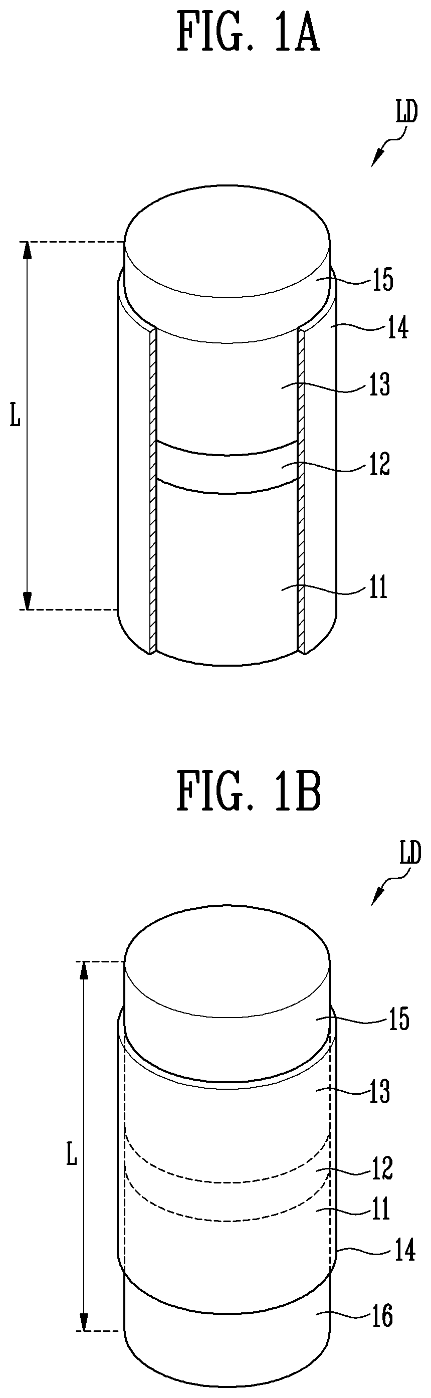
A and 1 B are perspective diagrams schematically illustrating a light emitting element in accordance with an embodiment of the present disclosure.
illustrates a display device in accordance with an embodiment of the present disclosure, and particularly, is a schematic plan view illustrating a display device using the light emitting element illustrated in A as a light emitting source.
A to 3 D are circuit diagrams illustrating examples of a unit light emitting area of the display device of in accordance with various embodiments.
is a plan view schematically illustrating first to third sub-pixels included in one of the pixels illustrated in .
is a sectional view taken along line I-I′ of .
is a schematic plan view illustrating another embodiment of the first sub-pixel in the pixel of .
is a schematic plan view illustrating another embodiment of the first sub-pixel in the pixel of .
A to 8 H are sectional diagrams sequentially illustrating a method of manufacturing the display device of .
illustrates a display device in accordance with an embodiment of the present disclosure, and is a schematic sectional view illustrating a structure of coupling a color conversion layer to the display device of .
schematically illustrates a display device in accordance with an embodiment of the present disclosure, and is a sectional diagram corresponding to line I-I′ of .
A to 11 G are sectional diagrams sequentially illustrating a method of manufacturing the display device of .
illustrates a display device in accordance with an embodiment of the present disclosure, and is a schematic sectional view illustrating a structure of coupling a substrate to the display device of .
MODE FOR INVENTION
As the present disclosure allows for various changes and numerous embodiments, particular embodiments will be illustrated in the drawings and described in detail in the written description. However, this is not intended to limit the present disclosure to particular modes of practice, and it is to be appreciated that all changes, equivalents, and substitutes that do not depart from the spirit and technical scope of the present disclosure are encompassed in the present disclosure.
Throughout the disclosure, like reference numerals refer to like parts throughout the various figures and embodiments of the present disclosure. The sizes of elements in the accompanying drawings may be exaggerated for clarity of illustration. It will be understood that, although the terms “first”, “second”, etc. may be used herein to describe various elements, these elements should not be limited by these terms. These terms are only used to distinguish one element from another element. For instance, a first element discussed below could be termed a second element without departing from the teachings of the present disclosure. Similarly, the second element could also be termed the first element. In the present disclosure, the singular forms are intended to include the plural forms as well, unless the context clearly indicates otherwise.
It will be further understood that the terms “comprise”, “include”, “have”, etc. when used in this specification, specify the presence of stated features, integers, steps, operations, elements, components, and/or combinations of them but do not preclude the presence or addition of one or more other features, integers, steps, operations, elements, components, and/or combinations thereof. Furthermore, when a first part such as a layer, a film, a region, or a plate is disposed on a second part, the first part may be not only directly on the second part but a third part may intervene between them. In addition, when it is expressed that a first part such as a layer, a film, a region, or a plate is formed on a second part, the surface of the second part on which the first part is formed is not limited to an upper surface of the second part but may include other surfaces such as a side surface or a lower surface of the second part. Similarly, when a first part, such as a layer, a film, a region, or a plate is under a second part, the first part may be not only directly under the second part, but a third part may intervene between them.
Embodiments and required details of the present disclosure are described with reference to the accompanying drawings in order to describe the present disclosure in detail so that those having ordinary knowledge in the technical field to which the present disclosure pertains can easily practice the present disclosure. Furthermore, a certain part may be multiple as long as it is not specifically mentioned in a sentence as one or single part.
A and 1 B are perspective diagrams schematically illustrating a light emitting element in accordance with an embodiment of the present disclosure. Although A and 1 B illustrate cylindrical light emitting elements, the present disclosure is not limited thereto.
Referring to A and 1 B , a light emitting element LD in accordance with an embodiment of the present disclosure may include a first conductive semiconductor layer 11 , a second conductive semiconductor layer 13 , and an active layer 12 interposed between the first and second conductive semiconductor layers 11 and 13 . For example, the light emitting element LD may be implemented as a stacked body formed by successively stacking the first conductive semiconductor layer 11 , the active layer 12 , and the second conductive semiconductor layer 13 .
In an embodiment of the present disclosure, the light emitting element LD may be formed in a rod-like shape extending in one direction. If the direction in which the light emitting element LD extends is defined as a longitudinal direction, the light emitting element LD may have a first end and a second end in the extension direction. One of the first and second conductive semiconductor layers 11 and 13 may be disposed on the first end, and the other of the first and second conductive semiconductor layers 11 and 13 may be disposed on the second end.
Although the light emitting element LD may be provided in the form of a cylinder, the present disclosure is not limited thereto. The light emitting element LD may include a rod-like shape or a bar-like shape extending in the longitudinal direction (i.e., to have an aspect ratio greater than 1). For example, a length L of the light emitting element LD with respect to a longitudinal direction may be greater than the diameter thereof. The light emitting element LD may include a light emitting diode fabricated in a subminiature size having a diameter and/or length corresponding to, e.g., a micro-scale or nano-scale size.
However, the size of the light emitting element LD is not limited to this, and the size of the light emitting element LD may be changed to meet the requirements of a lighting device, or a self-emissive display device to which the light emitting element LD is applied.
The first conductive semiconductor layer 11 may include, for example, at least one n-type semiconductor layer. For instance, the first conductive semiconductor layer 11 may include a semiconductor layer which includes any one semiconductor material of InAlGaN, GaN, AlGaN, InGaN, AlN, and InN, and is doped with a first conductive dopant such as Si, Ge, or Sn. The material forming the first conductive semiconductor layer 11 is not limited to this, and the first conductive semiconductor layer 11 may be formed of various other materials.
The active layer 12 may be formed on the first conductive semiconductor layer 11 and have a single or multiple quantum well structure. In an embodiment of the present disclosure, a cladding layer (not illustrated) doped with a conductive dopant may be formed on and/or under the active layer 12 . For example, the cladding layer may be formed of an AlGaN layer or an InAlGaN layer. In addition, material such as AlGaN or AlInGaN may be employed to form the active layer 12 .
If an electric field having a predetermined voltage or more is applied to the opposite ends of the light emitting element LD, the light emitting element LD emits light by coupling of electron-hole pairs in the active layer 12 .
The second conductive semiconductor layer 13 may be provided on the active layer 12 and may include a semiconductor layer of a type different from that of the first conductive semiconductor layer 11 . For example, the second conductive semiconductor layer 13 may include at least one p-type semiconductor layer. For instance, the second conductive semiconductor layer 13 may include a semiconductor layer which includes any one semiconductor material of InAlGaN, GaN, AlGaN, InGaN, AlN, and InN, and is doped with a second conductive dopant such as Mg. The material forming the second conductive semiconductor layer 13 is not limited to this, and the second conductive semiconductor layer 13 may be formed of various other materials.
In an embodiment of the present disclosure, the light emitting element LD may further include one electrode layer 15 disposed on the second conductive semiconductor layer 13 , as illustrated in A , as well as including the first conductive semiconductor layer 11 , the active layer 12 , and the second conductive semiconductor layer 13 . Furthermore, in an embodiment, as shown in B , the light emitting element LD may further include another electrode layer 16 disposed on one end of the first conductive semiconductor layer 11 , as well as including the electrode layer 15 .
Although each of the electrode layers 15 and 16 may be formed of an ohmic contact electrode, the present disclosure is not limited thereto. Furthermore, the electrode layers 15 and 16 may include metal or a metal oxide. For example, chromium (Cr), titanium (Ti), aluminum (Al), gold (Au), nickel (Ni), ITO, and an oxide or alloy thereof may be used alone or in combination with each other. However, the present disclosure is not limited to this.
Materials included in the respective electrode layers 15 and 16 may be equal to or different from each other. The electrode layers 15 and 16 may be substantially transparent or semitransparent. Therefore, light generated from the light emitting element LD may pass through the electrode layers 15 and 16 and then be emitted outside the light emitting element LD.
In an embodiment of the present disclosure, the light emitting element LD may further include an insulating film 14 . However, in some embodiments of the present disclosure, the insulating film 14 may be omitted, or may be provided to cover only some of the first conductive semiconductor layer 11 , the active layer 12 , and the second conductive semiconductor layer 13 .
As illustrated in A , the insulating film 14 may be provided on a portion of the light emitting element LD other than one of opposite ends of the light emitting element LD. In this case, the insulating film 14 may expose only the one electrode layer 15 disposed on one end of the second conductive semiconductor layer 13 of the light emitting element LD and enclose the overall side surfaces of the components other than the electrode layer 15 . Here, the insulating film 14 may allow at least the opposite ends of the light emitting element LD to be exposed to the outside. For example, the insulating film 14 may allow not only the electrode layer 15 disposed on one end of the second conductive semiconductor layer 13 but also one end of the first conductive semiconductor layer 11 to be exposed to the outside.
In an embodiment, as illustrated in B , in the case where the electrode layers 15 and 16 are disposed on the respective opposite ends of the light emitting element LD, the insulating film 14 may allow at least a portion of each of the electrode layers 15 and 16 to be exposed to the outside. Alternatively, in an embodiment, the insulating film 14 may not be provided.
In an embodiment of the present disclosure, the insulating film 14 may include transparent insulating material. For example, the insulating film 14 may include at least one insulating material selected from the group consisting of SiO 2 , Si 3 N 4 , Al 2 O 3 , and TiO 2 , but it is not limited thereto. In other words, various materials having insulating properties may be employed.
If the insulating film 14 is provided on the light emitting element LD, the active layer 12 may be prevented from short-circuiting with a first electrode and/or a second electrode, which is not illustrated. Thanks to the insulating film 14 , occurrence of a defect on the surface of the light emitting element LD may be minimized, whereby the lifetime and efficiency of the light emitting element LD may be improved. In the case where a plurality of light emitting elements LD are disposed in close contact with each other, the insulating film 14 may prevent an undesired short-circuit from occurring between the light emitting elements LD.
The light emitting element LD may be employed as a light source for various display devices. The light emitting element LD may be fabricated through a surface treatment process.
illustrates a display device in accordance with an embodiment of the present disclosure, and particularly, is a schematic plan view illustrating a display device using the light emitting element illustrated in A as a light emitting source.
For the sake of explanation, schematically illustrates the structure of the display device, focused on a display area in which an image is displayed. In some embodiments, although not illustrated, at least one driving circuit (e.g., a scan driver and a data driver) and/or a plurality of lines may be further provided in the display device.
Referring to A and 2 , the display device in accordance with the embodiment of the present disclosure may include a base layer BSL, pixels PXL provided on the base layer BSL and each including at least one light emitting element LD, a driver (not illustrated) provided on the base layer BSL and configured to drive the pixels PXL, and a line component (not illustrated) provided to connect the pixels PXL with the driver.
The display device may be classified into a passive-matrix type display device and an active-matrix type display device according to a driving method. For example, in the case where the display device in accordance with an embodiment is implemented as an active matrix type display device, each of the pixels PXL may include a driving transistor configured to control the amount of current to be supplied to the light emitting element LD, and a switching transistor configured to transmit data signals to the driving transistor.
Recently, active-matrix type display devices capable of selectively turning on each pixel PXL taking into account the resolution, the contrast, and the working speed have been mainstreamed. However, the present disclosure is not limited thereto. For example, passive-matrix type display devices in which pixels PXL may be turned on by groups may also employ components (e.g., first and second electrodes) for driving the light emitting element LD.
The base layer BSL may include a display area DA and a non-display area NDA.
In an embodiment, the display area DA may be disposed in a central portion of the display device, and the non-display area NDA may be disposed in a perimeter portion of the display device in such a way as to enclose the display area DA. The locations of the display area DA and the non-display area NDA are not limited to this, and the locations thereof may be changed.
The display area DA may be an area in which the pixels PXL for displaying an image are provided. The non-display area NDA may be an area in which the driver for driving the pixels PXL and some of the line unit for coupling the pixels PXL to the driver are provided.
The display area DA may have various shapes. For example, the display area DA may be provided in various forms such as a closed polygon including sides formed of linear lines, a circle, an ellipse or the like including a side formed of a curved line, and a semicircle, a semi-ellipse or the like including sides formed of a linear line and a curved line.
The non-display area NDA may be provided on at least one side of the display area DA. In an embodiment of the present disclosure, the non-display area NDA may enclose the display area DA.
The base layer BSL may be a rigid or flexible substrate, and the material or properties thereof are not particularly limited. For example, the base layer BSL may be a rigid substrate made of glass or reinforced glass, or a flexible substrate formed of a thin film made of plastic or metal. Furthermore, the base layer BSL may be a transparent substrate, but it is not limited thereto. For instance, the base layer BSL may be a translucent substrate, an opaque substrate, or a reflective substrate.
The pixels PXL may be disposed in the display area DA on the base layer BSL. Each of the pixels PXL refers to a smallest unit for displaying an image, and a plurality of pixels may be provided.
Each of the pixels PXL may include the light emitting element LD configured to be driven in response to a corresponding scan signal and a corresponding data signal. The light emitting element LD may have a small size corresponding to a nano-scale or a micro-scale, and be connected in parallel to light emitting elements disposed adjacent thereto. The light emitting element LD may form a light source of the corresponding pixel PXL.
Furthermore, each of the pixels PXL may include a plurality of sub-pixels. For example, each pixel PXL may include a first sub-pixel SP 1 , a second sub-pixel SP 2 , and a third sub-pixel SP 3 . In an embodiment, the first, second, and third sub-pixels SP 1 , SP 2 , and SP 3 may emit light of different colors. For instance, the first sub-pixel SP 1 may be a red sub-pixel for emitting red light, the second sub-pixel SP 2 may be a green sub-pixel for emitting green light, and the third sub-pixel SP 3 may be a blue sub-pixel for emitting blue light. However, the colors, types and/or number of sub-pixels forming each pixel PXL are not particularly limited. For example, the color of light which is emitted from each sub-pixel may be changed in various ways. Although in there is illustrated an embodiment where the pixels PXL are arranged in the display area DA in a stripe shape, the present disclosure is not limited thereto. For instance, the display area DA may have various well-known pixel arrangement shapes.
The driver may provide a signal to each pixel PXL through the line component and thus control the operation of the pixel PXL. In , the line component is omitted for the convenience sake of explanation.
The driver may include a scan driver configured to provide scan signals to the pixels PXL through scan lines, an emission driver configured to provide emission control signals to the pixels PXL through emission control lines, a data driver configured to provide data signals to the pixels PXL through data lines, and a timing controller. The timing controller may control the scan driver, the emission driver, and the data driver.
A to 3 D are circuit diagrams illustrating examples of a unit light emitting area of the display device of in accordance with various embodiments.
Referring to A to 3 D , each of the first to third sub-pixels may be configured of an active pixel. However, the type, the configuration, and/or the driving method of each of the first to third sub-pixels is not particularly limited. For example, each of the first to third sub-pixels may be configured of a pixel of a passive or active display device which can have various known structures.
Furthermore, referring to A to 3 D , the first to third sub-pixels may have substantially the same structure or similar structures. Hereinafter, for convenience sake, the first sub-pixel of the first to third sub-pixels will be described as a representative example.
Referring to A, 2 , and 3 A , the first sub-pixel SP 1 may include an emission circuit (or an emission area) EMA configured to generate light having a luminance corresponding to a data signal, and a pixel driving circuit 144 configured to drive the emission circuit EMA.
In an embodiment, the emission circuit EMA may include a plurality of light emitting elements LD connected parallel to each other between a first driving power supply VDD and a second driving power supply VSS (or referred as to second driving power). The first driving power supply VDD and the second driving power supply VSS may have different potentials. For example, the first driving power supply VDD may be set as a high-potential power supply, and the second driving power supply VSS may be set as a low-potential power supply. Here, a difference in potential between the first and second driving power supplies VDD and VSS may be set to a threshold voltage of the light emitting elements LD or more during an emission period of the first sub-pixel SP 1 . A first electrode (e.g., an anode electrode) of each of the light emitting elements LD may be electrically connected to the first driving power supply VDD via the pixel driving circuit 144 . A second electrode (e.g., a cathode electrode) of each of the light emitting elements LD may be electrically connected to the second driving power supply VSS.
Each of the light emitting elements LD may emit light at a luminance corresponding to a driving current which is controlled by the pixel driving circuit 144 .
Although A to 3 C illustrate embodiments in which the light emitting elements LD are connected in parallel to each other in the same direction (e.g., a forward direction) between the first and second driving power supplies VDD and VSS, the present disclosure is not limited thereto. For example, in an embodiment, some of the light emitting elements LD may be connected to each other in the forward direction between the first and second power supplies VDD and VSS, and the other light emitting elements LD may be connected to each other in the reverse direction. One of the first and second driving power supplies VDD and VSS may be supplied in the form of an AC voltage. In this case, the light emitting elements LD connected in the forward direction and the light emitting elements LD connected in the reverse direction may alternately emit light. As another embodiment, in an embodiment, the first sub-pixel SP 1 may include only a single light emitting element LD.
In an embodiment of the present disclosure, the pixel driving circuit 144 may include first and second transistors T 1 and T 2 , and a storage capacitor Cst. The structure of the pixel driving circuit 144 is not limited to that of the embodiment illustrated in A .
A first electrode of the first transistor (switching transistor) T 1 is electrically connected to a data line Dj, and a second electrode thereof is electrically connected to a first node N 1 . Here, the first electrode and the second electrode of the first transistor T 1 may be different electrodes. For example, if the first electrode is a source electrode, the second electrode is a drain electrode. A gate electrode of the first transistor T 1 is connected to the scan line Si.
When a scan signal having a voltage (e.g., a low-level voltage) capable of turning on the first transistor T 1 is supplied from the scan line Si, the first transistor T 1 is turned on to electrically connect the data line Dj with the first node N 1 . Here, a data signal of a corresponding frame is supplied to the data line Dj, whereby the data signal is transmitted to the first node N 1 . The data signal transmitted to the first node N 1 may be charged into the storage capacitor Cst.
A first electrode of the second transistor (driving transistor) T 2 is electrically connected to the first driving power supply VDD, and a second electrode thereof is electrically connected to the first electrode of each of the light emitting elements LD. A gate electrode of the second transistor T 2 is electrically connected to the first node N 1 . As such, the second transistor T 2 may control the amount of driving current to be supplied to the light emitting elements LD in response to the voltage of the first node N 1 .
One electrode of the storage capacitor Cst is electrically connected to the first driving power supply VDD, and the other electrode thereof is electrically connected to the first node N 1 . The storage capacitor Cst is charged with a voltage corresponding to a data signal supplied to the first node N 1 , and maintains the charged voltage until a data signal of a subsequent frame is supplied.
For the sake of explanation, A illustrates the pixel driving circuit 144 having a relatively simple structure including the first transistor T 1 configured to transmit the data signal to the first sub-pixel SP 1 , the storage capacitor Cst configured to store the data signal, and the second transistor T 2 configured to supply driving current corresponding to the data signal to the light emitting elements LD.
However, the present disclosure is not limited thereto, and the structure of the pixel driving circuit 144 may be changed in various ways. For example, the pixel driving circuit 144 may further include at least one transistor element such as a transistor element configured to compensate for the threshold voltage of the second transistor T 2 , a transistor element configured to initialize the first node N 1 , and/or a transistor element configured to control an emission time of the light emitting elements LD, or other circuit elements such as a boosting capacitor for boosting the voltage of the first node N 1 .
Furthermore, although in A the transistors, e.g., the first and second transistors T 1 and T 2 , included in the pixel driving circuit 144 have been illustrated as being formed of P-type transistors, the present disclosure is not limited to this. In other words, at least one of the first and second transistors T 1 and T 2 included in the pixel driving circuit 144 may be changed to an N-type transistor.
Referring to A, 2 , and 3 B , the first and second transistors T 1 and T 2 in accordance with an embodiment of the present disclosure may be formed of N-type transistors. The configuration and operation of the pixel driving circuit 144 illustrated in B , other than a change in connection positions of some components due to a change in the type of transistor, are similar to those of the pixel driving circuit 144 of A . Therefore, detailed descriptions pertaining to this will be omitted.
In an embodiment of the present disclosure, the configuration of the pixel driving circuit 144 is not limited to the embodiments illustrated in A and 3 B . For example, the pixel driving circuit 144 may be configured in the same manner as that of an embodiment illustrated in C .
Referring to A, 2 , and 3 C , the pixel driving circuit 144 may be electrically connected to the scan line Si and the data line Dj of the first sub-pixel SP 1 . For example, if the first sub-pixel SP 1 is disposed on an i-th row and a j-th column of the display area DA, the pixel driving circuit 144 of the first sub-pixel SP 1 may be electrically connected to an i-th scan line Si and a j-th data line Dj of the display area DA.
In an embodiment, the pixel driving circuit 144 may also be electrically connected to at least one scan line. For example, the first sub-pixel SP 1 disposed on the i-th row of the display area DA may be further electrically connected to an i−1-th scan line Si−1 and/or an i+1-th scan line Si+1.
In an embodiment, the pixel driving circuit 144 may be electrically connected not only to the first and second driving power supplies VDD and VSS but also to a third power supply. For example, the pixel driving circuit 144 may also be electrically connected to an initialization power supply Vint.
The pixel driving circuit 144 may include first to seventh transistors T 1 to T 7 , and a storage capacitor Cst.
A first electrode of the first transistor (driving transistor) T 1 , e.g., a source electrode, may be electrically connected to the first driving power supply VDD via the fifth transistor T 5 , and a second electrode thereof, e.g., a drain electrode, may be connected to first end of light emitting elements LD via the sixth transistor T 6 . A gate electrode of the first transistor T 1 may be connected to a first node N 1 . The first transistor T 1 may control driving current flowing between the first driving power supply VDD and the second driving power supply VSS via the light emitting elements LD in response to the voltage of the first node N 1 .
The second transistor (switching transistor) T 2 may be electrically connected between the j-th data line Dj electrically connected to the first sub-pixel SP 1 and the source electrode of the first transistor T 1 . A gate electrode of the second transistor T 2 is electrically connected to the i-th scan line Si electrically connected to the first sub-pixel SP 1 . When a scan signal having a gate-on voltage (e.g., a low-level voltage) is supplied from the i-th scan line Si, the second transistor T 2 is turned on to electrically connect the j-th data line Dj to the source electrode of the first transistor T 1 . Hence, if the second transistor T 2 is turned on, a data signal supplied from the j-th data line Dj may be transmitted to the first transistor T 1 .
The third transistor T 3 is electrically connected between the drain electrode of the first transistor T 1 and the first node N 1 . A gate electrode of the third transistor T 3 is electrically connected to the i-th scan line Si. When a scan signal having a gate-on voltage is supplied from the scan line Si, the third transistor T 3 is turned on to electrically connect the drain electrode of the first transistor T 1 to the first node N 1 . Therefore, when the third transistor T 3 is turned on, the first transistor T 1 may be connected in the form of a diode (or diode-connected).
The fourth transistor T 4 may be electrically connected between the first node N 1 and an initialization power supply Vint. A gate electrode of the fourth transistor T 4 is electrically connected to a preceding scan line, e.g., an i−1-th scan line Si−1. When a scan signal of a gate-on voltage is supplied to the i−1-th scan line Si−1, the fourth transistor T 4 is turned on so that the voltage of the initialization power supply Vint may be transmitted to the first node N 1 . Here, the initialization power supply Vint may have a voltage equal to or less than the minimum voltage of the data signal.
The fifth transistor T 5 is electrically connected between the first driving power supply VDD and the first transistor T 1 . A gate electrode of the fifth transistor T 5 is electrically connected to a corresponding emission control line, e.g., an i-th emission control line Ei. The fifth transistor T 5 may be turned off when an emission control signal having a gate-off voltage is supplied to the i-th emission control line Ei, and may be turned on in other cases.
The sixth transistor T 6 is electrically connected between the first transistor T 1 and first ends of the light emitting elements LD. A gate electrode of the sixth transistor T 6 may be electrically connected to the i-th emission control line Ei. The sixth transistor T 6 may be turned off when an emission control signal having a gate-off voltage is supplied to the i-th emission control line Ei, and may be turned on in other cases.
The seventh transistor T 7 is electrically connected between the first ends of the light emitting elements LD and the initialization power supply Vint. A gate electrode of the seventh transistor T 7 is electrically connected to any one of scan lines of a subsequent stage, e.g., to the i+1-th scan line Si+1. When a scan signal of a gate-on voltage is supplied to the i+1-th scan line Si+1, the seventh transistor T 7 may be turned on so that the voltage of the initialization power supply Vint may be supplied to the first ends of the light emitting elements LD.
The storage capacitor Cst is connected between the first driving power supply VDD and the first node N 1 . The storage capacitor Cst may store a voltage corresponding both to the data signal applied to the first node N 1 during each frame period, and to the threshold voltage of the first transistor T 1 .
For convenience sake, C illustrates that all of the first to seventh transistors T 1 to T 7 are formed of P-type transistors, but the present disclosure is not limited thereto. For example, at least one of the first to seventh transistors T 1 to T 7 included in the pixel driving circuit 144 may be formed of an N-type transistor, or all of the first to seventh transistors T 1 to T 7 may be formed of N-type transistors.
In an embodiment, as illustrated in D , the pixel driving circuit 144 may further include a third transistor T 3 as well as including the first and second transistors T 1 and T 2 . The third transistor T 3 may be connected between the j-th data line Dj and the anode electrode of each of the light emitting elements LD. The gate electrode of the third transistor T 3 may be connected to the control line CLi so that the third transistor T 3 may be turned on when a control signal is supplied to the control line CLi, and be turned off in other cases.
For convenience sake, D illustrates that all of the first to third transistors T 1 to T 3 are formed of P-type transistors, but the present disclosure is not limited thereto. For example, at least one of the first to third transistors T 1 to T 3 included in the pixel driving circuit 144 may be formed of an N-type transistor, or all of the first to third transistors T 1 to T 3 may be formed of N-type transistors.
is a plan view schematically illustrating first to third sub-pixels included in one of the pixels illustrated in , and is a sectional view taken along line I-I′ of .
In , for the sake of explanation, a plurality of light emitting elements provided in each sub-pixel are illustrated as being horizontally aligned. However, the alignment of the light emitting elements is not limited thereto. For example, at least some of the light emitting elements may be aligned in a direction intersecting with the horizontal direction.
Furthermore, for the sake of explanation, illustration of transistors connected to the light emitting elements, and signal lines connected to the transistors has been omitted in .
Moreover, although illustrate a simplified structure of the one pixel, e.g., showing that each electrode has only a single electrode layer, the present disclosure is not limited thereto.
Referring to A to 5 , the display device in accordance with an embodiment of the present disclosure may include a base layer BSL on which a plurality of pixels PXL are provided.
Each of the pixels PXL may include a first sub-pixel SP 1 , a second sub-pixel SP 2 , and a third sub-pixel SP 3 which are provided on the base layer BSL. In an embodiment of the present disclosure, the first sub-pixel SP 1 may be a red sub-pixel, the second sub-pixel SP 2 may be a green sub-pixel, and the third sub-pixel SP 3 may be a blue sub-pixel.
Each of the first to third sub-pixels SP 1 to SP 3 may include an emission area EMA which emits light, and a non-emission PPA disposed around a perimeter of the emission area EMA. In an embodiment of the present disclosure, a pixel area of each of the first to third sub-pixels SP 1 to SP 3 may include an emission area EMA and a non-emission area PPA of the corresponding sub-pixel.
A base layer BSL, a pixel circuit layer PCL, and a display element layer DPL may be provided in the pixel area of each of the first to third sub-pixel SP 1 to SP 3 .
The pixel circuit layer PCL of each of the first to third sub-pixels SP 1 to SP 3 may include a buffer layer BFL disposed on the base layer BSL, first and second transistors T 1 and T 2 disposed on the buffer layer BFL, and a driving voltage line DVL. Furthermore, the pixel circuit layer PCL of each of the first to third sub-pixels SP 1 to SP 3 may further include a passivation layer PSV which is provided on the first and second transistors T 1 and T 2 and the driving voltage line DVL.
The base layer BSL may include insulating material such as glass, an organic polymer, or crystal. Furthermore, the base layer BSL may be made of material having flexibility so as to be bendable or foldable, and have a single-layer or multi-layer structure.
The buffer layer BFL may be provided on the base layer BSL and may prevent impurities from diffusing into the first and second transistors T 1 and T 2 . The buffer layer BFL may be omitted depending on the material of the base layer BSL or processing conditions.
A light shielding pattern SDL may be provided between the base layer BSL and the buffer layer BFL.
The light shielding pattern SDL may be a light shielding layer which is formed of conductive material, insulating material, etc., and blocks light introduced into a rear surface of the base layer BSL so that the light can be blocked from being introduced into the pixel circuit layer PCL of each of the first to third sub-pixels SP 1 , SP 2 , and SP 3 . In an embodiment, the light shielding pattern SDL may include a black matrix. The light shielding pattern SDL may be provided on the base layer BSL to correspond to a lower portion of the semiconductor layer SCL of each of the first and second transistors T 1 and T 2 . In an embodiment, the light shielding pattern SDL may be formed of a metal, which is conductive material. In this case, the light shielding pattern SDL may be electrically connected to a component of any one transistor of the first and second transistors T 1 and T 2 .
The first transistor T 1 may be a driving transistor, which is electrically connected to some of the light emitting elements LD provided in the display element layer DPL of a corresponding sub-pixel to drive the light emitting elements LD. The second transistor T 2 may be a switching transistor configured to switch the first transistor T 1 .
Each of the first and second transistors T 1 and T 2 may include a semiconductor layer SCL, a gate electrode GE, and source and drain electrodes SE and DE.
The semiconductor layer SCL may be disposed on the buffer layer BFL. The semiconductor layer SCL may include a source area which comes into contact with the source electrode SE, and a drain area which comes into contact with the drain electrode DE. An area between the source area and the drain area may be a channel area.
The semiconductor layer SCL may be a semiconductor pattern formed of polysilicon, amorphous silicon, an oxide semiconductor, etc. The channel area may be an intrinsic semiconductor, which is an undoped semiconductor pattern. Each of the source area and the drain area may be a semiconductor pattern doped with an impurity.
The gate electrode GE may be provided on the semiconductor layer SCL with the gate insulating layer GI interposed therebetween.
The source electrode SE and the drain electrode DE may respectively come into contact with the source area and the drain area of the semiconductor layer SCL through corresponding contact holes which pass through an interlayer insulating layer ILD and the gate insulating layer GI.
In an embodiment of the present disclosure, each of the first and second transistors T 1 and T 2 included in the pixel circuit layer PCL provided in each sub-pixel may be formed of an LTPS thin-film transistor, but the present disclosure is not limited thereto. In some embodiments, each of the first and second transistors T 1 and T 2 may be formed of an oxide semiconductor thin-film transistor.
The drain electrode DE of each of the first and second transistors T 1 and T 2 may be electrically connected with the light shielding pattern SDL provided on the base layer BSL. In detail, the drain electrode DE of each of the first and second transistors T 1 and T 2 may be electrically connected to a corresponding light shielding pattern SDL through a contact hole successively passing through the interlayer insulating layer ILD, the gate insulating layer GI, and the buffer layer BFL.
The driving voltage line DVL may be provided on the interlayer insulating layer ILD, but the present disclosure is not limited thereto. In some embodiments, the driving voltage line DVL may be provided on any one of the insulating layers included in the pixel circuit layer PCL. The second driving power supply (VSS of A ) may be applied to the driving voltage line DVL.
The passivation layer PSV may include a first contact hole CH 1 which exposes a portion of the drain electrode DE of the first transistor T 1 , and a second contact hole CH 2 which exposes a portion of the driving voltage line DVL.
The display element layer DPL of each of the first to third sub-pixels SP 1 to SP 3 may include a partition wall PW, first and second electrodes REL 1 and REL 2 , first and second connection lines CNL 1 and CNL 2 , a plurality of light emitting elements LD, and first and second contact electrodes CNE 1 and CNE 2 which are provided on the passivation layer PSV.
The partition wall PW may be provided on the passivation layer PSV in the emission area EMA of each of the first to third sub-pixels SP 1 to SP 3 . A bank BNK formed of the same material as that of the partition wall PW may be formed and/or provided in the non-emission area PPA between adjacent sub-pixels to define the emission area EMA of each sub-pixel.
In an embodiment of the present disclosure, the partition wall PW and the bank BNK may be provided on the same surface and formed and/or provided through the same process. The partition wall PW and the bank BNK may be provided integrally with each other and may include the same material. In the case where the partition wall PW provided in the emission area EMA of each of the first to third sub-pixels SP 1 to SP 3 and the bank BNK provided in the non-emission area PPA of each of the first to third sub-pixels SP 1 to SP 3 are formed and/or provided through the same process, the number of mask processes may be reduced compared to that of the case where the partition wall PW and the bank BNK are separately formed. Detailed description pertaining to this will be made with reference to B .
The partition wall PW may be spaced by a predetermined distance apart from a partition wall PW disposed adjacent thereto on the passivation layer PSV. Two adjacent partition walls PW may be disposed on the passivation layer PSV and spaced apart from each other by a length L of one light emitting element LD or more. Although the partition wall PW may have a trapezoidal cross-section which is reduced in width upward from one surface of the passivation layer PSV, as illustrated in , the present disclosure is not limited thereto.
In an embodiment, the partition wall PW may include a curved surface having a cross-sectional shape such as a semi-circular shape and a semi-elliptical shape, which is reduced in width upward from the one surface of the passivation layer PSV. In a sectional view, the shape of each of the partition walls PW is not limited to the foregoing examples, and may be changed in various ways within a range in which the efficiency of light emitted from each of the light emitting elements LD can be enhanced. The two adjacent partition walls PW may be disposed on the same plane on the passivation layer PSV and have the same height.
The first connection line CNL 1 may extend from each of the first to third sub-pixels SP 1 to SP 3 in a first direction DR 1 . The first connection line CNL 1 may be provided in only one corresponding sub-pixel so as to independently drive each of the first to third sub-pixels SP 1 to SP 3 .
The second connection line CNL 2 may extend in a direction parallel to a direction in which the first connection line CNL 1 extends. The second connection line CNL 2 may be provided in common to the first to third sub-pixels SP 1 to SP 3 . Therefore, the first to third sub-pixels SP 1 to SP 3 may be connected in common to the second connection line CNL 2 .
Each of the first and second electrodes REL 1 and REL 2 may be provided in the emission area EMA of each of the first to third sub-pixels SP 1 to SP 3 and extend in a second direction DR 2 intersecting with the first direction DR 1 . The first and second electrodes REL 1 and REL 2 may be provided on the same plane and spaced apart from each other by a predetermined distance.
The first electrode REL 1 may be connected to the first connection line CNL 1 . For instance, the first electrode REL 1 may be integrally connected to the first connection line CNL 1 . For instance, the first electrode REL 1 may include a 1-1-th electrode REL 1 _ 1 and a 1-2-th electrode REL 1 _ 2 which diverge in the second direction DR 2 from the first connection line CNL 1 extending in the first direction DR 1 . The 1-1-th electrode REL 1 _ 1 , the 1-2-th electrode REL 1 _ 2 , and the first connection line CNL 1 may be integrally provided and electrically and/or physically connected to each other. In the case where the first electrode REL 1 and the first connection line CNL 1 are formed and/or provided integrally with each other, the first connection line CNL 1 may be regarded as one area of the first electrode RELl. However, the present disclosure is not limited thereto. For example, in some embodiments, the first electrode REL 1 and the first connection line CNL 1 may be individually formed and electrically connected to each other through a contact hole, via hole, or the like, which is not illustrated.
The second electrode REL 2 may extend in the second direction DR 2 and be electrically connected with the second connection line CNL 2 . In an embodiment of the present disclosure, the second electrode REL 2 may diverge from the second connection line CNL 2 in the second direction DR 2 . Hence, the second electrode REL 2 and the second connection line CNL 2 may be integrally provided and electrically and/or physically connected to each other. In the case where the second electrode REL 2 and the second connection line CNL 2 are formed and/or provided integrally with each other, the second connection line CNL 2 may be regarded as one area of the second electrode REL 2 . However, the present disclosure is not limited thereto. For example, in some embodiments, the second electrode REL 2 and the second connection line CNL 2 may be individually formed and electrically connected to each other through a contact hole, via hole, or the like, which is not illustrated.
Each of the first and second electrodes REL 1 and REL 2 may function as an alignment electrode for aligning the light emitting elements LD in the emission area EMA of each of the first to third sub-pixels SP 1 to SP 3 .
Before the light emitting elements LD are aligned in the emission area EMA of each of the first to third sub-pixels SP 1 to SP 3 , a first alignment voltage may be applied to the first electrode REL 1 through the first connection line CNL 1 , and a second alignment voltage may be applied to the second electrode REL 2 through the second connection line CNL 2 . The first alignment voltage and the second alignment voltage may have different voltage levels. As predetermined alignment voltages having different voltage levels are respectively applied to the first electrode REL 1 and the second electrode REL 2 , an electric field may be formed between the first electrode REL 1 and the second electrode REL 2 . Hence, the light emitting elements LD may be aligned between the first electrode REL 1 and the second electrode REL 2 .
In a plan view, the second electrode REL 2 may be provided between the 1-1-th electrode REL 1 _ 1 and the 1-2-th electrode REL 1 _ 2 and spaced apart from each of the 1-1-th and 1-2-th electrodes REL 1 _ 1 and REL 1 _ 2 by a predetermined distance. The 1-1-th electrode REL 1 _ 1 , the 1-2-th electrode REL 1 _ 2 , and the second electrode REL 2 may be alternately disposed on the passivation layer PSV.
After the light emitting elements LD are aligned in the emission area EMA of each of the first to third sub-pixels SP 1 to SP 3 , each of the first and second electrodes REL 1 and REL 2 may function as a driving electrode for driving the light emitting elements LD.
The first and second electrodes REL 1 and REL 2 may be made of material having a predetermined reflectivity to allow light emitted from the opposite ends EP 1 and EP 2 of each of the light emitting elements LD to travel in a direction (e.g., in a frontal direction) in which an image of the display device is displayed.
In an embodiment of the present disclosure, the first and second electrodes REL 1 and REL 2 , the first connection line CNL 1 , and the second connection line CNL 2 may be provided on the same layer and formed of the same material.
The first and second electrodes REL 1 and REL 2 , the first connection line CNL 1 , and the second connection line CNL 2 may be formed of conductive material having a predetermined reflectivity. The conductive material may include metal such as Ag, Mg, Al, Pt, Pd, Au, Ni, Nd, Ir, Cr, or an alloy of them, a conductive oxide such as an indium tin oxide (ITO), an indium zinc oxide (IZO), a zinc oxide (ZnO), or an indium tin zinc oxide (ITZO), and a conductive polymer such as PEDOT.
The materials of the first and second electrodes REL 1 and REL 2 , the first connection line CNL 1 , and the second connection line CNL 2 are not limited to the foregoing materials.
Each of the first and second electrodes REL 1 and REL 2 , the first connection line CNL 1 , and the second connection line CNL 2 may have a single layer structure, but the present disclosure is not limited thereto, for example, it may have a multi-layer structure formed by stacking two or more materials of metals, alloys, conductive oxides, and conductive polymers.
Each of the first and second electrodes REL 1 and REL 2 , the first connection line CNL 1 , and the second connection line CNL 2 may have a multi-layer structure having at least two or more layers to minimize a voltage drop due to a signal delay when signals are transmitted to the opposite ends EP 1 and EP 2 of each of the light emitting elements LD.
Since the first and second electrodes REL 1 and REL 2 have shapes corresponding to the shape of the partition wall PW, light emitted from the opposite ends EP 1 and EP 2 of each of the light emitting elements LD may be reflected by the first and second electrodes REL 1 and REL 2 and more effectively travel in the frontal direction of the display device. Consequently, the efficiency of light emitted from the light emitting elements LD may be enhanced.
In an embodiment of the present disclosure, the partition wall PW and the first and second electrodes REL 1 and REL 2 may function as reflective components enabling light emitted from each of the light emitting elements LD to travel in the frontal direction of the display device, thus enhancing the light output efficiency of the light emitting elements LD.
Any one of the first and second electrodes REL 1 and REL 2 may be an anode electrode, and the other may be a cathode electrode. In an embodiment of the present disclosure, the first electrode REL 1 may be an anode electrode, and the second electrode REL 2 may be a cathode electrode.
Each of the light emitting elements LD may be formed of a light emitting diode which is made of material having an inorganic crystal structure and has a subminiature size, e.g., corresponding to a nano-scale or micro-scale size.
Although at least two or tens of light emitting elements LD are provided in the emission area EMA of each of the first to third sub-pixels SP 1 , SP 2 , and SP 3 , the present disclosure is not limited thereto. In an embodiment, the number of light emitting elements LD provided in each sub-pixel may be changed in various ways.
Each of the light emitting elements LD may include a stacked emission pattern formed by successively stacking a first conductive semiconductor layer 11 , an active layer 12 , a second conductive semiconductor layer 13 , and an electrode layer 15 in the longitudinal direction (L) of each light emitting element LD. Furthermore, each of the light emitting elements LD may further include an insulating film 14 which encloses an outer circumferential surface of the stacked emission pattern. In an embodiment of the present disclosure, each of the light emitting elements LD may have a cylindrical shape. In this case, each light emitting element LD may have a first end EP 1 corresponding to any one of a lower portion of the cylinder and an upper portion of the cylinder, and a second end EP 2 corresponding to the other of the lower portion of the cylinder and the upper portion of the cylinder. Any one of the first conductive semiconductor layer 11 and the electrode layer 15 may be disposed on the first end EP 1 of each light emitting element LD, and the other of the first conductive semiconductor layer 11 and the electrode layer 15 may be disposed on the second end EP 2 thereof.
In an embodiment of the present disclosure, the light emitting elements LD may be divided into a plurality of first light emitting elements LD 1 aligned between the 1-1-th electrode REL 1 _ 1 and the second electrode REL 2 , and a plurality of second light emitting elements LD 2 aligned between the second electrode REL 2 and the 1-2-th electrode REL 1 _ 2 .
A second insulating layer INS 2 for covering a portion of an upper surface of each of the light emitting elements LD may be provided on the light emitting elements LD. A first insulating layer INS 1 may be provided between each of the light emitting elements LD and the passivation layer PSV.
The first insulating layer INS 1 may be filled into space between the passivation layer PSV and each of the light emitting elements LD to stably support the light emitting elements LD and prevent the light emitting elements LD from being removed from the passivation layer PSV. The first insulating layer INS 1 may be formed of an inorganic insulating layer including inorganic material, or an organic insulating layer including organic material. Although in an embodiment of the present disclosure the first insulating layer INS 1 may be formed of an inorganic insulating layer having an advantage in protecting the light emitting elements LD from the pixel circuit layer PCL, the present disclosure is not limited thereto. In an embodiment, the first insulating layer INS 1 may be formed of an organic insulating layer that has an advantage in planarization of support surfaces of the light emitting elements LD.
The second insulating layer INS 2 may be an organic insulating layer including organic material. In an embodiment of the present disclosure, the second insulating layer INS 2 may be provided on a portion of the upper surface of each of the light emitting elements LD such that the opposite ends EP 1 and EP 2 of each of the light emitting elements LD may be exposed to the outside.
In an embodiment of the present disclosure, the first connection line CNL 1 may be electrically connected to the drain electrode DE of the first transistor T 1 through the first contact hole CH 1 of the passivation layer PSV. Since the first connection line CNL 1 is integrally provided with the first electrode REL 1 , a signal of the first transistor T 1 applied to the first connection line CNL 1 may be transmitted to the first electrode REL 1 .
The first electrode REL 1 may be disposed adjacent to one end of the opposite ends EP 1 and EP 2 of each of the light emitting elements LD, and may be electrically connected to each of the light emitting elements LD through the first contact electrode CNE 1 . Therefore, a signal of the first transistor T 1 that is applied to the first electrode REL 1 may be transmitted to each of the light emitting elements LD through the first contact electrode CNE 1 .
In an embodiment of the present disclosure, the second connection line CNL 2 may be electrically connected to the driving voltage line DVL through the second contact hole CH 2 of the passivation layer PSV. Since the second connection line CNL 2 is integrally provided with the second electrode REL 2 , the voltage of the second driving power supply VSS of the driving voltage line DVL applied to the second connection line CNL 2 may be transmitted to the second electrode REL 2 .
The second electrode REL 2 may be disposed adjacent to the other end of the opposite ends EP 1 and EP 2 of each of the light emitting elements LD, and may be electrically connected to each of the light emitting elements LD through the second contact electrode CNE 2 . Hence, the voltage of the second driving power VSS applied to the second electrode REL 2 may be transmitted to each of the light emitting elements LD.
The first contact electrode CNE 1 may be provided on the first electrode REL 1 to electrically and/or physically reliably connect the first electrode REL 1 with one end of the opposite ends EP 1 and EP 2 of each of the light emitting elements LD. The first contact electrode CNE 1 may be formed of transparent conductive material to allow light emitted from each of the light emitting elements LD and reflected by the first electrode REL 1 in the frontal direction of the display device to travel in the frontal direction without loss.
In a plan view, the first contact electrode CNE 1 may cover the first electrode REL 1 and overlap with the first electrode RELl. Furthermore, the first contact electrode CNE 1 may partially overlap with one of the opposite ends EP 1 and EP 2 of each of the light emitting elements LD. The first contact electrode CNE 1 may include a 1-1-th contact electrode CNE 1 _ 1 provided on the 1-1-th electrode REL 1 _ 1 , and a 1-2-th contact electrode CNE 1 _ 2 provided on the 1-2-th electrode REL 1 _ 2 .
The second contact electrode CNE 2 may be provided on the second electrode REL 2 . In a plan view, the second contact electrode CNE 2 may cover the second electrode REL 2 and overlap with the second electrode REL 2 . Furthermore, the second contact electrode CNE 2 may overlap with the second end EP 2 of each of the first light emitting elements LD 1 and the first end EP 1 of each of the second light emitting elements LD 2 . The second contact electrode CNE 2 may be made of the same material as that of the first contact electrode CNE 1 , but the present disclosure is not limited thereto.
In an embodiment of the present disclosure, the first contact electrode CNE 1 and the second contact electrode CNE 2 may be provided on the same plane and spaced apart from each other by a predetermined distance on the second insulating layer INS 2 so that the first and second contact electrodes CNE 1 and CNE 2 can be electrically and/or physically separated from each other. In other words, the first contact electrode CNE 1 and the second contact electrode CNE 2 may be provided on the same layer and formed through the same manufacturing process.
A third insulating layer INS 3 for covering the first and second contact electrodes CNE 1 and CNE 2 may be provided on the first contact electrode CNE 1 and the second contact electrode CNE 2 . The third insulating layer INS 3 may prevent the first and second contact electrodes CNE 1 and CNE 2 from being exposed to the outside, thus preventing the first and second contact electrodes CNE 1 and CNE 2 from being corroded.
The third insulating layer INS 3 may be formed of an inorganic insulating layer including inorganic material, or an organic insulating layer including organic material. Although the third insulating layer INS 3 may have a single layer structure as shown in the drawing, the present disclosure is not limited thereto. For example, the third insulating layer INS 3 may have a multi-layer structure. In the case where the third insulating layer INS 3 has a multi-layer structure, the third insulating layer INS 3 may have a structure formed by alternately stacking a plurality of inorganic insulating layers and a plurality of organic insulating layers. For example, the third insulating layer INS 3 may have a structure formed by sequentially stacking a first inorganic insulating layer, an organic insulating layer, and a second inorganic insulating layer.
An overcoat layer (not illustrated) may be provided over the third insulating layer INS 3 . The overcoat layer may be a planarization layer for mitigating a step difference formed by the partition wall PW, the first and second electrodes REL 1 and REL 2 , the first and second contact electrodes CNE 1 and CNE 2 , etc. that are disposed under the overcoat layer. The overcoat layer may be an encapsulating layer provided to prevent oxygen, water, or the like from penetrating into the light emitting elements LD.
Predetermined voltages may be respectively applied to the opposite ends EP 1 and EP 2 of each of the light emitting elements LD through the first electrode REL 1 and the second electrode REL 2 . Hence, each of the light emitting elements LD may emit light by coupling of electron-hole pairs in the active layer 12 of each of the light emitting elements LD. Here, the active layer 12 may emit light having a wavelength range from 400 nm to 900 nm.
is a schematic plan view illustrating another embodiment of the first sub-pixel in the pixel of .
The configuration of the first sub-pixel illustrated in , other than a structure in which an emission area includes first and second sub-emission areas and alignment shapes of electrodes are different from each other in respective sub-emission areas, may be substantially equal or similar to that of the first sub-pixel of .
Therefore, to avoid redundant explanation, the description of the first sub-pixel of will be focused on differences from that of the foregoing embodiments. Components which are not separately explained in the following description of the present embodiment comply with that of the foregoing embodiments. The same reference numeral will be used to designate the same component, and a similar reference numeral will be used to designate a similar component.
Referring to A, 2 , 4 , and 6 , the first sub-pixel SP 1 may include an emission area EMA which may emit light, and a non-emission area PPA disposed around the emission area EMA.
A display element layer (refer to DPL of ) of the first sub-pixel SP 1 may include a partition wall PW, first and second electrodes REL 1 and REL 2 , first and second connection lines CNL 1 and CNL 2 , a plurality of light emitting elements LD, and first and second contact electrodes CNE 1 and CNE 2 which are provided on a circuit element layer (refer to PCL of ).
The light emitting elements LD may include first light emitting elements LD 1 and the second light emitting elements LD 2 . The first light emitting elements LD 1 each may include first and second ends EP 1 and EP 2 with respect to a first direction DR 1 . Here, the first direction DR 1 may refer to a horizontal direction in a plan view. The second light emitting elements LD 2 each may include first and second ends EP 1 and EP 2 with respect to a second direction DR 2 intersecting with the first direction DR 1 . Here, the second direction DR 2 may refer to a vertical direction in a plan view. The first light emitting elements LD 1 may be aligned in the horizontal direction, and the second light emitting elements LD 2 may be aligned in the vertical direction.
In an embodiment of the present disclosure, the emission area EMA of the first sub-pixel SP 1 may include a first sub-emission area SEMA 1 in which the first light emitting elements LD 1 are provided, and a second sub-emission area SEMA 2 in which the second light emitting elements LD 2 are provided.
In an embodiment of the present disclosure, the first electrode REL 1 may include a 1-1-th electrode REL 1 _ 1 and a 1-2-th electrode REL 1 _ 2 , and the second electrode REL 2 may include a 2-1-th electrode REL 2 _ 1 and a 2-2-th electrode REL 2 _ 2 .
In a plan view, a portion of the first electrode REL 1 and a portion of the second electrode REL 2 may be alternately provided in the first direction DR 1 in the first sub-emission area SEMA 1 . For example, the 1-1-th electrode REL 1 _ 1 of the first electrode REL 1 and the 2-1-th electrode REL 2 _ 1 of the second electrode REL 2 may be alternately provided in the first direction DR 1 in the first sub-emission area SEMA 1 .
In a plan view, the other portion of the first electrode REL 1 and the other portion of the second electrode REL 2 may be alternately provided in the second direction DR 2 in the second sub-emission area SEMA 2 . For example, the 1-2-th electrode REL 1 _ 2 of the first electrode REL 1 and the 2-2-th electrode REL 2 _ 2 of the second electrode REL 2 may be alternately provided in the second direction DR 2 in the second sub-emission area SEMA 2 .
In an embodiment of the present disclosure, the first contact electrode CNE 1 may include a 1-1-th contact electrode CNE 1 _ 1 which is provided on the 1-1-th electrode REL 1 _ 1 and overlaps with the 1-1-th electrode REL 1 _ 1 in a plan view, and a 1-2-th contact electrode CNE 1 _ 2 which is provided on the 1-2-th electrode REL 1 _ 2 and overlaps with the 1-2-th electrode REL 1 _ 2 in a plan view.
Furthermore, the second contact electrode CNE 2 may include a 2-1-th contact electrode CNE 2 _ 1 which is provided on the 2-1-th electrode REL 2 _ 1 and overlaps with the 2-1-th electrode REL 2 _ 1 in a plan view, and a 2-2-th contact electrode CNE 2 _ 2 which is provided on the 2-2-th electrode REL 2 _ 2 and overlaps with the 2-2-th electrode REL 2 _ 2 in a plan view.
A distance between the 1-1-th and 2-1-th electrodes REL 1 _ 1 and REL 2 _ 1 in the first sub-emission area SEMA 1 and a distance between the 1-2-th and 2-2-th electrodes REL 1 _ 2 and REL 2 _ 2 in the second sub-emission area SEMA 2 , may be designed to be the same as each other. The reason for this is because an alignment surface area of the first light emitting elements LD 1 aligned in the first sub-emission area SEMA 1 can be formed to be the same as an alignment surface area of the second light emitting elements LD 2 aligned in the second sub-emission area SEMA 2 . In the case where the respective alignment surface areas of the first and second sub-emission areas SEMA 1 and SEMA 2 are the same as each other, the first and second light emitting elements LD 1 and LD 2 may be prevented from being biased to one area.
A bank BNK disposed on the same plane as that of the partition wall PW may be provided in the non-emission area PPA of the first sub-pixel SP 1 . The bank BNK may be formed and/or provided in the non-emission area PPA between the first sub-pixel SP 1 and sub-pixels adjacent to the first sub-pixel SP 1 to define the emission area EMA of each sub-pixel.
In an embodiment of the present disclosure, the partition wall PW and the bank BNK may be formed of an organic insulating material including organic material, but the present disclosure is not limited thereto. In an embodiment, the partition wall PW and the bank BNK may be formed of an inorganic insulating material including inorganic material, or conductive material which may be prevented from directly affecting the first and second electrodes REL 1 and REL 2 and the light emitting elements LD due to reflection of external light.
In an embodiment of the present disclosure, for the sake of explanation, there is illustrated an example where the bank BNK provided in the non-emission area PPA of the first sub-pixel SP 1 is provided integrally with the partition wall PW provided in each of the first and second sub-emission areas SEMA 1 and SEMA 2 and thus physically connected with the partition wall PW. However, the present disclosure is not limited to this. In an embodiment, the bank BNK may be provided in the non-emission area PPA of the first sub-pixel SP 1 , such that the bank BNK is spaced apart from the partition wall PW by a predetermined distance on the same plane.
In the non-emission area PPA of the first sub-pixel SP 1 , the first and second connection lines CNL 1 and CNL 2 may be provided on a corresponding bank BNK, and thus overlap with the corresponding bank BNK in a plan view.
is a schematic plan view illustrating another embodiment of the first sub-pixel in the pixel of .
To avoid redundant explanation, the description of the first sub-pixel of will be focused on differences from that of the foregoing embodiments. Components which are not separately explained in the following description of the present embodiment comply with that of the foregoing embodiments. The same reference numeral will be used to designate the same component, and a similar reference numeral will be used to designate a similar component.
For the convenience sake of illustration, illustrates only first and second electrodes, light emitting elements provided between the first and second electrodes, and a second connection line connected to the second electrode.
Referring to A, 2 , 4 , and 7 , the first sub-pixel SP 1 may include an emission area EMA which may emit light, and a non-emission area PPA disposed around the emission area EMA.
A display element layer (refer to DPL of ) of the first sub-pixel SP 1 may include first and second electrodes REL 1 and REL 2 , a second connection line CNL 2 , and a plurality of light emitting elements LD which are provided on a circuit element layer (refer to PCL of ).
In an embodiment of the present disclosure, the first and second electrodes REL 1 and REL 2 may be provided on the same plane on the passivation layer PSV and be electrically connected with the light emitting elements LD. Each of the first and second electrodes REL 1 and REL 2 may have a circular shape. In this case, if the first and second electrodes REL 1 and REL 2 are respectively supplied with corresponding alignment voltages, an electric field having a radial shape may be formed between the first and second electrodes REL 1 and REL 2 . Hence, the light emitting elements LD may be aligned in various directions along the circumference of the first electrode REL 1 .
As illustrated in A , each of the light emitting elements LD may have a cylindrical shape. Particularly, each of the light emitting elements LD may include first and second ends EP 1 and EP 2 in the longitudinal direction (L). The first conductive semiconductor layer 11 may be disposed on any one of the first and second ends EP 1 and EP 2 of each of the light emitting elements LD. The electrode layer 15 may be disposed on the other of the first and second ends EP 1 and EP 2 of each of the light emitting elements LD.
Although as shown in the drawings, each of the first and second electrodes REL 1 and REL 2 may have a circular shape, the present disclosure is not limited thereto, and it may have various shapes such as an elliptical shape, a rectangular shape, and a polygonal shape.
The first electrode REL 1 and the second electrode REL 2 may be provided in the emission area EMA of the first sub-pixel SP 1 . The second electrode REL 2 may be provided in a shape enclosing the perimeter of the first electrode REL 1 . Particularly, the second electrode REL 2 may extend in a circumferential direction around the first electrode REL 1 . In an embodiment of the present disclosure, the second electrode REL 2 may include a 2-1-th electrode REL 2 - 1 and a 2-2-th electrode REL 2 _ 2 . The 2-1-th electrode REL 2 _ 1 and the 2-2-th electrode REL 2 _ 2 may be spaced apart from each other by a predetermined distance.
The 2-1-th electrode REL 2 _ 1 may be electrically connected to another 2-1-th electrode REL 2 _ 1 disposed on the same column in the second direction DR 2 through the 2-1-th connection line CNL 2 _ 1 . The 2-2-th electrode REL 2 _ 2 may be electrically connected to another 2-2-th electrode REL 2 _ 2 disposed on the same column in the second direction DR 2 through the 2-2-th connection line CNL 2 _ 2 .
A to 8 H are sectional diagrams sequentially illustrating a method of manufacturing the display device of .
Referring to A to 8 A , the pixel circuit layer PCL is formed on the respective base layers BSL of the first to third sub-pixels SP 1 , SP 2 , and SP 3 . The pixel circuit layer PCL may include the light shielding pattern SDL, the first and second transistors T 1 and T 2 , the driving voltage line DVL, and the passivation layer PSV.
The passivation layer PSV may include the first contact hole CH 1 which exposes the drain electrode DE of the first transistor T 1 , and the second contact hole CH 2 which exposes the driving voltage line DVL.
Referring to A to 8 B , after an insulating material layer (not illustrated) is applied to the passivation layer PSV, the partition wall PW is formed in the emission area EMA of each of the first to third sub-pixels SP 1 , SP 2 , and SP 3 by patterning the insulating material layer using a mask (not illustrated), and simultaneously, the bank BNK is formed in the non-emission area PPA between the first to third sub-pixels SP 1 , SP 2 , and SP 3 . The mask that is used during the above-mentioned manufacturing process may be a half-tone mask.
In an embodiment of the present disclosure, the partition wall PW and the bank BNK may be provided on the same surface and may include the same material. For example, the partition wall PW and the bank BNK each may be an organic insulating layer including organic material.
As described above, in the case where the passivation layer PSV and the partition wall PW are formed through the same process, the number of masks may be reduced compared to that of the case where the passivation layer PSV and the partition wall PW are formed through separate processes. Hence, the process of manufacturing the display device may be further simplified.
Referring to A to 8 C , the first and second electrodes REL 1 and REL 2 and the first and second connection lines CNL 1 and CNL 2 that include conductive material having a high reflectivity are formed on the passivation layer PSV of each sub-pixel including the partition wall PW.
Each of the first and second electrodes REL 1 and REL 2 may be provided and/or formed on a corresponding partition wall PW in the emission area EMA of each sub-pixel. Each of the first and second connection lines CNL 1 and CNL 2 may be provided and/or formed in the non-emission area PPA of each sub-pixel.
In an embodiment of the present disclosure, the first connection line CNL 1 may be electrically connected to the first transistor T 1 of the pixel circuit layer PCL through the first contact hole CH 1 of the passivation layer PSV. The first connection line CNL 1 may be provided integrally with the first electrode REL 1 and electrically and/or physically connected to the first electrode REL 1 . Hence, a signal (or a voltage) applied to the first transistor T 1 may be transmitted to the first electrode REL 1 through the first connection line CNL 1 .
The second connection line CNL 2 may be electrically connected to the driving voltage line DVL of the pixel circuit layer PCL through the second contact hole CH 2 of the passivation layer PSV. The second connection line CNL 2 may be provided integrally with the second electrode REL 2 and electrically and/or physically connected to the second electrode REL 2 . Consequently, the voltage of the second driving power VSS of the driving voltage line DVL may be transmitted to the second electrode REL 2 through the second connection line CNL 2 .
Referring to A to 8 D , after an insulating material layer (not illustrated) is deposited on the passivation layer PSV on which the first and second electrodes REL 1 and REL 2 are formed, the first insulating layer INS 1 is formed by patterning the insulating material layer using a mask (not illustrated).
The first insulating layer INS 1 may be formed and/or provided in the emission area EMA of each sub-pixel between the first electrode REL 1 and the second electrode REL 2 and may be formed and/or provided on the first and second connection lines CNL 1 and CNL 2 in the non-emission area PPA of each sub-pixel.
Referring to A to 8 E , an electric field is formed between the first electrode REL 1 and the second electrode REL 2 by respectively applying corresponding alignment voltages to the first and second electrodes REL 1 and REL 2 of each sub-pixel through the first and second connection lines CNL 1 and CNL 2 . In the case where direct current power or alternating current power having predetermined voltage and period is repeatedly applied several times to each of the first and second electrodes REL 1 and REL 2 through the first and second connection lines CNL 1 and CNL 2 , an electric field may be formed between the first and second electrodes REL 1 and REL 2 by a difference in potential between the first and second electrodes REL 1 and REL 2 .
After an electric field is formed between the first electrode REL 1 and the second electrode REL 2 that are formed in the emission area EMA of each sub-pixel, light emitting elements LD are supplied in an inkjet printing scheme or the like. For example, the light emitting elements LD may be supplied onto the passivation layer PSV of the emission area EMA of such sub-pixel by disposing a nozzle over the passivation layer PSV and dropping a solution including the light emitting elements LD onto the passivation layer PSV through the nozzle. The solution may be any one of acetone, water, alcohol, and toluene, but the present disclosure is not limited thereto. For example, the solution may include material which may be vaporized at the room temperature or by heat. Furthermore, the solution may have the form of ink or paste. A method of supplying the light emitting elements LD is not limited to the foregoing method. The method of supplying the light emitting elements LD may be changed. Subsequently, the solution may be removed.
If the light emitting elements LD are supplied onto the passivation layer PSV, self-alignment of the light emitting elements LD may be induced by the electric field formed between the first electrode REL 1 and the second electrode REL 2 . Hence, the light emitting elements LD may be aligned between the first electrode REL 1 and the second electrode REL 2 . In other words, the light emitting elements LD may be intensively aligned in a target area, e.g., the emission area EMA of each sub-pixel.
Referring to A to 8 F , after the alignment of the light emitting elements LD, the second insulating layer INS 2 that covers a portion of the upper surface of each light emitting element LD is formed by applying an insulating material layer (not illustrated) onto the passivation layer PSV and patterning the insulating material layer using a mask (not illustrated). Hence, the opposite ends EP 1 and EP 2 of each of the light emitting elements LD may be exposed to the outside.
Referring to A to 8 G , after a conductive layer (not illustrated) is formed on the second insulating layer INS 2 over an entire surface of the passivation layer PSV, the first and second contact electrodes CNE 1 and CNE 2 are formed by patterning the conductive layer using a mask (not illustrated).
The first contact electrode CNE 1 and the second contact electrode CNE 2 may be spaced apart from each other by a predetermined distance on the second insulating layer INS 2 and thus electrically and/or physically separated from each other.
A portion of the first connection line CNL 1 connected and/or provided in common to the sub-pixels may be removed through the foregoing mask process so that each sub-pixel can be driven independently from adjacent sub-pixels. Hence, each sub-pixel may be individually driven, and the display device in accordance with an embodiment of the present disclosure may be implemented as an active matrix-type display device.
Referring to A to 8 H , the third insulating layer INS 3 is formed on the first and second contact electrodes CNE 1 and CNE 2 .
In the display device manufactured through the foregoing manufacturing process, during a process of manufacturing the display element layer DPL, the partition wall PW is formed in the emission area EMA of each sub-pixel, and simultaneously, the bank BNK is formed in the non-emission area PPA of each sub-pixel. Hence, the number of mask processes may be reduced.
illustrates a display device in accordance with an embodiment of the present disclosure, and is a schematic sectional view illustrating a structure of coupling a color conversion layer to the display device of .
schematically illustrates a pixel area of one pixel of a plurality of pixels included in the display device, for the convenience sake of explanation.
Furthermore, for the convenience sake, in , structures of some components equal to those of the display device that are described in detail with reference to are schematically illustrated, and detailed explanation thereof will be omitted.
Referring to A to 9 , the display device in accordance with an embodiment of the present disclosure may include a display panel DP that includes a first substrate SUB 1 on which at least one pixel PXL (hereinafter, referred to as ‘pixel’) including first to third sub-pixels SP 1 , SP 2 , and SP 3 is provided, and a second substrate SUB 2 connected with the first substrate SUB 1 .
In an embodiment of the present disclosure, the pixel PXL is formed and/or provided in the pixel area PXA defined on the first substrate SUB 1 . The pixel area PXA may include a first sub-pixel area SPAT in which a first sub-pixel SP 1 is formed and/or provided, a second sub-pixel area SPA 2 in which a second sub-pixel SP 2 is formed and/or provided, and a third sub-pixel area SPA 3 in which a third sub-pixel SP 3 is formed and/or provided.
In an embodiment of the present disclosure, the first substrate SUB 1 may include a base layer BSL, and a pixel circuit layer PCL provided on the base layer BSL. The display element layer DPL may be provided on the first substrate SUB 1 .
The display element layer DPL may include a partition wall PW, first and second electrodes REL 1 and REL 2 , a plurality of light emitting elements LD, and first and second contact electrodes CNE 1 and CNE 2 which are provided on the pixel circuit layer PCL of the emission area EMA of each of the first to third sub-pixels SP 1 , SP 2 , and SP 3 . Furthermore, the display element layer DPL may include a bank BNK provided in the non-emission area PPA of each of the first to third sub-pixels SP 1 , SP 2 , and SP 3 .
In an embodiment of the present disclosure, the partition wall PW and the bank BNK may be provided on the same surface and formed through the same process. In an embodiment of the present disclosure, the first and second contact electrodes CNE 1 and CNE 2 may be provided on the same surface and formed through the same process.
Each of the light emitting elements LD may include opposite ends EP 1 and EP 2 with respect to the longitudinal direction (L).
The second substrate SUB 2 may be disposed over the first substrate SUB 1 to cover the display area DA on which the first to third sub-pixels SP 1 , SP 2 , and SP 3 are disposed. The second substrate SUB 2 may form an upper substrate (e.g., an encapsulation substrate or a thin-film encapsulation layer) and/or a window component of the display panel DP. In an embodiment, the second substrate SUB 2 may be a rigid substrate or a flexible substrate, and the material or properties thereof are not particularly limited. Furthermore, the second substrate SUB 2 may be formed of the same material as that of the first substrate SUB 1 , or may be formed of material different from that of the first substrate SUB 1 .
Furthermore, the display panel DP may include a light conversion pattern layer LCP disposed on one surface of the second substrate SUB 2 to face the first to third sub-pixels SP 1 , SP 2 , and SP 3 of the first substrate SUB 1 .
In an embodiment, the light conversion pattern layer LCP may include a first light conversion pattern layer LCP 1 disposed to face the first sub-pixel SP 1 , a second light conversion pattern layer LCP 2 disposed to face the second sub-pixel SP 2 , and a third light conversion pattern layer LCP 3 disposed to face the third sub-pixel SP 3 . In an embodiment, at least some of the first, second, and third light conversion pattern layers LCP 1 , LCP 2 , and LCP 3 may include a color conversion layer CCL and/or a color filter CF.
For example, the first light conversion pattern layer LCP 1 may include a first color conversion layer CCL 1 including first color conversion particles corresponding to a first color, and a first color filter CF 1 configured to allow the first color of light to selectively pass therethrough. Likewise, the second light conversion pattern layer LCP 2 may include a second color conversion layer CCL 2 including second color conversion particles corresponding to a second color, and a second color filter CF 2 configured to allow the second color of light to selectively pass therethrough. The third light conversion pattern layer LCP 3 may include at least one of a light scattering layer LSL including light scattering particles SCT, and a third color filter CF 3 configured to allow the third color of light to selectively pass therethrough.
In an embodiment of the present disclosure, the light emitting elements LD aligned in the emission area EMA of each of the first to third sub-pixels SP 1 to SP 3 may emit the same color light. A color conversion layer CCL may be disposed on at least some of the first, second, and third sub-pixels SP 1 , SP 2 , and SP 3 . For example, first and second color conversion layers CCL 1 and CCL 2 may be respectively disposed on the first and second sub-pixels SP 1 and SP 2 . Consequently, the display device in accordance with an embodiment of the present disclosure may display a full-color image.
In an embodiment, the first color conversion layer CCL 1 may be disposed on one surface of the second substrate SUB 2 to face the first sub-pixel SP 1 and may include first color conversion particles which convert the color of light emitted from light emitting elements LD provided on the corresponding sub-pixel to a first color of light. For example, in the case where the first sub-pixel SP 1 is a red sub-pixel, the first color conversion layer CCL 1 may include red quantum dots QDr, which convert blue light emitted from the light emitting elements LD disposed in the first sub-pixel SP 1 to red light.
The first color filter CF 1 may be disposed between the first color conversion layer CCL 1 and the second substrate SUB 2 , and may include color filter material which allows the first color of light converted by the first color conversion layer CCL 1 to selectively pass therethrough. For example, the first color filter CF 1 may be a red color filter.
In an embodiment, the second color conversion layer CCL 2 may be disposed on one surface of the second substrate SUB 2 to face the second sub-pixel SP 2 , and may include second color conversion particles which convert the color of light emitted from light emitting elements LD provided on the corresponding sub-pixel to a second color of light. For example, in the case where the light emitting elements disposed in the second sub-pixel SP 2 LD are blue light emitting elements configured to emit blue light and the second sub-pixel SP 2 are green sub-pixels, the second color conversion layer CCL 2 may include green quantum dots QDg which convert blue light emitted from the light emitting elements LD disposed in the second sub-pixel SP 2 to green light.
The second color filter CF 2 may be disposed between the second color conversion layer CCL 2 and the second substrate SUB 2 , and may include color filter material which allows the second color of light converted by the second color conversion layer CCL 2 to selectively pass therethrough. For example, the second color filter CF 2 may be a green color filter.
The light scattering layer LSL may be disposed on one surface of the second substrate SUB 2 to face the third sub-pixel SP 3 . For example, the light scattering layer LSL may be disposed between the third sub-pixel SP 3 and the third color filter CF 3 .
The third color filter CF 3 may be disposed on one surface of the second substrate SUB 2 to face the third sub-pixel SP 3 , and may include color filter material which allows the color of light emitted from the light emitting elements formed in the corresponding sub-pixel to selectively pass therethrough. For example, the third color filter CF 3 may be a blue color filter.
In an embodiment, a black matrix BM may be disposed between the first, second, and third color filters CF 1 , CF 2 , and CF 3 . For example, the black matrix BM may be disposed on the second substrate SUB 2 to overlap with the bank BNK on the first substrate SUB 1 .
As described above, in an embodiment of the present disclosure, each pixel PXL using the light emitting elements LD for emitting the same color light and the display device including the same may be easily manufactured. Since the color conversion layer CCL is disposed on at least some of the sub-pixels, full-color pixels PXL and a display device including the same may be manufactured.
Furthermore, in accordance with an embodiment of the present disclosure, some components of the display element layer DPL may be formed through the same process so that the number of masks can be reduced, whereby the manufacturing process can be simplified.
schematically illustrates a display device in accordance with an embodiment of the present disclosure, and is a sectional diagram corresponding to line I-I′ of .
The configuration of the display device of , other than a passivation layer, a partition wall, and a bank that are provided on the same surface and include the same material, may be substantially equal or similar to that of the display device of .
Therefore, to avoid redundant explanation, the description of the display device of will be focused on differences from the foregoing embodiments. Components which are not separately explained in the following description of the present embodiment comply with that of the foregoing embodiments. The same reference numeral will be used to designate the same component, and a similar reference numeral will be used to designate a similar component.
Referring to A, 2 , 3 A, 3 B, 3 C, 3 D, 4 , and 10 , the display device in accordance with an embodiment of the present disclosure may include a base layer BSL on which a plurality of pixels PXL are provided.
Each of the pixels PXL may include a first sub-pixel SP 1 , a second sub-pixel SP 2 , and a third sub-pixel SP 3 , which are provided on the base layer BSL.
A base layer BSL, a pixel circuit layer PCL, and a display element layer DPL may be provided in the emission area of each of the first to third sub-pixels SP 1 to SP 3 .
The pixel circuit layer PCL may include a light shielding pattern SDL, first and second transistors T 1 and T 2 , a driving voltage line DVL, and a passivation layer PSV, which are provided on the base layer BSL.
The display element layer DPL may include a partition wall PW, a bank BNK, first and second electrodes REL 1 and REL 2 , first and second connection lines CNL 1 and CNL 2 , a plurality of light emitting elements LD, and first and second contact electrodes CNE 1 and CNE 2 .
In an embodiment of the present disclosure, the passivation layer PSV of the pixel circuit layer PCL, and the partition wall PW and the bank BNK of the display element layer DPL may be provided on the same layer and include the same material. In other words, the passivation layer PSV, the partition wall PW, and the bank BNK may be integrally provided through the same process.
The passivation layer PSV, the partition wall PW, and the bank BNK may be formed and/or provided in a target area in each sub-pixel by applying an organic insulating material layer (not illustrated) onto the base layer BSL on which the first and second transistors T 1 and T 2 are formed, and thereafter patterning the organic insulating material layer using a half-tone mask (not illustrated) or the like. For example, the passivation layer PSV may be formed and/or provided on the first and second transistors T 1 and T 2 in each sub-pixel. The partition wall PW may be formed and/or provided in the emission area EMA of each sub-pixel. The bank BNK may be formed and/or provided in the non-emission area PPA of each sub-pixel.
A to 11 G are sectional diagrams sequentially illustrating a method of manufacturing the display device of .
Referring to A, 2 , 3 A, 3 B, 3 C, 3 D, 4 , 10 , and 11 A , the pixel circuit layer PCL may be provided on the base layer BSL of each of the first to third sub-pixels SP 1 , SP 2 , and SP 3 . The pixel circuit layer PCL may include the light shielding pattern SDL, the first and second transistors T 1 and T 2 , and the driving voltage line DVL.
Thereafter, after an organic insulating material layer (not illustrated) is applied onto the interlayer insulating layer ILD on which the driving voltage line DVL, etc. are formed and/or provided, the organic insulating material layer is patterned by performing a mask process using a half-tone mask (not illustrated). By the foregoing mask process, the partition wall PW is formed in the emission area EMA of each of the first to third sub-pixels SP 1 to SP 3 , and simultaneously, the bank BNK is formed in the non-emission area PPA of each of the first to third sub-pixels SP 1 to SP 3 , and simultaneously, the passivation layer PSV is formed on the driving voltage line DVL.
Furthermore, by the foregoing mask process, the passivation layer PSV may include a first contact hole CH 1 which exposes a portion of the drain electrode DE of the first transistor T 1 of the pixel circuit layer PCL, and a second contact hole CH 2 which exposes a portion of the driving voltage line DVL.
In an embodiment of the present disclosure, the passivation layer PSV, the partition wall PW, and the bank BNK may be integrally provided through the same process. In the case where the passivation layer PSV, the partition wall PW, and the bank BNK are integrally formed and/or provided, the partition wall PW and the bank BNK may be regarded as one area of the passivation layer PSV.
Referring to A, 2 , 3 A, 3 B, 3 C, 3 D, 4 , 10 , 11 A , and 11 B, the first electrode REL 1 , the second electrode REL 2 , and the first and second connection lines CNL 1 and CNL 2 are formed on the partition wall PW.
The first connection line CNL 1 may be electrically connected to the first transistor T 1 of the pixel circuit layer PCL through the first contact hole CH 1 of the passivation layer PSV. The second connection line CNL 2 may be electrically connected to the driving voltage line DVL through the second contact hole CH 2 of the passivation layer PSV.
Referring to A, 2 , 3 A, 3 B, 3 C, 3 D, 4 , 10 , and 11 A to 11 C , the first insulating layer INS 1 is formed on the pixel circuit layer PCL on which the first and second electrodes REL 1 and REL 2 , etc. are formed.
Referring to A, 2 , 3 A, 3 B, 3 C, 3 D, 4 , 10 , and 11 A to 11 D , an electric field is formed between the first electrode REL 1 and the second electrode REL 2 by respectively applying corresponding alignment voltages to the first and second electrodes REL 1 and REL 2 of each sub-pixel through the first and second connection lines CNL 1 and CNL 2 .
If the light emitting elements LD are supplied onto the passivation layer PSV, self-alignment of the light emitting elements LD may be induced by the electric field formed between the first electrode REL 1 and the second electrode REL 2 . Hence, the light emitting elements LD may be aligned between the first electrode REL 1 and the second electrode REL 2 . In other words, the light emitting elements LD may be intensively aligned in a target area, e.g., the emission area EMA of each sub-pixel.
Referring to A, 2 , 3 A, 3 B, 3 C, 3 D, 4 , 10 , and 11 A to 11 E , after the alignment of the light emitting elements LD, the second insulating layer INS 2 is formed on a portion of the upper surface of each of the light emitting elements LD. In an embodiment of the present disclosure, the second insulating layer INS 2 may be an organic insulating layer including organic material.
Referring to A, 2 , 3 A, 3 B, 3 C, 3 D, 4 , 10 , and 11 A to 11 F , the first and second contact electrodes CNE 1 and CNE 2 are formed on the pixel circuit layer PCL on which the second insulating layer INS 2 is formed. The first contact electrode CNE 1 and the second contact electrode CNE 2 may be spaced apart from each other by a predetermined distance on the second insulating layer INS 2 , and thus be electrically and/or physically separated from each other.
A portion of the first connection line CNL 1 connected and/or provided in common to the sub-pixels may be removed through the foregoing mask process so that each sub-pixel can be driven independently from adjacent sub-pixels. Hence, each sub-pixel may be individually driven, and the display device in accordance with an embodiment of the present disclosure may be implemented as an active matrix-type display device.
In an embodiment, when light emitting elements LD are aligned in the emission area EMA of each of the first to third sub-pixels SP 1 to SP 3 , the light emitting elements LD may be aligned between the first and second electrodes REL 1 and REL 2 using some components included in the pixel circuit layer PCL, rather than applying the alignment voltages to the first and second connection lines CNL 1 and CNL 2 .
For example, as illustrated in D , in the case where the first electrode REL 1 (e.g., an anode electrode) is connected to the third transistor T 3 in the first sub-pixel SP 1 and the second electrode REL 2 (e.g., a cathode electrode) is connected to the second driving power supply VSS, the third transistor T 3 may be turned on through the control line CLi so that an alignment voltage can be transmitted to the first electrode REL 1 through the j-th data line Dj. Here, since the voltage of the second driving power supply VSS is applied to the second electrode REL 2 , a predetermined electric field may be formed between the first and second electrodes REL 1 and REL 2 . In the case where a solution including light emitting elements LD is dropped onto the first sub-pixel SP 1 , the light emitting elements LD may be aligned in the emission area EMA of the first sub-pixel SP 1 by the electric field formed between the first and second electrodes REL 1 and REL 2 .
In this way, the alignment of the light emitting elements LD in the emission area EMA of the corresponding sub-pixel can be performed using some components of the pixel circuit layer PCL, so that the corresponding sub-pixel can be individually driven. Therefore, a process of forming alignment lines for aligning the light emitting elements LD in the emission area EMA of each sub-pixel, and a process of removing the alignment lines for making it possible to individually drive each sub-pixel, can be omitted.
Consequently, since the process of forming the lines for aligning the light emitting elements LD in the emission area EMA of each sub-pixel and the process of removing the lines can be omitted, the number of mask processes in the display device in accordance with an embodiment of the present disclosure can be further reduced.
Referring to A, 2 , 3 A, 3 B, 3 C, 3 D, 4 , 10 , and 11 A to 11 G , the third insulating layer INS 3 is formed on the first and second contact electrodes CNE 1 and CNE 2 .
In the display device manufactured through the foregoing manufacturing process, during a process of manufacturing the passivation layer PSV, the partition wall PW is formed inthe emission area EMA of each sub-pixel, and simultaneously, the bank BNK is formed in the non-emission area PPA of each sub-pixel. Hence, the number of mask processes may be reduced.
illustrates a display device in accordance with an embodiment of the present disclosure, and is a schematic sectional view illustrating a structure of coupling a substrate to the display device of .
schematically illustrates a pixel area of one pixel of a plurality of pixels included in the display device, for the convenience sake of explanation.
Furthermore, for the convenience sake, in , structures of some components, equal to those of the display device that are described in detail with reference to , are schematically illustrated, and detailed explanation thereof will be omitted.
Referring to A, 2 , 10 , and 12 the display device in accordance with an embodiment of the present disclosure may include a display panel DP that includes a first substrate SUB 1 on which at least one pixel PXL (hereinafter, referred to as ‘pixel’) including first to third sub-pixels SP 1 , SP 2 , and SP 3 is provided, and a second substrate SUB 2 connected with the first substrate SUB 1 .
In an embodiment of the present disclosure, the pixel PXL is formed and/or provided on the pixel area PXA defined on the first substrate SUB 1 . The pixel area PXA may include a first sub-pixel area SPA 1 in which a first sub-pixel SP 1 is formed and/or provided, a second sub-pixel area SPA 2 in which a second sub-pixel SP 2 is formed and/or provided, and a third sub-pixel area SPA 3 in which a third sub-pixel SP 3 is formed and/or provided.
In an embodiment of the present disclosure, the first substrate SUB 1 may include a base layer BSL, and a pixel circuit layer PCL provided on the base layer BSL. The display element layer DPL may be provided on the first substrate SUB 1 .
The display element layer DPL may include a partition wall PW, first and second electrodes REL 1 and REL 2 , a plurality of light emitting elements LD, and first and second contact electrodes CNE 1 and CNE 2 , which are provided on the pixel circuit layer PCL of the emission area EMA of each of the first to third sub-pixels SP 1 , SP 2 , and SP 3 . Furthermore, the display element layer DPL may include a bank BNK provided in the non-emission area PPA of each of the first to third sub-pixels SP 1 , SP 2 , and SP 3 .
In an embodiment of the present disclosure, the partition wall PW and the bank BNK may be provided on the same surface and formed through the same process. In an embodiment of the present disclosure, the first and second contact electrodes CNE 1 and CNE 2 may be provided on the same surface and formed through the same process.
Each of the light emitting elements LD may include opposite ends EP 1 and EP 2 with respect to the longitudinal direction (L). The light emitting elements LD may include a first light emitting element LD 1 disposed in the first sub-pixel SP 1 , a second light emitting element LD 2 disposed in the second sub-pixel SP 2 , and a third light emitting element LD 3 disposed in the third sub pixel SP 3 .
In an embodiment of the present disclosure, the first to third light emitting elements LD 1 to LD 3 may emit different colors of light. For example, the first light emitting element LD 1 may emit red light R, the second light emitting element LD 2 may emit green light G, and the third light emitting element LD 3 may emit blue light B. Hence, the red light R may be emitted from the first sub-pixel SP 1 , the green light G may be emitted from the second sub-pixel SP 2 , and the blue light B may be emitted from the third sub-pixel SP 3 .
In this case, a light conversion pattern layer (refer to LCP of ) configured to convert the color of light emitted from the display element layer DPL to a specific color of light may be omitted.
The second substrate SUB 2 may be disposed over the first substrate SUB 1 to cover the display area DA in which the first to third sub-pixels SP 1 , SP 2 , and SP 3 are disposed. The second substrate SUB 2 may form an upper substrate (e.g., an encapsulation substrate or a thin-film encapsulation layer) and/or a window component of the display panel DP. In an embodiment, the second substrate SUB 2 may be a rigid substrate or a flexible substrate, and the material or properties thereof are not particularly limited. Furthermore, the second substrate SUB 2 may be formed of the same material as that of the first substrate SUB 1 , or may be formed of material different from that of the first substrate SUB 1 .
In the case where the light conversion pattern layer LCP is omitted, the second substrate SUB 2 may be connected to the first substrate SUB 1 through an intermediate layer CTL.
The intermediate layer CTL may be provided between the first substrate SUB 1 and the second substrate SUB 2 . The intermediate layer CTL may protect the display element layer DPL between the first substrate SUB 1 and the second substrate SUB 2 , and may function to bond the first substrate SUB 1 to the second substrate SUB 2 . The intermediate layer CTL may have viscosity or adhesion to perform the bonding function. Furthermore, the intermediate layer CTL may be made of transparent material, to allow an image to be transmitted to the second substrate SUB 2 . In addition, the intermediate layer CTL may be formed of insulating material and have flexibility.
The kind of material of the intermediate layer CTL is not limited so long as the intermediate layer CTL is made of a material which can protect the display element layer DPL on the first substrate SUB 1 and function to bond the first substrate SUB 1 to the second substrate SUB 2 . For example, the intermediate layer CTL may be formed of organic material.
While various embodiments have been described above, those skilled in the art will appreciate that various modifications, additions and substitutions are possible, without departing from the scope and spirit of the present disclosure.
Therefore, the embodiments disclosed in this specification are only for illustrative purposes rather than limiting the technical spirit of the present disclosure. The scope of the present disclosure must be defined by the accompanying claims.
Figures (19)
Citations
This patent cites (38)
- US9112112
- US9263704
- US9570425
- US9773761
- US10249603
- US10340419
- US10367123
- US10461123
- US10497680
- US10672946
- US10720606
- US2014/0141558
- US2017/0358503
- US2018/0012876
- US2018/0012949
- US2018/0175009
- US2018/0240937
- US2019/0019930
- US104752482
- US108242217
- US3836217
- US3848969
- US10-1244926
- US10-1436123
- US10-1490758
- US10-2016-0092826
- US10-1711187
- US10-1730977
- US10-2018-0007025
- US10-2018-0007376
- US10-2018-0009014
- US10-2018-0055021
- US10-2018-0072909
- US10-1874993
- US10-1987196
- US10-2020-0001656
- US10-2020-0006208
- US10-2020-0031743