Manufacturing Method of Integrated Structure of Semiconductor Devices Having Split Gate
Abstract
A manufacturing method of an integrated structure of semiconductor devices having split gates includes: forming a first silicon nitride layer covering a low voltage device and a high voltage device; etching back the first silicon nitride layer by an etching process step to form a residue silicon nitride region between two adjacent low voltage gates; forming a silicon oxide layer, a second silicon nitride layer, and a metal layer; forming two split gates by an etching process step; forming a contact etch stop layer (CESL); etching the CESL by an etching process step to form plural contacts in the CESL, wherein the contact between the two adjacent low voltage gates exposes at least part of a top surface of a common low voltage source on a substrate; and forming plural conductive plugs in the plural contacts respectively, wherein each of the conductive plug fills up the corresponding contact.
Claims (12)
1. A manufacturing method of an integrated structure of a semiconductor device having split gates, comprising: forming two low-voltage gates of a low-voltage device on a substrate and forming a common low-voltage source and two low-voltage drains of the low-voltage device in the substrate; forming two high-voltage gates and two reduced surface field oxide regions of a high-voltage device on the substrate and forming a common high-voltage source and two high-voltage drains of the high-voltage device in the substrate; forming a first silicon nitride layer covering the low-voltage device and the high-voltage device; etching back the first silicon nitride layer by an etching process to form a residual silicon nitride layer on the substrate between the two adjacent low-voltage gates; forming a silicon oxide layer covering the low-voltage device and the high-voltage device; forming a second silicon nitride layer covering the silicon oxide layer; forming a metal layer covering the second silicon nitride layer; etching the metal layer, the second silicon nitride layer, and the silicon oxide layer by at least one etching process to form two split gates respectively on the two reduced surface field oxide regions, wherein each split gate comprises a split gate top electrode, a split gate silicon nitride region, and a split gate silicon oxide region; forming a contact etch stop layer covering the low-voltage device and the high-voltage device, wherein a material of the contact etch stop layer is silicon nitride; etching the contact etch stop layer by an etching process to form a plurality of contact holes in the contact etch stop layer, wherein the contact hole between the two low-voltage gates exposes at least part of a top surface of the common low-voltage source on the substrate; and forming a plurality of conductive plugs in the corresponding plurality of contact holes, wherein each of the conductive plugs fills in the corresponding contact holes from top to bottom.
Show 11 dependent claims
2. The manufacturing method of the integrated structure of the semiconductor device having split gates of claim 1 , further comprising forming a metal-insulator-polysilicon (MIP) capacitor in the substrate, wherein the MIP capacitor comprises: a MIP polysilicon region formed above the substrate; a MIP insulating region formed on and in contact with the MIP polysilicon region and the substrate; a MIP metal region formed on and in contact with the MIP insulating region; wherein the MIP metal region and the split gate top electrode are formed by one same process; wherein the MIP insulating region, the split gate silicon nitride region, and the split gate silicon oxide region are formed by one same process; and wherein the MIP polysilicon region and a high-voltage polysilicon region of the high-voltage gate are formed by one same process.
3. The manufacturing method of the integrated structure of the semiconductor device having split gates of claim 1 , wherein a material of the split gate top electrode comprises polysilicon, titanium nitride, tantalum nitride, or tungsten.
4. The manufacturing method of the integrated structure of the semiconductor device having split gates of claim 1 , wherein a material used for forming the split gate silicon oxide region comprises tetraethoxysilane (TEOS).
5. The manufacturing method of the integrated structure of the semiconductor device having split gates of claim 1 , wherein the split gate silicon oxide region is formed by a high temperature oxidation (HTO) process or a high aspect ratio process (HARP).
6. The manufacturing method of the integrated structure of the semiconductor device having split gates of claim 1 , wherein a thickness of the reduced surface field oxide region positioned directly under the split gate is 200 angstrom (Å).
7. The manufacturing method of the integrated structure of the semiconductor device having split gates of claim 2 , wherein a thickness of the MIP insulating region ranges from 500 Å to 700 Å.
8. The manufacturing method of the integrated structure of the semiconductor device having split gates of claim 1 , wherein a thickness of a low-voltage gate oxide layer of the low-voltage gate ranges from 80 Å to 130 Å.
9. The manufacturing method of the integrated structure of the semiconductor device having split gates of claim 1 , wherein a gate driving voltage of the high-voltage gates ranges from 3.3V to 5V.
10. The manufacturing method of the integrated structure of the semiconductor device having split gates of claim 1 , wherein a drain driving voltage of the high-voltage gates ranges from 6V to 30V.
11. The manufacturing method of the integrated structure of the semiconductor device having split gates of claim 1 , wherein the split gate top electrode is electrically connected to the high-voltage gates or a ground potential.
12. The manufacturing method of the integrated structure of the semiconductor device having split gates of claim 1 , wherein a minimum feature size of the integrated structure of the semiconductor device having split gates ranges from 0.05 micrometer (μm) to 0.3 μm.
Full Description
Show full text →
CROSS REFERENCE
The present invention claims priority to TW 111121628 filed on Jun. 10, 2022.
BACKGROUND OF THE INVENTION
Field of Invention
The present invention relates to a manufacturing method of an integrated structure of semiconductor devices having split gates. Particularly, the present invention relates to such a manufacturing method which integrates a low voltage device, a high-voltage device and/or a metal-insulator-polysilicon (MIP) capacitor in one manufacturing process.
Description of Related Art
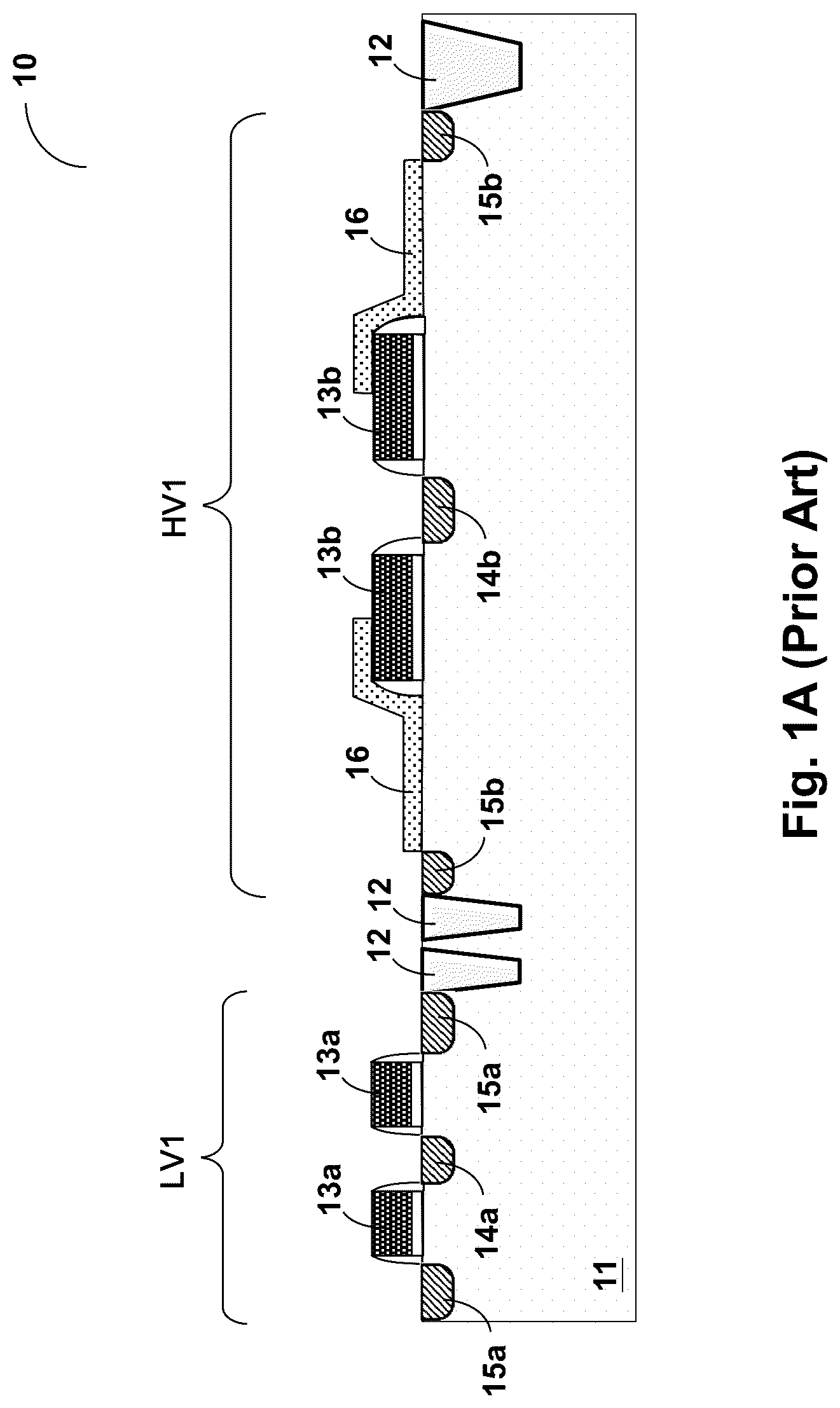
Please refer to A- 1 E , which are cross-sectional schematic diagrams of a conventional manufacturing method of an integrated structure 10 of semiconductor devices having split gates. As shown in A , first, plural insulating regions 12 are formed to electrically isolate a low-voltage device LV 1 and a high-voltage device HV 1 on a substrate 11 . Two low-voltage gates 13 a of the low-voltage device LV 1 are formed on the substrate 11 , and a common low-voltage source 14 a and two low-voltage drains 15 a of the low-voltage device LV 1 are formed in the substrate 11 . On the other hand, two high-voltage gates 13 b and two reduced surface field (RESURF) oxide regions 16 of the high-voltage device HV 1 are formed on the substrate 11 , and a common high-voltage source 14 b and two high-voltage drains 15 b of the high-voltage device HV 1 are formed in the substrate 11 .
Next, referring to B , a silicon oxide layer 17 is formed on the substrate 11 to cover the low-voltage device LV 1 and the high-voltage device HV 1 . And a metal layer 18 is formed to cover the silicon oxide layer 17 .
Next, referring to C , the silicon oxide layer 17 and the metal layer 18 are etched by an etching process to form two split gates SG 1 respectively positioned on the two reduced surface field oxide regions 16 . The split gate SG 1 includes a silicon oxide region 17 a and a top electrode 18 a.
Please continue referring to C , the split gate SG 1 serves for improving on-resistance and breakdown voltage characteristics of the high-voltage device HV 1 . In the conventional art, the thickness of the silicon oxide region 17 a of the split gate SG 1 generally needs to be at least 600 angstrom (Å). With such thickness, as shown in C , after the aforementioned etching process, in regions of the substrate 11 where the space between the structures is small, such as in the low-voltage device LV 1 between the two low-voltage gates 13 a , the silicon oxide layer 17 cannot be completely removed, so that a residual oxide region 17 ′ will remain as shown in C .
Next, referring to D , a contact etch stop layer (CESL) 19 is formed to cover the low-voltage device LV 1 and the high-voltage device HV 1 .
Next, referring to E , the contact etch stop layer 19 is etched back by an etching process to form plural contact holes, and then plural conductive plugs 21 are formed in the corresponding contact holes.
As indicated by a thick dashed circle in E , the aforementioned residual oxide region 17 ′ blocks the conductive plug 21 from contacting the common low-voltage source 14 a , so that the conductive plug 21 cannot be electrically connected to the low-voltage source 14 a , causing the low-voltage device LV 1 to operate abnormally.
In view of the above, the present invention proposes a manufacturing method of an integrated structure of a semiconductor device with split gates, which can avoid the formation of the residual oxide region 17 ′ and solve the problem that the conductive plug 21 cannot be electrically connected to the low-voltage source 14 a.
SUMMARY OF THE INVENTION
From one perspective, the present invention provides a manufacturing method of an integrated structure of a semiconductor device having split gates, comprising: forming two low-voltage gates of a low-voltage device on a substrate and forming a common low-voltage source and two low-voltage drains of the low-voltage device in the substrate; forming two high-voltage gates and two reduced surface field oxide regions of a high-voltage device on the substrate and forming a common high-voltage source and two high-voltage drains of the high-voltage device in the substrate; forming a first silicon nitride layer covering the low-voltage device and the high-voltage device; etching back the first silicon nitride layer by an etching process to form a residual silicon nitride layer on the substrate between the two adjacent low-voltage gates; forming a silicon oxide layer covering the low-voltage device and the high-voltage device; forming a second silicon nitride layer covering the silicon oxide layer; forming a metal layer covering the second silicon nitride layer; etching the metal layer, the second silicon nitride layer, and the silicon oxide layer by at least one etching process to form two split gates respectively on the two reduced surface field oxide regions, wherein each split gate comprises a split gate top electrode, a split gate silicon nitride region, and a split gate silicon oxide region; forming a contact etch stop layer covering the low-voltage device and the high-voltage device, wherein a material of the contact etch stop layer is silicon nitride; etching the contact etch stop layer by an etching process to form a plurality of contact holes in the contact etch stop layer, wherein the contact hole between the two low-voltage gates exposes at least part of a top surface of the common low-voltage source on the substrate; and forming a plurality of conductive plugs in the corresponding plurality of contact holes, wherein each of the conductive plugs fills in the corresponding contact holes from top to bottom.
In one embodiment, the manufacturing method further includes forming a metal-insulator-polysilicon (MIP) capacitor in the substrate, wherein the MIP capacitor includes: a MIP polysilicon region formed above the substrate; a MIP insulating region formed on and in contact with the MIP polysilicon region and the substrate; a MIP metal region formed on and in contact with the MIP insulating region; wherein the MIP metal region and the split gate top electrode are formed by one same process; wherein the MIP insulating region, the split gate silicon nitride region, and the split gate silicon oxide region are formed by one same process; and wherein the MIP polysilicon region and a high-voltage polysilicon region of the high-voltage gate are formed by one same process.
In one embodiment, a material of the split gate top electrode comprises polysilicon, titanium nitride, tantalum nitride, or tungsten.
In one embodiment, a material used for forming the split gate silicon oxide region comprises tetraethoxysilane (TEOS).
In one embodiment, the split gate silicon oxide region is formed by a high temperature oxidation (HTO) process or a high aspect ratio process (HARP).
In one embodiment, a thickness of the reduced surface field oxide region positioned directly under the split gate is 200 angstrom (Å).
In one embodiment, a thickness of the MIP insulating region ranges from 500 Å to 700 Å.
In one embodiment, a thickness of a low-voltage gate oxide layer of the low-voltage gate ranges from 80 Å to 130 Å.
In one embodiment, a gate driving voltage of the high-voltage gates ranges from 3.3V to 5V.
In one embodiment, a drain driving voltage of the high-voltage gates ranges from 6V to 30V.
In one embodiment, the split gate top electrode is electrically connected to the high-voltage gates or a ground potential.
In one embodiment, a minimum feature size of the integrated structure of the semiconductor device having split gates ranges from 0.05 micrometer (μm) to 0.3 μm.
The objectives, technical details, features, and effects of the present invention will be better understood with regard to the detailed description of the embodiments below, with reference to the attached drawings.
BRIEF DESCRIPTION OF THE DRAWINGS
A- 1 E are schematic cross-sectional views illustrating a manufacturing method of an integrated structure 10 of a semiconductor device having split gates according to a conventional art.
A- 2 H are schematic cross-sectional views illustrating a manufacturing method of an integrated structure 50 of a semiconductor device having split gates according to an embodiment of the present invention.
DESCRIPTION OF THE PREFERRED EMBODIMENTS
The drawings as referred to throughout the description of the present invention are for illustration only, to show the interrelations among the process steps and the layers, while the shapes, thicknesses, and widths are not drawn in actual scale.
Referring to A- 2 H , which are schematic cross-sectional views illustrating a manufacturing method of an integrated structure 50 of a semiconductor device having split gates according to an embodiment of the present invention. As shown in A , a substrate 51 is first provided, and two low-voltage gates 53 a of a low-voltage device LV 2 are formed on the substrate 51 , and a common low-voltage source 54 a and two low-voltage drains of the low-voltage device LV 2 are formed in the substrate 51 . In addition, two high-voltage gates 53 b and two reduced surface field oxide regions 56 of the high-voltage device HV 2 are formed on the substrate 51 , and a common high-voltage source 54 b and two high-voltage drains 55 b of the high-voltage device HV 2 are formed in the substrate 51 . Furthermore, in one embodiment, preferably, a polysilicon region 53 c of a metal-insulator-polysilicon (MIP) capacitor MIP 1 is formed on the substrate 51 . In one embodiment, the MIP capacitor MIP 1 is for example formed on an insulating region 52 as shown in A , to have better electrical properties.
The substrate 51 is, for example but not limited to, a P-type or N-type semiconductor substrate. Each of the low-voltage gates 53 a and the high-voltage gates 53 b includes a conductive layer, an spacer layer, and a dielectric layer. The dielectric layer is formed on and in contact with an upper surface of the substrate 51 . The conductive layer includes an N-type polysilicon layer or a P-type polysilicon layer. The spacer layer covers outer sides of two sides of the conductive layer. The details of a transistor gate are well known to those skilled in the art, so such details are not redundantly explained here.
The common low-voltage source 54 a , the two low-voltage drains 55 a , the common high-voltage source 54 b , and the two high-voltage drains 55 b for example can be formed by implanting N-type or P-type impurities into their respective defined regions in the form of accelerated ions by an ion implantation process, which is well known to those skilled in the art, so the details are not redundantly explained here.
Next, referring to B , a first silicon nitride layer 57 is formed to cover the low-voltage device LV 2 , the high-voltage device HV 2 , and the MIP capacitor MIP 1 . The first silicon nitride layer 57 can be formed by, for example but not limited to, a deposition process, which is well known to those skilled in the art, so the details are not redundantly explained here.
Next, referring to C , an etching process is performed to etch back the first silicon nitride layer 57 , in a region with relatively small structural space, such as between the two low-voltage gates 53 a shown in C , whereby a residual silicon nitride layer 57 a is formed on the substrate 51 between the two adjacent low-voltage gates 53 a.
Next, referring to D , a silicon oxide layer 58 is formed to cover the low-voltage device LV 2 , the high-voltage device HV 2 , and the MIP capacitor MIP. A second silicon nitride layer 59 is formed to cover the silicon oxide layer 58 , and a metal layer 62 is formed to cover the second silicon nitride layer 59 . The silicon oxide layer 58 , the second silicon nitride layer 59 , and the metal layer 62 can be formed by, for example but not limited to, respective deposition processes, which is well known to those skilled in the art, so the details are not redundantly explained here.
Next, referring to E , the metal layer 62 , the second silicon nitride layer 59 , and the silicon oxide layer 58 are etched by at least one etching process to form two split gates SG 2 respectively on the two reduced surface field oxide regions 56 , wherein the split gate SG 2 includes split gate top electrode 62 a , split gate silicon nitride region 59 a , and split gate silicon oxide region 58 a . In one embodiment, a MIP metal region 62 b and a MIP insulating region of the MIP capacitor MIP 1 are formed by at least one etching process that is the same as the etching process for etching the metal layer 62 , the second silicon nitride layer 59 , and the silicon oxide layer 58 , wherein the MIP insulating region includes a MIP silicon nitride region 59 b and a MIP silicon oxide region 58 b.
That is, the MIP metal region 62 b and the split gate top electrode 62 a are formed by one same process. The MIP insulating region, the split gate silicon nitride region 59 a , and the split gate silicon oxide region 59 a are formed by one same process. The MIP polysilicon region 53 c and the high-voltage polysilicon region of the high-voltage gate 53 b are formed by one same process. The MIP polysilicon region 53 c is formed above the substrate 51 ; the MIP insulating region is formed on and in contact with the MIP polysilicon region 53 c and the substrate 51 ; and the MIP metal region 62 b is formed on and in contact with the MIP insulating region, wherein a part of the MIP insulating region is formed on and in contact with the MIP polysilicon region 53 c , and another part of the MIP insulating region is formed and in contact with the substrate 51 .
Next, referring to F , a contact etch stop layer 63 is formed to cover the low-voltage device LV 2 , the high-voltage device HV 2 , and the MIP capacitor MIP 1 , wherein the contact etch stop layer 63 is made of silicon nitride.
Next, referring to G , the contact etch stop layer 63 is etched by an etching process, so that plural contact holes 61 ′ are formed in the contact etch stop layer 63 , and the contact hole 61 ′ between the two low-voltage gates 53 a exposes at least part of the top surface of the common low-voltage source 54 a on the substrate 51 . The etching process for etching the contact etch stop layer 63 may include an over-etch step, so that the conductive plugs to be formed later can form better electrical contact with the contact surface.
Next, referring to H , plural conductive plugs 61 are formed in the corresponding plural contact holes 61 ′, and each conductive plug 61 fills the corresponding contact hole 61 ′ from top to bottom thoroughly.
One of the differences between the present invention and the conventional art is that before depositing the silicon oxide layer, the first silicon nitride layer 57 is deposited first. After the first silicon nitride layer 57 is etched back, a residual silicon nitride layer is formed on the substrate 51 where the structural space is relatively small. Since the material of the etch stop layer for the subsequent etching of the contact hole is also silicon nitride, the residual silicon nitride layer can be totally removed, so that the conductive plug will not be blocked from the residual silicon oxide, and the conductive plug can be electrically connected to a desired electric node, such as the common low-voltage source 54 a , in a region where the structural space is relatively small.
In one embodiment, the material of the split gate top electrode 62 a includes polysilicon, titanium nitride, tantalum nitride, or tungsten.
In one embodiment, the material used to form the split gate silicon oxide region 57 a includes tetraethoxysilane (TEOS).
In one embodiment, the split gate silicon oxide region 57 a is formed by a high temperature oxidation (HTO) process or a high aspect ratio process (HARP).
In one embodiment, the thickness of the reduced surface field oxide regions 56 directly under the split gate SG 2 is 200 Å.
In one embodiment, the thickness of the MIP insulating region ranges from 500 Å to 700 Å.
In one embodiment, the thickness of the low-voltage gate oxide layer of the low-voltage gate 53 a ranges from 80 Å to 130 Å.
In one embodiment, a gate driving voltage of the high-voltage gate 53 b ranges from 3.3V to 5V.
In one embodiment, a drain driving voltage of the high-voltage gate 53 b ranges from 6V to 30V.
In one embodiment, the split gate top electrode 62 a is electrically connected to the high-voltage gate 53 b or the ground potential.
In one embodiment, a minimum feature size of the integrated structure 50 of the semiconductor device with the split gate ranges from 0.05 microns to 0.3 microns.
The present invention has been described in considerable detail with reference to certain preferred embodiments thereof. It should be understood that the description is for illustrative purpose, not for limiting the broadest scope of the present invention. Those skilled in this art can readily conceive variations and modifications within the spirit of the present invention. The various embodiments described above are not limited to being used alone; two embodiments may be used in combination, or a part of one embodiment may be used in another embodiment. For example, other process steps or structures, such as a deep well region, may be added. For another example, the lithography process step is not limited to the mask technology but it can also include electron beam lithography, immersion lithography, etc. Therefore, in the same spirit of the present invention, those skilled in the art can think of various equivalent variations and various combinations, and there are many combinations thereof, and the description will not be repeated here. The scope of the present invention should include what are defined in the claims and the equivalents.
Figures (13)
Citations
This patent cites (4)
- US6522587
- US9330923
- US10269909
- US2018/0166451