Memory Cells with Three-dimensional Gate Coupling and Methods of Forming Thereof
Abstract
A memory cell including a substrate having a first doped region and a second doped region spaced apart from each other and defining a channel region therebetween, a floating gate including a first end over the channel region and a second end over the first doped region, a control gate including a first portion arranged laterally adjacent to the second end of the floating gate and a second portion arranged over and overlapping the second end of the floating gate, a word line overlapping the channel region, the first end of the floating gate, and the second portion the control gate, a first insulation member separating the floating gate, the control gate and the word line from the substrate; a second insulation member separating the floating gate from the control gate, and a third insulation member separating the floating gate and the control gate from the word line.
Claims (20)
1. A memory cell comprising: a substrate having a first doped region and a second doped region spaced apart from each other and defining a channel region therebetween; a floating gate over the substrate, the floating gate overlapping the first doped region and the channel region, the floating gate including a first end disposed over the channel region and a second end opposite the first end disposed over the first doped region; a control gate over the substrate, the control gate including a first portion arranged laterally adjacent to the second end of the floating gate and a second portion arranged over and overlapping the second end of the floating gate; a word line over the substrate, a first end of the word line arranged over and overlapping the channel region and not overlapping the second doped region, a second end of the word line arranged over and overlapping the first end of the floating gate and the second portion the control gate; a first insulation member on the substrate, the first insulation member separating the floating gate, the control gate and the word line from the substrate; a second insulation member on the floating gate, the second insulation member separating the floating gate from the control gate; and a third insulation member on the substrate, the floating gate and the control gate, a first portion of the third insulation member separating the floating gate and the control gate from the word line and a second portion of the third insulation member separating the word line from the second doped region, wherein the substrate has a first conductivity type and the first and second doped regions have a second conductivity type opposite the first conductivity type.
17. A method of manufacturing a memory cell comprising: providing a substrate having a first doped region and a second doped region spaced apart from each other and defining a channel region therebetween; providing a floating gate over the substrate, the floating gate overlapping the first doped region and the channel region, the floating gate including a first end disposed over the channel region and a second end opposite the first end disposed over the first doped region; providing a control gate over the substrate, the control gate including a first portion arranged laterally adjacent to the second end of the floating gate and a second portion arranged over and overlapping the second end of the floating gate; providing a word line over the substrate, a first end of the word line arranged over and overlapping the channel region and not overlapping the second doped region, a second end of the word line arranged over and overlapping the first end of the floating gate, and the second portion the control gate; providing a first insulation member on the substrate, the first insulation member separating the floating gate, the control gate and the word line from the substrate; providing a second insulation member on the floating gate, the second insulation member separating the floating gate from the control gate; and providing a third insulation member on the substrate, the floating gate and the control gate, a first portion of the third insulation member separating the floating gate and the control gate from the word line and a second portion of the third insulation member separating the word line from the second doped region, wherein the substrate has a first conductivity type and the first and second doped regions have a second conductivity type opposite the first conductivity type.
Show 18 dependent claims
2. The memory cell of claim 1 , wherein the first insulation member overlaps the first doped region and the channel region, the second insulation member overlaps the second end of the floating gate and the first doped region, the second insulation member underlaps the control gate, and the third insulation member overlaps the first end of the floating gate and the control gate.
3. The memory cell of claim 2 , wherein the floating gate partially overlaps the first doped region and partially overlaps the channel region.
4. The memory cell of claim 2 , the second portion of the control gate is wider than the first portion of the control gate.
5. The memory cell of claim 4 , wherein the second end of the floating gate includes a side surface portion and a top surface portion, the side surface portion faces the first portion of the control gate and the top surface portion faces the second portion of the control gate.
6. The memory cell of claim 4 , wherein the second portion of the control gate is disposed over and partially overlaps the channel region.
7. The memory cell of claim 2 , wherein the control gate conformally covers the second end of the floating gate.
8. The memory cell of claim 2 , wherein the second portion of the control gate overlaps more than half of the floating gate.
9. The memory cell of claim 2 , wherein the control gate completely overlaps the first doped region.
10. The memory cell of claim 2 , wherein the word line covers only a portion of the first end of the floating gate.
11. The memory cell of claim 10 , wherein the word line conformally covers a corner of the first end of the floating gate.
12. The memory cell of claim 10 , wherein the word line partially covers the control gate, and the word line conformally covers a corner of the second portion of the control gate.
13. The memory cell of claim 2 , wherein the second insulation member conformally covers the second end of the floating gate.
14. The memory cell of claim 2 , wherein the floating gate, the control gate, and the word line include polysilicon.
15. The memory cell of claim 2 , wherein the second insulation member includes oxide-nitride-oxide (ONO).
16. The memory cell of claim 2 , wherein a side surface of the floating gate faces a side surface of the first portion of the control gate and an upper surface of the floating gate faces a lower surface of the second portion of the control gate.
18. The memory cell of claim 1 , wherein the first portion of the third insulation member separating the floating gate and the control gate from the word line includes a first silicon nitride layer, the first silicon nitride layer disposed in a vertical direction along a side portion of the control gate.
19. The memory cell of claim 1 , wherein the portion of the third insulation member separating the word line from the second doped region includes a second silicon nitride layer, the second silicon nitride layer disposed in a vertical direction along a side portion of the word line such that the word line does not overlap the second doped region.
20. The memory cell of claim 1 , wherein the second doped region includes an interconnect for a contact terminal disposed over the second doped region.
Full Description
Show full text →
TECHNICAL FIELD
Various embodiments relate to memory cells, and more particular, to nonvolatile memory cells and methods of fabricating memory cells.
BACKGROUND
Flash memory is an electronic non-volatile computer storage medium that can be electrically erased and reprogrammed. Flash memory may include a plurality of flash memory cells. One type of flash memory cells is a split gate memory cell. Split gate memory cells have several advantages over other types of flash memory cells such as the stacked gate memory cells. These advantages include lower power consumption, higher injection efficiency, less susceptibility to short channel effects, and over erase immunity. The programming voltage and erase performance of split gate memory cells depend in part on the control gate (CG)-to-floating gate (GF) gate coupling ratio (GCR). However, it is challenging to manufacture a memory cell with a high CG-FG GCR as the manufacturing process may result in damage to the underlying semiconductor material.
SUMMARY
According to various embodiments, there may be provided a memory cell. The memory cell may include a substrate having a first doped region and a second doped region spaced apart from each other and defining a channel region therebetween; a floating gate over the substrate, the floating gate overlapping the first doped region and the channel region, the floating gate including a first end disposed over the channel region and a second end opposite the first end disposed over the first doped region; a control gate over the substrate, the control gate including a first portion arranged laterally adjacent to the second end of the floating gate and a second portion arranged over and overlapping the second end of the floating gate; a word line over the substrate, the word line arranged over and overlapping the channel region, the first end of the floating gate, and the second portion the control gate; a first insulation member on the substrate, the first insulation member separating the floating gate, the control gate and the word line from the substrate; a second insulation member on the floating gate, the second insulation member separating the floating gate from the control gate; and a third insulation member on the floating gate and the control gate, the third insulation member separating the floating gate and the control gate from the word line, wherein the substrate has a first conductivity type and the first and second doped regions have a second conductivity type opposite the first conductivity type.
According to various embodiments, the first insulation member overlaps the first doped region and the channel region, the second insulation member overlaps the second end of the floating gate and the first doped region, the second insulation member underlaps the control gate, and the third insulation member overlaps the first end of the floating gate and the control gate.
According to various embodiments, the floating gate partially overlaps the first doped region and partially overlaps the channel region.
According to various embodiments, the second portion of the control gate is wider than the first portion of the control gate.
According to various embodiments, the second end of the floating gate includes a side surface portion and a top surface portion, the side surface portion faces the first portion of the control gate and the top surface portion faces the second portion of the control gate.
According to various embodiments, the second portion of the control gate is disposed over and partially overlaps the channel region.
According to various embodiments, the control gate conformally covers the second end of the floating gate.
According to various embodiments, the second portion of the control gate overlaps more than half of the floating gate.
According to various embodiments, the control gate completely overlaps the first doped region.
According to various embodiments, the word line covers only a portion of the first end of the floating gate.
According to various embodiments, the word line conformally covers a corner of the first end of the floating gate.
According to various embodiments, the word line partially covers the control gate.
According to various embodiments, the word line conformally covers a corner of the second portion of the control gate.
According to various embodiments, the second insulation member conformally covers the second end of the floating gate.
According to various embodiments, the third insulation member conformally covers the first end of the floating gate and the control gate.
According to various embodiments, the floating gate, the control gate, and the word line include polysilicon.
According to various embodiments, the second insulation member includes oxide-nitride-oxide (ONO).
According to various embodiments, a portion of the third insulation member arranged along a side of the second portion of the control gate includes silicon nitride.
According to various embodiments, a side surface of the floating gate faces a side surface of the first portion of the control gate and an upper surface of the floating gate faces a lower surface of the second portion of the control gate.
According to various embodiments, there may be provided a method of forming a memory cell. The method may include providing a substrate having a first doped region and a second doped region spaced apart from each other and defining a channel region therebetween; providing a floating gate over the substrate, the floating gate overlapping the first doped region and the channel region, the floating gate including a first end disposed over the channel region and a second end opposite the first end disposed over the first doped region; providing a control gate over the substrate, the control gate including a first portion arranged laterally adjacent to the second end of the floating gate and a second portion arranged over and overlapping the second end of the floating gate; providing a word line over the substrate, the word line arranged over and overlapping the channel region, the first end of the floating gate, and the second portion the control gate; providing a first insulation member on the substrate, the first insulation member separating the floating gate, the control gate and the word line from the substrate; providing a second insulation member on the floating gate, the second insulation member separating the floating gate from the control gate; and providing a third insulation member on the floating gate and the control gate, the third insulation member separating the floating gate and the control gate from the word line, wherein the substrate has a first conductivity type and the first and second doped regions have a second conductivity type opposite the first conductivity type.
Additional features for advantageous embodiments are provided in the dependent claims.
BRIEF DESCRIPTION OF THE DRAWINGS
In the drawings, like reference characters generally refer to the same parts throughout the different views. The drawings are not necessarily to scale, emphasis instead generally being placed upon illustrating the principles of the invention. In the following description, various embodiments are described with reference to the following drawings, in which:
shows a simplified cross-sectional view of a memory cell according to various non-limiting embodiments.
shows magnified cross-sectional view of the memory cell of according to various non-limiting embodiments.
shows a further simplified and magnified cross-sectional view of the memory cell of according to various non-limiting embodiments.
shows an operative cross-sectional view of the memory cell of during a programming phase according to various non-limiting embodiments.
shows an operative cross-sectional view of the memory cell of during an erasing phase according to various non-limiting embodiments.
shows a simplified array arrangement of memory cells of according to various non-limiting embodiments.
shows a table including example operative voltages of the memory cell according to various non-limiting embodiments.
shows a simplified three dimensional perspective view of a memory cell according to various non-limiting embodiments.
A to 9 E show simplified cross-sectional views illustrating a method for fabricating a memory cell according to various non-limiting embodiments.
DESCRIPTION
Aspects of the present invention and certain features, advantages, and details thereof, are explained more fully below with reference to the non-limiting examples illustrated in the accompanying drawings. Descriptions of suitable materials, fabrication tools, processing techniques, etc., are omitted so as not to unnecessarily obscure the invention in detail. It should be understood, however, that the detailed description and the specific examples, while indicating aspects of the invention, are given by way of illustration only, and are not by way of limitation. Various substitutions, modifications, additions, and/or arrangements, within the spirit and/or scope of the underlying inventive concepts will be apparent to those skilled in the art from this disclosure.
Approximating language, as used herein throughout the specification and claims, may be applied to modify any quantitative representation that could permissibly vary without resulting in a change in the basic function to which it is related. Accordingly, a value modified by a term or terms, such as “approximately”, “about,” is not limited to the precise value specified. In some instances, the approximating language may correspond to the precision of an instrument for measuring the value. Further, a direction is modified by a term or terms, such as “substantially” to mean that the direction is to be applied within normal tolerances of the semiconductor industry. For example, “substantially parallel” means largely extending in the same direction within normal tolerances of the semiconductor industry and “substantially perpendicular” means at an angle of ninety degrees plus or minus a normal tolerance of the semiconductor industry.
The terminology used herein is for the purpose of describing particular examples only and is not intended to be limiting of the invention. As used herein, the singular forms “a”, “an” and “the” are intended to include the plural forms as well, unless the context clearly indicates otherwise. It will be further understood that the terms “comprise” (and any form of comprise, such as “comprises” and “comprising”), “have” (and any form of have, such as “has” and “having”), “include (and any form of include, such as “includes” and “including”), and “contain” (and any form of contain, such as “contains” and “containing”) are open-ended linking verbs. As a result, a method or device that “comprises,” “has,” “includes” or “contains” one or more steps or elements possesses those one or more steps or elements, but is not limited to possessing only those one or more steps or elements. Likewise, a step of a method or an element of a device that “comprises,” “has,” “includes” or “contains” one or more features possesses those one or more features, but is not limited to possessing only those one or more features. Furthermore, a device or structure that is configured in a certain way is configured in at least that way, but may also be configured in ways that are not listed.
As used herein, the term “connected,” when used to refer to two physical elements, means a direct connection between the two physical elements. The term “coupled,” however, can mean a direct connection or a connection through one or more intermediary elements.
As used herein, the terms “may” and “may be” indicate a possibility of an occurrence within a set of circumstances; a possession of a specified property, characteristic or function; and/or qualify another verb by expressing one or more of an ability, capability, or possibility associated with the qualified verb. Accordingly, usage of “may” and “may be” indicates that a modified term is apparently appropriate, capable, or suitable for an indicated capacity, function, or usage, while considering that in some circumstances the modified term may sometimes not be appropriate, capable or suitable. For example, in some circumstances, an event or capacity can be expected, while in other circumstances the event or capacity cannot occur—this distinction is captured by the terms “may” and “may be.”
The embodiments generally relate to memory cells. More particularly, some embodiments relate to flash memory devices, and split-gate non-volatile memory cells.
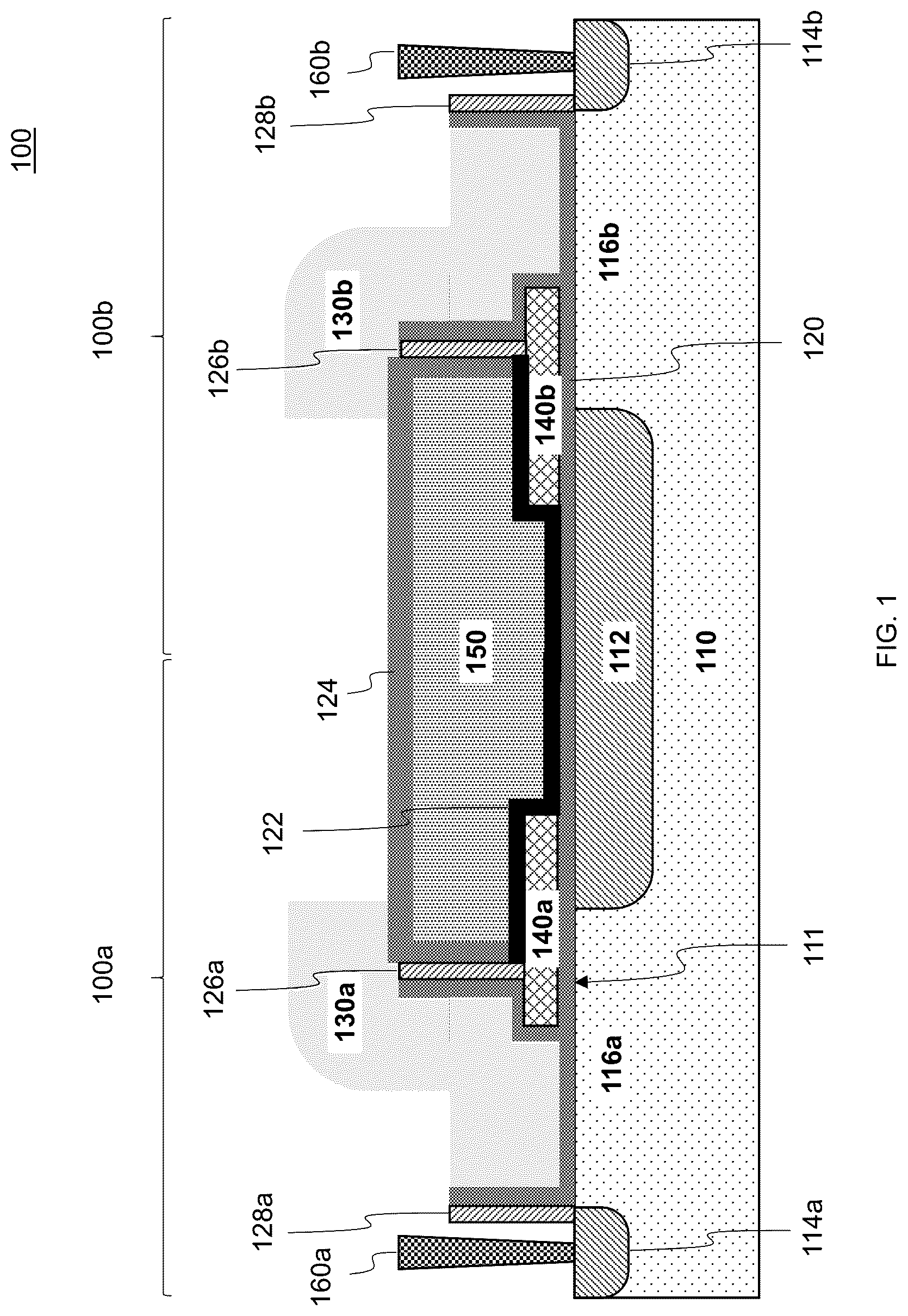
shows a simplified cross-sectional view of a memory cell 100 according to various non-limiting embodiments.
Referring to , the memory cell 100 includes a first memory unit 100 a and a second memory unit 100 b . As shown in , the first memory unit 100 a may include a substrate 110 including a plurality of doped regions. The plurality of doped regions includes a first doped region 112 and a second doped region 114 a . The first doped region 112 and the second doped region 114 a may be spaced apart from each other, and may define a channel region 116 a between them. The substrate 110 may have an upper surface 111 . The first doped region 112 and the second doped region 114 a may be provided along the upper surface 111 of the substrate 110 . The first doped region 112 may serve as a select line (SL) for the first memory unit 100 a . The second doped region 114 a may serve as a contact for a bit line (BL) for the first memory unit 100 a.
The substrate 110 may be formed from a semiconductor. The substrate 110 , for example, may be a silicon substrate. The substrate 110 may also be a silicon germanium, germanium, gallium arsenide, or crystal-on-insulator (COI) such as silicon-on-insulator (SOI) substrate. The substrate 110 may be an undoped substrate. In some embodiments, for example, the substrate 110 may be lightly doped with p-type dopants. In some embodiments, the substrate 110 may be provided with other types of dopants or dopant concentrations.
The substrate 110 may have a first conductivity type. The first doped region 112 and the second doped region 114 a may have a second conductivity type that is different from the first conductivity type. The first conductivity type and the second conductivity type may be opposite conductivity types. For example, the second conductivity type may be p-type while the first conductivity type may be n-type, or vice-versa. The first doped region 112 and the second doped region 114 a may be formed in the substrate 110 by implanting those regions of the substrate 110 with dopants of the second conductivity type.
The first memory unit 100 a may further include an insulation member 120 disposed on the surface 111 of the substrate 110 . The insulation member 120 may cover the first doped region 112 and the channel region 116 a . The insulation member 120 may not cover the second doped region 114 a . The insulation member 120 may extend continuously from the first doped region 112 towards the second doped region 114 a . The insulation member 120 may include a dielectric material such as silicon oxide. Other examples of dielectric materials may include, for example, oxides, nitrides, or oxynitrides. The dielectric materials may be high-k dielectric materials, such as, aluminum oxide, hafnium oxide, silicon nitride, silicon oxynitride, or combinations thereof.
The first memory unit 100 a may further include a word line (WL) 130 a , a floating gate (FG) 140 a and a control gate (CG) 150 disposed over the insulation member 120 . The word line 130 a , the floating gate 140 a , and the control gate 150 may be separated from each other by one or more insulation members. The floating gate 140 a may be arranged over and overlapping a portion of the first doped region 112 and a portion of the channel region 116 a . The control gate 150 may be arranged over and overlapping the first doped region 112 , a portion of the floating gate 140 a and a portion of the channel region 116 a . The word line 130 a may be arranged over the channel region 116 a , a portion of the floating gate 140 a and a portion of the control gate 150 . The word line 130 a , the floating gate 140 a and the control gate 150 may be formed from polysilicon, or other semiconductor materials.
shows a magnified cross-sectional view of the memory cell 100 according to various non-limiting embodiments.
Referring to , the floating gate 140 a may further be arranged between the word line 130 a and the control gate 150 . The floating gate 140 a may include a first end 142 and a second end 146 , the second end 146 opposite the first end 142 . The first end 142 may be nearer to the word line 130 a and the second end 146 may be nearer to the control gate 150 . The first end 142 may be arranged over and overlapping the channel region 116 a and the second end 146 may be arranged over and overlapping the first doped region 112 . The first end 142 may further be covered by a portion of the word line 130 a . That is, the first end 142 may include a side portion 143 and a top portion 144 that are covered by the word line 130 a . The word line 130 a may conformally cover the first end 142 of the floating gate 140 a . The second end 146 may be covered by a portion of the control gate 150 . That is, the second end 146 may include a side portion 147 and a top portion 148 that are covered by the control gate 150 . The control gate 150 may conformally cover the second end 146 of the floating gate 140 a.
The control gate 150 may include a lower portion 155 and an upper portion 156 . The upper portion 156 may be wider than the lower portion 155 such that the upper portion 155 protrudes from the lower portion. The upper portion 156 may protrude from the lower portion 155 so as to partially overlap the floating gate 140 a . The upper portion 156 may include an overhang portion 158 that overlaps the floating gate. Referring to , the lower portion 155 of the control gate 150 may be disposed adjacent to the second end 146 of the floating gate 140 a . For example, the lower portion 155 may have a thickness that is substantially similar to a thickness of the floating gate 140 a.
The upper portion 156 of the control gate 150 may further be arranged over the floating gate 140 a to extend along the top portion 148 of the floating gate 140 a . The upper portion 156 may include the overhang portion 158 that is disposed over and overlaps the second end 146 of the floating gate 140 a . The overhang portion 158 may overlap the entire portion of the floating gate 140 a that is disposed over and overlapping the first doped region 112 . The overhang portion 158 of the control gate 150 may further be arranged over the floating gate 140 a to overlap a portion of the floating gate 140 a that is disposed over the channel region 116 a.
The portion of the channel region 116 a underlapping the floating gate 140 a may be adjacent to the first doped region 112 .
Referring to , the word line 130 a may be arranged over the floating gate 140 a to extend along the top portion 144 of the floating gate 140 a . The word line 130 a may overlap the first end 142 of the floating gate 140 a . The word line 130 a may overlap a substantial or the entire portion of the floating gate 140 a that is disposed over the channel region 116 a . In various embodiments, the word line 130 a may further be arranged over the floating gate 140 a and control gate 150 to partially overlap the overhang portion 158 of the control gate 150 that is disposed over the channel region 116 a . In various embodiments, the word line 130 a may further be disposed over a portion of the first doped region 112 .
In various embodiments, at least half of the floating gate 140 a may be disposed over the first doped region 112 . In various embodiments, the control gate 150 may be disposed over more than at least half of the floating gate 140 a.
The word line 130 a , floating gate 140 a , control gate 150 and substrate 110 may be separated from each other by one or more insulation members, including insulation member 120 . The insulation member 120 may insulate the floating gate 140 a from the second doped region 114 a and the channel region 116 a . The insulation member 120 may further insulate the floating gate 140 a from the channel region 116 a and the first doped region 112 . The insulation member 120 may further insulate the control gate 150 from the first doped region 112 . The insulation member 120 may be made from insulator material including one of silicon oxide, silicon nitride, silicon oxide stack or combinations thereof.
The first memory unit 100 a may further include a second insulation member 122 disposed over the floating gate 140 a and the insulation member 120 . The second insulation member 122 may insulate the floating gate 140 a from the control gate 150 . For example, the second insulation member 122 may be arranged to overlap and cover the second end 146 of the floating gate 140 a . The second insulation member 122 may conformally cover a side portion 147 and a top portion 148 of the floating gate 140 a . The second insulation member 122 may be a multilayer dielectric. For example, the second insulation member 122 may include an oxide-nitride-oxide (ONO).
The first memory unit 100 a may further include a third insulation member 124 disposed over and overlapping the floating gate 140 a , the control gate 150 and a portion of the insulation member 120 . The third insulation member 124 insulates the control gate 150 and the floating gate 140 a from the word line 130 a . For example, the third insulation member 124 may be arranged to cover the first end 142 of the floating gate 140 a . The third insulation member 124 may cover a side portion 143 and a top portion 144 of the floating gate 140 a . For example, the third insulation member 124 may be arranged to further conformally cover the control gate 150 . That is, part of the third insulation member 124 may insulate the floating gate 140 a from the word line 130 a . Another part of the third insulation member 124 may insulate the word line 130 a from the control gate 150 . A further part of the third insulation member 124 may insulate the word line 130 a from the second doped region 114 a.
The third insulation member 124 may include a dielectric material such as silicon oxide. At least a portion of the third insulation member 124 may be a multilayer dielectric. For example, the portion of the third insulation member 124 separating the word line 130 a from the side portion 152 of the control gate 150 may further include a silicon nitride layer 126 a extending vertically along the side portion 152 between two silicon oxide layers. For another example, the portion of the third insulation member 124 separating the word line 130 a from the second doped region 114 a may further include a silicon nitride layer 128 a adjacent to the silicon oxide layer both extending vertically along a side portion of the word line 130 a.
In various embodiments, the insulation members may include dielectric materials, for example oxides, nitrides, or oxynitrides. The dielectric materials may be high-k dielectric materials such as aluminum oxide, hafnium oxide, silicon nitride, silicon oxynitride, or combinations thereof. In various embodiments, the word line 130 a , the floating gate 140 a and the control gate 150 may be formed from polysilicon, or other semiconductor materials.
Referring to which shows a magnified view of the first memory unit 100 a , the floating gate 140 a may have a tip formed at the corner of the first end 142 where the side portion 143 and the top portion 144 meet. In various embodiments, the side portion 143 and top portion 144 may meet at a substantially perpendicular angle. In other various embodiments, the side portion 143 may incline towards the top portion 144 . The word line 140 a may conformally cover the first end 142 of the floating gate 140 a.
Referring to , the second doped region 114 a may include an interconnect for a contact terminal (CT) 160 a disposed over the second doped region 114 a . The interconnect 160 a may include a metal. The interconnect may be in direct contact with the second doped region 114 a . The interconnect 160 a may be separated from the word line 130 a by a portion of the third insulation member 124 . The interconnect 160 a may further be separated from the word line 130 a by a further insulation member 128 a . The further insulation member 128 a may include silicon nitride. The second doped region 114 a may be electrically coupled to a bit line.
The second memory unit 100 b of memory cell 100 is substantially a mirrored version of the first memory unit 100 a . The first doped region 112 (e.g., select line) and control gate 150 are common to the first memory unit 100 a and the second memory unit 100 b.
shows a further magnified and simplified view of the first memory unit 100 a according to various non-limiting embodiments. For example, referring to , the control gate 150 may include a lower portion 155 having a length 155 x and a height 155 y and an upper portion 156 having a length 156 x and a height 158 y . The upper portion 156 may be wider than the lower portion 155 such that the upper portion 155 protrudes from the lower portion. The upper portion 156 may protrude from the lower portion 155 so as to partially overlap the floating gate 140 a . The upper portion 156 that overlaps the floating gate 106 may be referred herein as the overhang portion 158 of the control gate 150 . The overhang portion 156 may have a length 158 x.
For example, referring to , the height 140 y of the floating gate and the height 155 y of the lower portion 155 of the control gate 150 may be substantially the same. The length 140 x of the floating gate may be greater than the length 158 x of the overhang portion 158 of the control gate 150 . The length 155 x of the lower portion 155 of the control gate 150 may be greater than the length 158 x of the overhang portion 158 of the control gate 150 . The height 158 y of the overhang portion 158 and upper portion 156 of the control gate 150 may be greater than the height 155 y of the lower portion 155 of the control gate 150 .
shows a simplified logical schematic illustrating the connections for an array of memory cells 100 . Each of the dashed boxes includes a memory cell 100 . For example, with respect to memory cell 100 - 1 , the first doped region 112 may be connected to SL 0 , the control gate 150 may be connected to CG 0 , the second doped region 114 a may be connected to BL 0 , the second doped region 114 b may be connected to BL 0 , the word line 130 a may be connected to WL 0 , the word line 130 b may be connected to WL 1 . For example, with respect to memory cell 100 - 2 , the first doped region 112 may be connected to SL 0 , the control gate 150 may be connected to CG 0 , the second doped region 114 a may be connected to BL 1 , the second doped region 114 b may be connected to BL 1 the word line 130 a may be connected to WL 0 , the word line 130 b may be connected to WL 1 . And connections are similarly made with regards to memory cells 100 - 3 and 100 - 4 . For example, with respect to memory cell 100 - 5 , the first doped region 112 may be connected to SL 1 , the control gate 150 may be connected to CG 1 , the second doped region 114 a may be connected to BL 0 , the second doped region 114 b may be connected to BL 0 , the word line 130 a may be connected to WL 2 , the word line 130 b may be connected to WL 3 . For example, with respect to memory cell 100 - 6 , the first doped region 112 may be connected to SL 1 , the control gate 150 may be connected to CG 1 , the second doped region 114 a may be connected to BL 1 , the second doped region 114 b may be connected to BL 1 , the word line 130 a may be connected to WL 2 , the word line 130 b may be connected to WL 3 . And connections are similarly made with regards to memory cells 100 - 7 and 100 - 8 .
shows an operative cross-sectional view of the memory cell of during a programming phase according to various non-limiting embodiments.
shows an operative cross-sectional view of the memory cell of during an erasing phase according to various non-limiting embodiments.
shows a simplified array arrangement of memory cells of according to various non-limiting embodiments.
shows a table including example operative voltages of the memory cell according to various non-limiting embodiments.
Referring to , the memory cell unit 100 a is in programming mode when the first doped region 112 (SL) is at 6V, the word line 130 a (WL) is at 1.5 V, the control gate (CG) 150 is at 8V, and the second doped region 114 a (BL) is at 2.5V. During the programming mode, there is a voltage differential between the control gate 150 and the bit line 114 a via the floating gate 140 a , the voltage of the control gate turns the floating gate 140 a conductive, and the floating gate 140 a stores electrons received from the channel 116 a . The floating gate 140 a is set to the same voltage as the control gate.
Referring to , the memory cell unit 100 a is in erase mode when the first doped region 112 (SL) is at 0 V, the word line 130 a (WL) is at 8 V, the control gate (CG) 150 is at −8V, and the second doped region 114 a (BL) is at 0 V. During the erase mode, there is a voltage differential between the control gate 150 and the word line 130 a via the floating gate 140 a , the voltage of the control gate turns the floating gate 140 a conductive, and the stored electrons in the floating gate 140 a is discharged through the word line 130 a . The floating gate 140 a is set to 2.5V, the same voltage as the word line 130 a.
shows a simplified 3D perspective view of a memory cell according to various non-limiting embodiments. shows only the control gate 150 and the floating gate 140 a and 140 b and their relationship to each other. As shown in , the control gate 150 is adjacent to and/or overlaps the floating gate 140 a in the X-direction, Y-direction, and Z-direction (three-dimensions). That is, two surfaces of the control gate are opposite two surfaces of the floating gate. The improved CG to FG GCR (gate coupling ratio) facilitates a lower programming voltage of 8V instead of 11.5V in a conventional memory cell unit, thus enhancing PGM efficiency. The higher GCR (gate coupling ratio) is facilitated by maximizing CG/SL overlap with FG. The erase performance may also be enhanced by minimizing WL to FG overlap and applying negative voltage on CG.
A to 9 E show simplified cross-sectional views illustrating a method for fabricating the memory cell 100 according to various non-limiting embodiments. For clarity of illustration, some reference numerals are omitted from A to 9 E .
Referring to A , a first doped region 112 and two second doped regions 114 a and 114 b may be formed in the substrate 110 using suitable implanting techniques. For example, a 5V deep Nwell, a HV Nwell, and a HV Pwell may be provided. A deep Nwell may allow negative voltage usage. Further, an NVM pwell and SL implant may be provided. An insulation member 120 may then be formed over the substrate 110 using suitable techniques, e.g., silicon oxide deposition via CVD. For example, the insulation member 120 may be formed on the upper surface 111 of the substrate 110 . Two floating gates 140 a and 140 b may be formed over and on the insulation member 120 so that each floating gate overlaps an end portion of the first doped region 112 . The floating gates 140 a and 140 b may be spaced apart from each other such that there is a gap therebetween. The floating gates may be formed using suitable techniques, e.g., floating gate mask patterning, polysilicon implanting and annealing.
Referring to B , a second insulation member 122 may be provided over each floating gate 140 a and 140 b and the space therebetween. The second insulation member 122 may continuously extend from floating gate 140 a to floating gate 140 b . The second insulation member 122 may include an insulating material such as one of silicon dioxide, silicon nitride, or combination thereof. The second insulation member 122 may conformally cover and overlap an end of each of the floating gates 140 a and 140 b . The insulation member 122 may be formed using suitable techniques, e.g., ONO deposit and ONO anneal.
Referring to C , a control gate 150 may be formed over the insulation member 122 so that the control gate 150 may overlap the floating gates. A lower portion 155 of the control gate 150 is disposed between the floating gates 140 a and 140 b and an upper portion 156 of the control gate 150 includes overhang portions 158 a , 158 b that overlap an end of each of the floating gates 140 a , 140 b , respectively. Each floating gate 140 a and 140 b may be insulated from the control gate 150 by the second insulation member 122 . The control gate 150 may be formed using suitable techniques, e.g., control gate mask patterning, polysilicon implanting and annealing.
Referring to D , a third insulation member 124 may be formed over the floating gates 140 a , 140 b and the control gate 150 using suitable techniques. The process may include depositing an insulating material, such as an oxide onto the floating gates and the control gate and growing the insulation material through an oxidation process. A portion of the third insulation member 124 may further include a silicon nitride layer 126 a , 126 b extending vertically along a side portion 152 of the control gate 150 . The silicon nitride layer may be formed between two silicon oxide layers. A second portion of the third insulation member 124 may also further include a silicon nitride layer 128 a , 128 b extending vertically from the second doped region 114 and along a bit line contact terminal 160 . The multilayer portions of the third insulation member 124 may be formed using suitable techniques.
Referring to E , word lines 130 a and 130 b may be formed on the third insulation member 124 covering the floating gates 140 a , 140 b and control gate 150 to form the memory cell 100 . The word lines may be formed using suitable techniques, e.g., word line mask, polysilicon implant and annealing. Each word line 130 may be continuous and include a first horizontal segment 131 , a vertical segment 133 , and a second horizontal segment 135 . Each word line 130 a , 130 b may conformally cover and overlap a portion of a channel region 116 a , 116 b , an end 142 of a floating gate 140 a , 140 b , and an end of a control gate 150 . The first horizontal segment 131 may cover a portion of the channel region. The vertical segment 133 may cover side portion 143 and top portion 144 at an end 142 of the floating gate 140 and a side portion 152 of the control gate 150 . The second horizontal segment 135 may cover a top portion at an end of the control gate 150 .
A logic device (not shown) may also be fabricated onto the semiconductor structure.
The invention may be embodied in other specific forms without departing from the spirit or essential characteristics thereof. The foregoing embodiments, therefore, are to be considered in all respects illustrative rather than limiting the invention described herein. Scope of the invention is thus indicated by the appended claims, rather than by the foregoing description, and all changes that come within the meaning and range of equivalency of the claims are intended to be embraced therein.
Figures (11)
Citations
This patent cites (7)
- US5242848
- US6103573
- US6133097
- US6566707
- US6747310
- US2015/0372121
- US2021/0036117