System and Semiconductor Device Therein
Abstract
A system includes a measuring device, a processing device and a signal generating device. The measuring device is configured to measure a voltage difference between a first node and a second node. The processing device is coupled between the first node and the second node. The signal generating device is configured to provide a first clock signal to the processing device to adjust the voltage difference, configured to generate the first clock signal according to a first enable signal and a second clock signal, and configured to align an edge of the first enable signal with an edge of the second clock signal. A method and a device are also disclosed herein.
Claims (20)
1. A system, comprising: a measuring device configured to measure a voltage difference; and a signal generating device configured to adjust the voltage difference according to a first enable signal, configured to divide a first clock signal to generate a second enable signal, and configured to delay the second enable signal to generate the first enable signal, wherein the signal generating device comprises a first flip flop, a data input terminal of the first flip flop is configured to receive the first clock signal, and a clock input terminal of the first flip flop is configured to receive the first enable signal.
8. A method, comprising: generating a first enable signal according to a first clock signal; receiving the first clock signal by a gating circuit; triggering the gating circuit by the first clock signal; aligning a first edge of the first clock signal with a second edge of the first enable signal; and receiving the first clock signal and a second enable signal by a logic element in the gating circuit, wherein the first enable signal is different from the second enable signal.
16. A device, comprising: a delaying circuit configured to receive a first enable signal and a controlling signal to generate a second enable signal; a controlling circuit configured to generate the controlling signal according to a feedback signal, to adjust a delay time period between the first enable signal and the second enable signal; and a detecting circuit configured to be triggered by the second enable signal to generate the feedback signal, wherein the controlling circuit is further configured to add a logic value of the feedback signal to an accumulated value, and adjust the controlling signal according to the accumulated value.
Show 17 dependent claims
2. The system of claim 1 , wherein the signal generating device comprises: a gating circuit configured to be triggered by the first clock signal to generate a gated clock signal according to the first enable signal, wherein the voltage difference is adjusted according to the gated clock signal.
3. The system of claim 2 , wherein the gating circuit comprises: a second flip flop, wherein a data input terminal of the second flip flop is configured to receive the first enable signal, and a clock input terminal of the second flip flop is configured to receive the first clock signal.
4. The system of claim 3 , wherein the gating circuit comprises: a logic element configured to output the gated clock signal, a first input terminal of the logic element is coupled to an output terminal of the second flip flop, and a second input terminal of the logic element is configured to receive the first clock signal.
5. The system of claim 1 , wherein the signal generating device comprises: a delaying circuit configured to generate the first enable signal according to a feedback signal; and a detecting circuit generate the feedback signal according the first enable signal and the first clock signal.
6. The system of claim 5 , wherein the first flip flop is configured to output the feedback signal.
7. The system of claim 1 , wherein the signal generating device is further configured to align an edge of the first clock signal and an edge of the first enable signal.
9. The method of claim 8 , further comprising: generating a gated clock signal by the gating circuit; adjusting a voltage difference according to the gated clock signal; and sensing the voltage difference when the gated clock signal oscillates.
10. The method of claim 8 , further comprising: generating a feedback signal according to the first clock signal and the second edge; and adjusting the first enable signal according to the feedback signal.
11. The method of claim 10 , wherein in response to the first clock signal having a first voltage level at a moment of the second edge, the feedback signal has a first logic value, in response to the first clock signal having a second voltage level at the moment of the second edge, the feedback signal has a second logic value, the first voltage level is different from the second voltage level, and the first logic value is different from the second logic value.
12. The method of claim 10 , further comprising: adding a first logic value of the feedback signal to an accumulated value; comparing the accumulated value with a first threshold value; and in response to the accumulated value being smaller than or equal to the first threshold value, resetting the accumulated value.
13. The method of claim 12 , further comprising: generating a controlling signal according to the feedback signal; adjusting the first enable signal according to the controlling signal; and in response to the accumulated value being larger than the first threshold value, increasing a digital value of the controlling signal.
14. The method of claim 13 , further comprising: after the accumulated value is reset, detecting the first clock signal to generate the feedback signal; adding a second logic value of the feedback signal to the accumulated value; comparing the accumulated value with a second threshold value; and in response to the accumulated value being smaller than the second threshold value, increasing the digital value of the controlling signal.
15. The method of claim 14 , wherein the second threshold value is smaller than the first threshold value.
17. The device of claim 16 , wherein the delaying circuit comprises: a converter configured to generate a third enable signal and a fourth enable signal according to the controlling signal; a first delaying unit configured to delay the first enable signal and configured to turned on according to the third enable signal; a second delaying unit configured to delay the first enable signal and configured to turned on according to the fourth enable signal; and a first inverter coupled to the first delaying unit and configured to output the second enable signal.
18. The device of claim 17 , wherein the first delaying unit comprises a second inverter, a third inverter and a fourth inverter, the second delaying unit comprises a fifth inverter and a sixth inverter, an input terminal of the second inverter is configured to receive the first enable signal, an output terminal of the second inverter, an input terminal of the third inverter and an input terminal of the fifth inverter are coupled to each other, an output terminal of the third inverter, an output terminal of the sixth inverter and an input terminal of the fourth inverter are coupled to each other, and an output terminal of the fourth inverter is coupled to an input terminal of the first inverter.
19. The device of claim 16 , wherein the delaying circuit comprises: a converter configured to generate a third enable signal according to the controlling signal; a first inverter configured to receive the third enable signal; a plurality of logic elements, a first input terminal of the plurality of logic elements being coupled to an output terminal of the first inverter; and a plurality of first inverters configured to output the second enable signal, an output terminal of the plurality of logic elements being coupled to an input terminal of the plurality of first inverters.
20. The device of claim 19 , wherein the delaying circuit further comprises: a plurality of second inverters configured to receive the first enable signal, an output terminal of the plurality of second inverters being coupled a second input terminal of the plurality of logic elements.
Full Description
Show full text →
RELATED APPLICATION
This application is a continuation Application of U.S. application Ser. No. 17/828,834, filed May 31, 2022, which is herein incorporated by reference.
BACKGROUND
A power delivery network transforms input voltage signals between various power domains to generate reference voltage signals. The reference voltage signals provide electric power to various devices for operations. A measurement to an impedance of the power delivery network is performed with a current sink. The current sink occupies large on-chip area and may induce a leakage current.
BRIEF DESCRIPTION OF THE DRAWINGS
Aspects of the present disclosure are best understood from the following detailed description when read with the accompanying figures. It is noted that, in accordance with the standard practice in the industry, various features are not drawn to scale. In fact, the dimensions of the various features may be arbitrarily increased or reduced for clarity of discussion.
is a schematic diagram of a system in accordance with some embodiments of the present disclosure.
A is a schematic diagram of the gating circuit shown in , in accordance with some embodiments of the present disclosure.
B is a schematic diagram of the detecting circuit shown in , in accordance with some embodiments of the present disclosure.
is a timing diagram associated with operations of the signal generating device shown in , in accordance with some embodiments of the present disclosure.
A is a flowchart diagram of operations of the system shown in , in accordance with some embodiments of the present disclosure.
B is a flowchart diagram of operations of the signal generating device shown in , in accordance with some embodiments of the present disclosure.
A is a timing diagram of the clock signal shown in , in accordance with some embodiments of the present disclosure.
B is a timing diagram of the clock signal, the enable signals and the feedback signal shown in , in accordance with some embodiments of the present disclosure.
C is a timing diagram of the clock signal, the enable signals, and the feedback signal shown in , in accordance with some other embodiments of the present disclosure.
D is a timing diagram of the clock signal, the enable signals, and the feedback signal shown in , in accordance with various embodiments of the present disclosure.
is a schematic diagram of the delaying circuit corresponding to the delaying circuit shown in , in accordance with some embodiments of the present disclosure.
is a timing diagram associated with operations of the delaying circuit shown in , in accordance with some embodiments of the present disclosure.
is a schematic diagram of the delaying circuit corresponding to the delaying circuit shown in , in accordance with some embodiments of the present disclosure.
A is a schematic diagram of a system corresponding to the system shown in , in accordance with some embodiments of the present disclosure.
B is a timing diagram associated with operations of the system shown in A , in accordance with some embodiments of the present disclosure.
DETAILED DESCRIPTION
The following disclosure provides many different embodiments, or examples, for implementing different features of the provided subject matter. Specific examples of components, materials, values, steps, arrangements or the like are described below to simplify the present disclosure. These are, of course, merely examples and are not intended to be limiting. Other components, materials, values, steps, arrangements or the like are contemplated. For example, the formation of a first feature over or on a second feature in the description that follows may include embodiments in which the first and second features are formed in direct contact, and may also include embodiments in which additional features may be formed between the first and second features, such that the first and second features may not be in direct contact. In addition, the present disclosure may repeat reference numerals and/or letters in the various examples. This repetition is for the purpose of simplicity and clarity and does not in itself dictate a relationship between the various embodiments and/or configurations discussed.
Further, spatially relative terms, such as “beneath,” “below,” “lower,” “above,” “upper” and the like, may be used herein for ease of description to describe one element or feature's relationship to another element(s) or feature(s) as illustrated in the figures. The spatially relative terms are intended to encompass different orientations of the device in use or operation in addition to the orientation depicted in the figures. The device may be otherwise oriented (rotated 90 degrees or at other orientations) and the spatially relative descriptors used herein may likewise be interpreted accordingly. The term mask, photolithographic mask, photomask and reticle are used to refer to the same item.
The terms applied throughout the following descriptions and claims generally have their ordinary meanings clearly established in the art or in the specific context where each term is used. Those of ordinary skill in the art will appreciate that a component or process may be referred to by different names. Numerous different embodiments detailed in this specification are illustrative only, and in no way limits the scope and spirit of the disclosure or of any exemplified term.
It is worth noting that the terms such as “first” and “second” used herein to describe various elements or processes aim to distinguish one element or process from another. However, the elements, processes and the sequences thereof should not be limited by these terms. For example, a first element could be termed as a second element, and a second element could be similarly termed as a first element without departing from the scope of the present disclosure.
In the following discussion and in the claims, the terms “comprising,” “including,” “containing,” “having,” “involving,” and the like are to be understood to be open-ended, that is, to be construed as including but not limited to. As used herein, instead of being mutually exclusive, the term “and/or” includes any of the associated listed items and all combinations of one or more of the associated listed items.
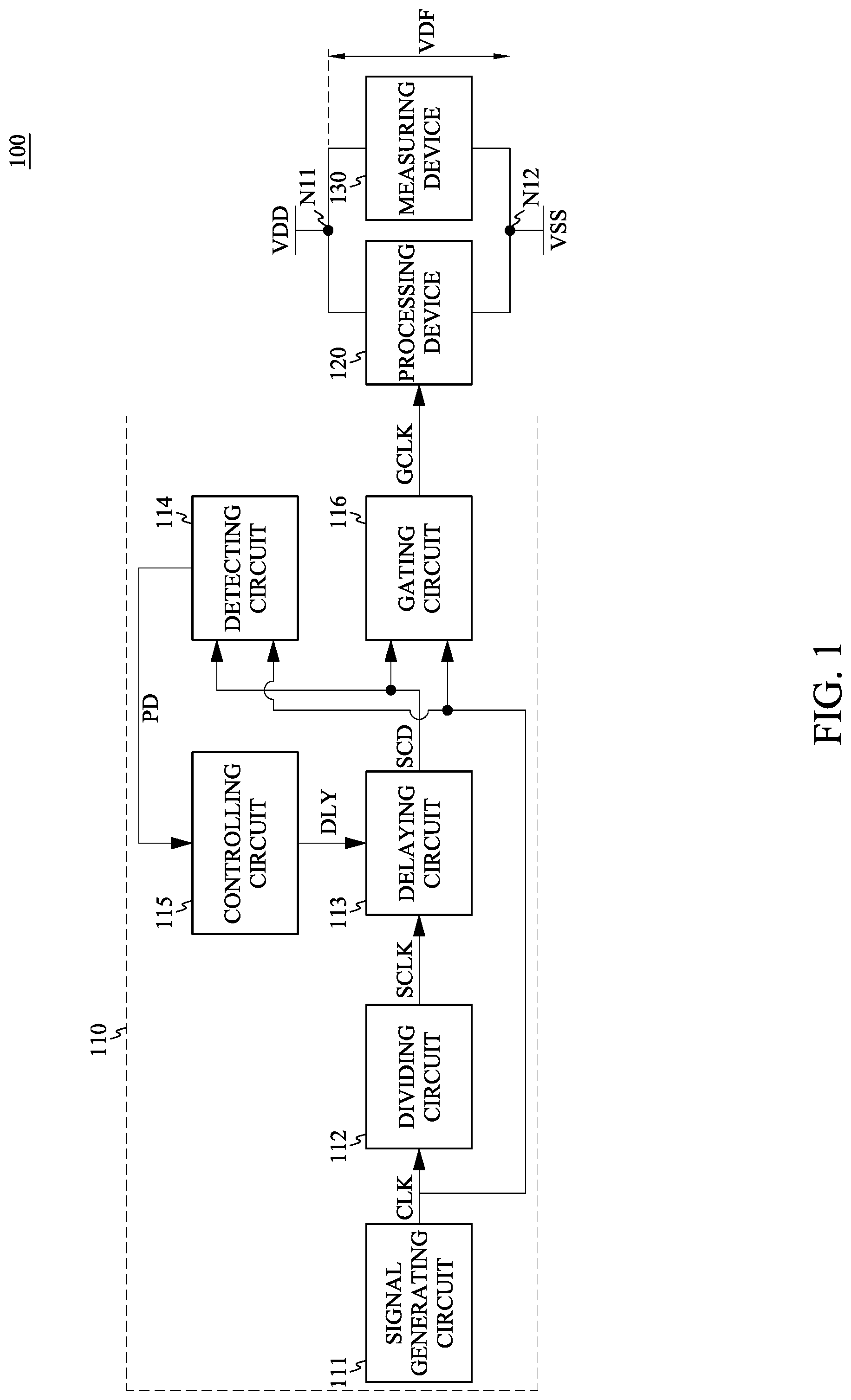
is a schematic diagram of a system 100 in accordance with some embodiments of the present disclosure. In some embodiments, the system 100 includes a signal generating device 110 , a processing device 120 and a measuring device 130 . As illustratively shown in , the processing device 120 is configured to receive a reference voltage signal VDD at a node N 11 and receive a reference voltage signal VSS at a node N 12 to operate. The measuring device 130 is coupled to the nodes N 11 and N 12 , and configured to measure a voltage difference VDF between the nodes N 11 and N 12 , to extract an impedance of a power delivery network (not shown in ) which is configured to provide the reference voltage signals VSS and VDD. The signal generating device 110 is configured to apply a gated clock signal GCLK to the processing device 120 to adjust the voltage difference VDF.
In some embodiments, the processing device 120 is implemented by a central processing unit (CPU), a high-performance computing (HPC) device, or other suitable device. In some embodiments, the measuring device 130 is implemented by an on-chip probe, an edge detector, or other suitable device.
In some embodiments, the signal generating device 110 includes a signal generating circuit 111 , a dividing circuit 112 , a delaying circuit 113 , a detecting circuit 114 , a controlling circuit 115 and a gating circuit 116 .
As illustratively shown in , the signal generating circuit 111 is configured to generate a clock signal CLK. The dividing circuit 112 is configured to receive the clock signal CLK, and divide a frequency of the clock signal CLK to generate an enable signal SCLK. The delaying circuit 113 is configured to delay the enable signal SCLK to generate an enable signal SCD. The detecting circuit 114 is configured to generate a feedback signal PD according to the clock signal CLK and the enable signal SCD. The controlling circuit 115 is configured to generate a controlling signal DLY according to the feedback signal PD, to control the delaying circuit 113 . The gating circuit 116 is configured to generate the gated clock signal GCLK according to the clock signal CLK and the enable signal SCD.
In some embodiments, the signal generating circuit 111 is implemented by a phase locked loop circuit. The dividing circuit 112 is implemented by a divider. The delaying circuit 113 is implemented by a digital controlled delay line. The detecting circuit 114 is implemented by a phase detector. The controlling circuit 115 is implemented by a processor. The gating circuit 116 is implemented by an isolation clock gating circuit.
In various embodiments, the gated clock signal GCLK is applied to various devices, such as devices and systems which need accurate start-up timing, devices which need to operate at a specific timing region, devices which need to be powered on or powered off for strict timing requirement without large uncertainty, and systems which need to start at a certain time point, such as a rocket launch system.
A is a schematic diagram of the gating circuit 116 shown in , in accordance with some embodiments of the present disclosure. In some embodiments, the gating circuit 116 includes a flip flop 210 and a logic element 220 .
As illustratively shown in A , a data input terminal (D) of the flip flop 210 is configured to receive the enable signal SCD, a clock input terminal of the flip flop 210 is configured to receive the clock signal CLK, and an output terminal (Q) of the flip flop 210 is configured to output an enable signal GN.
In some embodiments, the flip flop 210 is configured to transmit a logic value of the enable signal SCD to the output terminal of the flip flop 210 , when the clock input terminal of the flip flop 210 is triggered by an edge of the clock signal CLK, to generate the enable signal GN. In some embodiments, the flip flop 210 is configured to invert a logic value and a corresponding voltage value of the clock signal CLK at the clock input terminal of the flip flop 210 .
As illustratively shown in A , a first input terminal of the logic element 220 is configured to receive the enable signal GN, a second input terminal of the logic element 220 is configured to receive the clock signal CLK, and an output terminal of the logic element 220 is configured to output the gated clock signal GCLK. In some embodiments, the logic element 220 is implemented by an AND logic gate.
B is a schematic diagram of the detecting circuit 114 shown in , in accordance with some embodiments of the present disclosure. In some embodiments, detecting circuit 114 includes a flip flop 230 .
As illustratively shown in B , a data input terminal (D) of the flip flop 230 is configured to receive the clock signal CLK, a clock input terminal of the flip flop 230 is configured to receive the enable signal SCD, and an output terminal (Q) of the flip flop 230 is configured to output the feedback signal PD.
In some embodiments, the flip flop 230 is configured to transmit a logic value of the clock signal CLK to the output terminal of the flip flop 230 , when the clock input terminal of the flip flop 230 is triggered by an edge of the enable signal SCD, to generate the feedback signal PD.
is a timing diagram 300 associated with operations of the signal generating device 110 shown in , in accordance with some embodiments of the present disclosure. As illustratively shown in , the timing diagram 300 includes moments T 31 , T 315 , and T 32 -T 34 arranged in order.
As illustratively shown in , before the moment T 31 , the clock signal CLK is adjusted from the voltage level VL to the voltage level VH. The clock signal CLK has the voltage level VH at the moment T 31 . Accordingly, the enable signal SCLK has the voltage level VL at the moment T 31 , and is adjusted from the voltage level VL to the voltage level VH after the moment T 31 . In the embodiment shown in , after the moment T 31 , the clock signal CLK is adjusted from the voltage level VH to the voltage level VL between the moments T 31 and T 32 . In some embodiments, the voltage level VH is higher than the voltage level VL.
Referring to and , in the embodiment shown in , the dividing circuit 112 divides the frequency of the clock signal CLK by approximately four to generate the enable signal SCLK. In various embodiments, the dividing circuit 112 divides the frequency of the clock signal CLK by various numbers to generate the enable signal SCLK.
As illustratively shown in , a time length between the moments T 31 and T 315 corresponds to a delay time period D 13 . Referring to and , the delaying circuit 113 is configured to delay the enable signal SCLK by the delay time period D 13 to generate the enable signal SCD.
At the moment T 315 , each of the clock signal CLK and the enable signal SCD has the voltage level VL. Between the moments T 315 and T 32 , the clock signal CLK is adjusted from the voltage level VL to the voltage level VH along a rising edge E 31 , and the enable signal SCD is adjusted from the voltage level VL to the voltage level VH along a rising edge E 32 . The rising edges E 31 and E 32 are aligned with each other between the moment T 315 and T 32 .
In alternative embodiments, the edge E 32 is slightly biased from the edge E 31 . For example, start of the edge E 32 is aligned with end of the edge E 31 , or end of the edge E 32 is aligned with start of the edge E 31 . In such alternative embodiments, the rising edges E 31 and E 32 are also considered as being aligned with each other.
At the moment T 32 , each of the clock signal CLK and the enable signal SCD has the voltage level VH. In some embodiments, the moment T 32 is defined to be a moment of the end of the rising edge E 32 , and the moment T 315 is defined to be a moment of the start of the rising edge E 32 .
Referring to and , in some embodiments, when the rising edges E 31 and E 32 are not aligned with each other, the controlling circuit 115 is configured to adjust a time length of the delay time period D 13 to adjust the enable signal SCD, until the rising edges E 31 and E 32 are aligned with each other. Further details of the controlling circuit 115 adjusting the delay time period D 13 are described below with embodiments associated with A to .
Before the moment T 33 , the clock signal CLK is adjusted from the voltage level VH to the voltage level VL along a falling edge E 33 . At the moment T 33 , clock signal CLK has the voltage level VL and the enable signal SCD has the voltage level VH. Referring to A and , the flip flop 210 is triggered by the falling edge E 33 to generate the enable signal GN according to the enable signal SCD. Accordingly, the enable signal GN is adjusted from the voltage level VL to the voltage level VH after the moment T 33 .
Before the moment T 34 , the clock signal CLK is adjusted from the voltage level VL to the voltage level VH, and the enable signal GN has the voltage level VH. Referring to A and , the logic element 220 is configured to perform a logic operation, such as an AND operation, to the clock signal CLK and the enable signal GN, to generate the gated clock signal GCLK. Accordingly, the gated clock signal GCLK is adjusted from the voltage level VL to the voltage level VH before the moment T 34 , and starts to oscillate between the voltage level VL and the voltage level VH after the moment T 34 . In the embodiment shown in , before the moment T 34 , the gated clock signal GCLK does not oscillate and stays at the voltage level VL.
Referring to and , after the gated clock signal GCLK starts to oscillate, the signal generating device 110 is configured to apply the gated clock signal GCLK to the processing device 120 to adjust the voltage difference VDF after the moment T 34 , such that the measuring device 130 is able to measure the impedance of the power delivery network. In some embodiments, before the moment T 34 , the measuring device 130 does not measure the impedance.
In some approaches, a gated clock signal for impedance measurement is generated according to an enable signal and a clock signal. A small jitter of the enable signal causes a large jitter of the gated clock signal. The jitter of the gated clock signal impacts impedance plot result accuracy, such that the impedance measurement is poor.
Compared to the above approaches, in some embodiments of the present disclosure, the signal generating device 110 is configured to align the edge E 32 with E 31 according to the feedback signal PD, such that a jitter of the enable signal SCD does not impact the gated clock signal GCLK. As a result, the impedance measurement of the measuring device 130 is improved.
A is a flowchart diagram of operations of the system 100 shown in , in accordance with some embodiments of the present disclosure. As illustratively shown in A , a method 400 A includes operations OP 41 -OP 45 performed in order.
Referring to A and , at the operation OP 41 , initializations of the signals of the system 100 are performed. For example, referring to , the clock signal CLK, the enable signals SCLK, SCD, GN and the gated clock signal GCLK are initialized to the voltage level VL before the moment T 31 . In some embodiments, a logic value of the feedback signal PD shown in and a value of an accumulated value CPD for the operation OP 42 are initialized to zero.
At the operation OP 42 , the controlling circuit 115 is configured to train the controlling signal DLY according to the feedback signal PD. Further details of the controlling circuit 115 training the controlling signal DLY are described below with embodiments associated with B .
At the operation OP 43 , the measuring device 130 is configured to sense the voltage difference VDF, when the gated clock signal GCLK applied to the processing device 120 oscillates.
At the operation OP 44 , numerical methods, such as Fast Fourier Transform (FFT), are performed to process the voltage difference VDF, to calculate the impedance of the power delivery network. At the operation OP 45 , a profile of the impedance is obtained. In some embodiments, the profile is presented as a function of frequencies of the voltage difference VDF.
B is a flowchart diagram of operations of the signal generating device 110 shown in , in accordance with some embodiments of the present disclosure. As illustratively shown in B , a method 400 B includes operations SP 41 -SP 412 . Referring to A and B , the operation OP 42 corresponds to the method 400 B. For example, the operation OP 42 includes at least some of the operations SP 41 -SP 412 .
Referring to and B , at the operation SP 41 , the controlling circuit 115 is configured to set a digital value of the controlling signal DLY to an initial value, such as zero. Referring to and , the delay time period D 13 depends on the digital value of the controlling signal DLY in some embodiments. For example, when the digital value of the controlling signal DLY is increased by one, the controlling circuit increases the delay time period D 13 is increased by a delay time period D 51 shown in A .
At the operation SP 42 , the controlling circuit 115 is configured to set the accumulated value CPD to an initial value, such as zero.
At the operation SP 43 , the detecting circuit 114 is configured to detect a voltage level of the clock signal CLK at a moment of an edge of the enable signal SCD, to generate the feedback signal PD. For example, referring to B and , the detecting circuit 114 detects the voltage level VH of the clock signal CLK at the moment T 32 of the edge E 32 of the enable signal SCD. In some embodiments, when the edge E 32 and the edge E 31 are not aligned with each other, the detecting circuit 114 detects a voltage level other than the voltage level VH, of the clock signal CLK. Further details of the detecting circuit 114 detecting the clock signal CLK are described below with embodiments associated with A to D .
In some embodiments, the logic value of the feedback signal PD depends on the voltage level of the clock signal CLK at the moment T 32 . For example, in response to the clock signal CLK has the voltage level VH at the moment T 32 , the feedback signal PD has a logic value of one. In response to the clock signal CLK has the voltage level VL at the moment T 32 , the feedback signal PD has the logic value of zero. In response to the clock signal CLK has a voltage level between the voltage levels VL and VH at the moment T 32 , the feedback signal PD has a first possibility to have the logic value of zero, and has a second possibility to have the logic value of one. In some embodiments, the first possibility is decreased and the second possibility is increased when the voltage level of clock signal CLK is increased. In some embodiments, the first possibility plus the second possibility is equal to one.
At the operation SP 44 , the controlling circuit 115 is configured to add the logic value of the feedback signal PD to the accumulated value CPD. In some embodiments, in response to the feedback signal PD having the logic value of one, the controlling circuit 115 increases the accumulated value CPD by one. In response to the feedback signal PD having the logic value of zero, the controlling circuit 115 does not increase the accumulated value CPD.
In some embodiments, the signal generating device 110 is configured to perform the operations SP 43 and SP 44 for a positive integer number N 31 times, to accumulate logic values of the feedback signal PD for the accumulated value CPD. When the clock signal CLK has the voltage level VH, the accumulated value CPD is equal to the number N 31 . When the clock signal CLK has the voltage level VL, the accumulated value CPD is equal to zero. When the clock signal CLK has a voltage level between the voltage levels VL and VH, the accumulated value CPD is between the number N 31 and zero. In some embodiments, the accumulated value CPD is increased when the voltage level of the clock signal CLK is increased.
After the operations SP 43 and SP 44 are repeated for the number N 31 times, the operation SP 45 is performed. At the operation SP 45 , the controlling circuit 115 is configured to compare the accumulated value CPD with a threshold value TH 1 . In some embodiments, the threshold value TH 1 is between the number N 31 and zero.
In response to the accumulated value CPD being smaller than or equal to the threshold value TH 1 , the operation SP 47 is performed. In response to the accumulated value CPD being larger than the threshold value TH 1 , the operation SP 46 is performed.
In some embodiments, the threshold value TH 1 corresponds to a threshold voltage level VTH 1 as shown in A . When the voltage level of the clock signal CLK is lower than the threshold voltage level VTH 1 , the controlling circuit 115 determines that the clock signal CLK has the voltage level VL at the moment T 32 of the edge E 32 . After the clock signal CLK has the voltage level VL, the controlling circuit 115 is configured to perform the operations SP 47 -SP 412 to search the voltage level VH of the clock signal CLK, and to determine a rising edge of the clock signal CLK between a moment of the voltage level VL and a moment of the voltage level VH.
When the voltage level of the clock signal CLK is higher than or equal to the threshold voltage level VTH 1 , the controlling circuit 115 determines that the clock signal CLK does not have the voltage level VL at the moment T 32 of the edge E 32 . Accordingly, the controlling circuit 115 performs the operation SP 46 to adjust the edge E 32 .
At the operation SP 46 , the controlling circuit 115 is configured to adjust the digital value of the controlling signal DLY. For example, the controlling circuit 115 increases the digital value of the controlling signal DLY by one. Accordingly, the delay time period D 13 is increased and the edge E 32 is delayed. After the operation SP 46 , the operation SP 42 -SP 45 are performed again to compare the voltage level of the clock signal CLK at the delayed edge E 32 and the threshold voltage level VTH 1 , by comparing the accumulated value CPD corresponding to the delayed edge E 32 and the threshold value TH 1 .
At the operation SP 47 , the controlling circuit 115 is configured to reset the accumulated value CPD to the initial value. At the operation SP 48 , the detecting circuit 114 is configured to detect the voltage level of the clock signal CLK at the moment of the edge of the enable signal SCD, to generate the feedback signal PD. At the operation SP 49 , the controlling circuit 115 is configured to add the logic value of the feedback signal PD to the accumulated value CPD.
In some embodiments, the signal generating device 110 is configured to perform the operations SP 48 and SP 49 for a positive integer number N 32 times, to accumulate logic values of the feedback signal PD, to generate the accumulated value CPD. In some embodiments, the number N 32 is equal to the number N 31 .
After the operations SP 48 and SP 49 are repeated for the number N 32 times, the operation SP 410 is performed. At the operation SP 410 , the controlling circuit 115 is configured to compare the accumulated value CPD with a threshold value TH 2 . In some embodiments, the threshold value TH 2 is between the number N 31 and the threshold value TH 1 .
In response to the accumulated value CPD being larger than or equal to the threshold value TH 2 , the operation SP 412 is performed. In response to the accumulated value CPD being smaller than the threshold value TH 2 , the operation SP 411 is performed.
In some embodiments, the threshold value TH 2 corresponds to a threshold voltage level VTH 2 as shown in A . When the voltage level of the clock signal CLK is higher than the threshold voltage level VTH 2 , the controlling circuit 115 determines that the clock signal CLK has the voltage level VH at the moment T 32 of the edge E 32 . When the clock signal CLK has the voltage level VH after the operation SP 45 , the controlling circuit 115 is configured to determine that the edge E 32 is aligned with a rising edge of the clock signal CLK. Accordingly, the operation SP 412 is performed. At the operation SP 412 , the training of the operation OP 42 shown in A is finished, and the controlling circuit 115 stops further adjusting the delay time period D 13 .
When the voltage level of the clock signal CLK is lower than or equal to the threshold voltage level VTH 1 , the controlling circuit 115 determines that the clock signal CLK does not have the voltage level VH at the moment T 32 of the edge E 32 . Accordingly, the controlling circuit 115 performs the operation SP 411 to further adjust the edge E 32 .
At the operation SP 411 , the controlling circuit 115 is configured to adjust the digital value of the controlling signal DLY. For example, the controlling circuit 115 increases the digital value of the controlling signal DLY by one. Accordingly, the delay time period D 13 is increased and the edge E 32 is delayed. After the operation SP 411 , the operation SP 47 -SP 410 are performed again to compare the voltage level of the clock signal CLK at the delayed edge E 32 and the threshold voltage level VTH 2 , by comparing the accumulated value CPD corresponding to the delayed edge E 32 and the threshold value TH 2 .
The operations SP 47 -SP 411 are similar with the operations SP 42 -SP 46 , respectively. Therefore, some descriptions are not repeated for brevity. In some embodiments, the operation OP 42 shown in A includes a part of the method 400 B. For example, the signal generating device 110 performs the operations SP 47 -SP 411 to find the rising edge of the clock signal CLK, according to the comparison result of the operation SP 410 .
A is a timing diagram 500 A of the clock signal CLK shown in , in accordance with some embodiments of the present disclosure. As illustratively shown in A , the timing diagram 500 A includes moments T 50 -T 58 arranged in order. In some embodiments, a time length between each two adjacent moments of the moments T 50 -T 58 corresponds to a delay time period D 51 . For example, a time length between the adjacent moments T 50 and T 51 corresponds to the delay time period D 51 , and a time length between the adjacent moments T 51 and T 52 also corresponds to the delay time period D 51 .
In some embodiments, the edge E 32 is aligned with the moment T 50 before the method 400 B is performed. Referring to to A , when the detecting circuit 114 is triggered by the edge E 32 to detect the clock signal CLK at the moment T 50 , the operations SP 41 -SP 45 are performed to generate the accumulated value CPD corresponding to the voltage level VH of the clock signal CLK. The accumulated value CPD is larger than the threshold value TH 1 .
Accordingly, the operation SP 46 is performed to increase the digital value of the controlling signal DLY by one. The controlling circuit 115 is configured to delay the edge E 32 by the delay time period D 51 , such that the edge E 32 is aligned with the moment T 51 .
When the detecting circuit 114 is triggered by the edge E 32 to detect the clock signal CLK at the moment T 51 , the operations SP 41 -SP 45 are performed again to generate the accumulated value CPD larger than the threshold value TH 1 . Accordingly, the operation SP 46 is performed again to increase the digital value of the controlling signal DLY by one, to delay the edge E 32 by the delay time period D 51 , such that the edge E 32 is aligned with the moment T 52 .
Similarly, when the detecting circuit 114 is triggered by the edge E 32 to detect the clock signal CLK at the moment T 52 , the operations SP 41 -SP 46 are performed again to delay the edge E 32 by the delay time period D 51 , such that the edge E 32 is aligned with the moment T 53 .
When the detecting circuit 114 is triggered by the edge E 32 to detect the clock signal CLK at the moment T 53 , the operations SP 41 -SP 45 are performed again to generate the accumulated value CPD corresponding to the voltage level of the clock signal CLK at the moment T 53 . In response to the voltage level of the clock signal CLK at the moment T 53 is higher than the voltage level VTH 1 , the accumulated value CPD is larger than the threshold value TH 1 .
Accordingly, the operation SP 46 is performed to increase the digital value of the controlling signal DLY by one. The controlling circuit 115 is configured to delay the edge E 32 by the delay time period D 51 , such that the edge E 32 is aligned with the moment T 54 .
When the detecting circuit 114 is triggered by the edge E 32 to detect the clock signal CLK at the moment T 54 , the operations SP 41 -SP 45 are performed again to generate the accumulated value CPD corresponding to the voltage level VL of the clock signal CLK at the moment T 54 . In response to the voltage level VL is lower than the voltage level VTH 1 , the accumulated value CPD is smaller than the threshold value TH 1 . Accordingly, the controlling circuit 115 determines that the voltage level VL of the clock signal CLK is found and the operation SP 47 -SP 411 are performed to delay the edge E 32 by the delay time period D 51 , such that the edge E 32 is aligned with the moment T 55 .
When the detecting circuit 114 is triggered by the edge E 32 to detect the clock signal CLK at the moment T 55 , the operations SP 47 -SP 410 are performed again to generate the accumulated value CPD corresponding to the voltage level VL of the clock signal CLK at the moment T 55 . In response to the voltage level VL is lower than the voltage level VTH 2 , the accumulated value CPD is smaller than the threshold value TH 2 .
Accordingly, the operation SP 411 is performed to increase the digital value of the controlling signal DLY by one. The controlling circuit 115 is configured to delay the edge E 32 by the delay time period D 51 , such that the edge E 32 is aligned with the moment T 56 .
When the detecting circuit 114 is triggered by the edge E 32 to detect the clock signal CLK at the moment T 56 , the operations SP 47 -SP 410 are performed again to generate the accumulated value CPD corresponding to the voltage level VL of the clock signal CLK at the moment T 56 . In response to the voltage level VL is lower than the voltage level VTH 2 , the accumulated value CPD is smaller than the threshold value TH 2 .
Accordingly, the operation SP 411 is performed to increase the digital value of the controlling signal DLY by one. The controlling circuit 115 is configured to delay the edge E 32 by the delay time period D 51 , such that the edge E 32 is aligned with the moment T 57 .
When the detecting circuit 114 is triggered by the edge E 32 to detect the clock signal CLK at the moment T 57 , the operations SP 47 -SP 410 are performed again to generate the accumulated value CPD corresponding to a voltage level of the clock signal CLK at the moment T 57 . In response to the voltage level of the clock signal CLK at the moment T 57 is lower than the voltage level VTH 2 , the accumulated value CPD is smaller than the threshold value TH 2 .
Accordingly, the operation SP 411 is performed to increase the digital value of the controlling signal DLY by one. The controlling circuit 115 is configured to delay the edge E 32 by the delay time period D 51 , such that the edge E 32 is aligned with the moment T 58 .
When the detecting circuit 114 is triggered by the edge E 32 to detect the clock signal CLK at the moment T 58 , the operations SP 47 -SP 410 are performed again to generate the accumulated value CPD corresponding to the voltage level VH of the clock signal CLK at the moment T 58 . In response to the voltage level VH is higher than the voltage level VTH 2 , the accumulated value CPD is larger than the threshold value TH 2 .
Accordingly, the operation SP 412 is performed. The controlling circuit 115 is configured to determine that a rising edge E 51 of the clock signal is found and aligned with the edge E 32 . Referring to and A , the rising edge E 51 corresponds to the rising edge E 31 .
B is a timing diagram 500 B of the clock signal CLK, the enable signals SCLK, SCD and the feedback signal PD shown in , in accordance with some embodiments of the present disclosure. Referring to B and A , the timing diagram 500 B corresponding to a condition that the edge E 32 is aligned with the moment T 50 .
As illustratively shown in B , the enable signal SCLK is delayed by a delay time period DT 51 which corresponds to the delay time period D 13 shown in , to generate the enable signal SCD. The detecting circuit 114 is configured to be triggered by the edge E 32 to detect the clock signal at the moment T 50 . In response to the clock signal having the voltage level VH at the moment T 50 , the feedback signal PD has the logic value of one.
C is a timing diagram 500 C of the clock signal CLK, the enable signals SCLK, SCD and the feedback signal PD shown in , in accordance with some other embodiments of the present disclosure. Referring to C and A , the timing diagram 500 C corresponding to a condition that the edge E 32 is aligned with the moment T 53 .
As illustratively shown in C , the enable signal SCLK is delayed by a delay time period DT 52 which corresponds to the delay time period D 13 shown in , to generate the enable signal SCD. The detecting circuit 114 is configured to be triggered by the edge E 32 to detect the clock signal at the moment T 53 . In response to the clock signal having a voltage level VM at the moment T 53 , the feedback signal PD has the logic value of zero or one. As illustratively shown in C , the voltage level VM is between the voltage levels VL and VH.
D is a timing diagram 500 D of the clock signal CLK, the enable signals SCLK, SCD and the feedback signal PD shown in , in accordance with various embodiments of the present disclosure. Referring to D and A , the timing diagram 500 D corresponding to a condition that the edge E 32 is aligned with the moment T 56 .
As illustratively shown in D , the enable signal SCLK is delayed by a delay time period DT 53 which corresponds to the delay time period D 13 shown in , to generate the enable signal SCD. The detecting circuit 114 is configured to be triggered by the edge E 32 to detect the clock signal at the moment T 56 . In response to the clock signal having the voltage level VL at the moment T 56 , the feedback signal PD has the logic value of zero.
is a schematic diagram of the delaying circuit 600 corresponding to the delaying circuit 113 shown in , in accordance with some embodiments of the present disclosure. Referring to and , the delaying circuit 600 is an embodiment of the delaying circuit 113 .
In some embodiments, the delaying circuit 600 includes a converter 610 , delaying units DU 61 -DU 6 M coupled in series and an inverter 620 . It is noted that M is a positive integer. As illustratively shown in , the converter 610 is configured to generate enable signals EN 1 -ENM according to the controlling signal DLY. An input terminal of the inverter 620 is coupled to the delaying units DU 61 at a node N 61 , an output terminal of the inverter 620 is configured to output the enable signal SCD. The delaying units DU 61 -DU 6 M are configured to delay the enable signal SCLK according to the enable signals EN 1 -ENM. In some embodiments, the converter 610 is implemented as a binary-to-thermometer code converter.
In some embodiments, each of the delaying units DU 61 -DU 6 M is configured to be turned on or off according to a corresponding one of the enable signals EN 1 -ENM. Each of the delaying units DU 61 -DU 6 M is configured to delay the enable signal SCLK when being turned on, and does not delay the enable signal SCLK when being turned off. For example, the delaying unit DU 61 is turned on in response to the enable signal EN 1 has the logic value of one, and is turned off in response to the enable signal EN 1 has the logic value of zero. The delaying unit DU 62 is turned on in response to the enable signal EN 2 has the logic value of one, and is turned off in response to the enable signal EN 2 has the logic value of zero. Further details of the operations delaying the enable signal SCLK are described below with embodiments associated with .
In some embodiments, the number of the enable signals EN 1 -ENM having the logic value of one is increased when the digital value of the controlling signal DLY is increased. Referring to B and , after one loop of the operations SP 42 -SP 46 are performed, the enable signal EN 1 has the logic value of one, and the enable signals EN 2 -ENM have the logic value of zero. After two loops of the operations SP 42 -SP 46 are performed, the enable signals EN 1 and EN 2 have the logic value of one, and the enable signals EN 3 -ENM have the logic value of zero. After loops of the operations SP 42 -SP 46 and loops of the operations SP 47 -SP 411 are performed, the enable signals EN 1 -ENM have the logic value of one.
Referring to , B , A and , when the method 400 B is performed, the delaying units DU 61 -DU 6 M are turned on in order, until the voltage level of the clock signal CLK at the edge E 32 meets one of the threshold voltage levels VTH 1 and VTH 2 .
In some embodiments, each of the delaying units DU 61 -DU 6 M includes three inverters coupled in series. As illustratively shown in , the delaying unit DU 61 includes inverters Z 61 -Z 63 , the delaying unit DU 62 includes inverters Z 64 -Z 66 and the delaying unit DU 6 M includes inverters Z 67 -Z 69 .
As illustratively shown in , an input terminal of the inverter Z 61 is configured to receive the enable signal SCLK, an output terminal of the inverter Z 63 is coupled to the node N 61 . An output terminal of the inverter Z 61 , an input terminal of the inverter Z 64 and an input terminal of the inverter Z 62 are coupled to each other at the node N 62 . An output terminal of the inverter Z 62 , an output terminal of the inverter Z 66 and an input terminal of the inverter Z 63 are coupled to each other at the node N 63 .
As illustratively shown in , an output terminal of the inverter Z 64 and an input terminal of the inverter Z 65 are coupled to the delaying unit DU 63 (not shown in ) at a node N 64 . An output terminal of the inverter Z 65 and an input terminal of the inverter Z 66 are coupled to the delaying unit DU 63 at a node N 65 . An input terminal of the inverter Z 67 and an output terminal of the inverter Z 69 are coupled to the delaying unit DU 6 (M−1) (not shown in ). An output terminal of the inverter Z 67 is coupled to an input terminal of the inverter Z 68 . An output terminal of the inverter Z 68 is coupled to an input terminal of the inverter Z 69 .
In some embodiments, each of the inverters Z 61 -Z 69 further includes a control terminal. The control terminals of the inverters Z 61 -Z 63 are configured to receive enable signals corresponding to the enable signal EN 1 , the control terminals of the inverters Z 64 -Z 66 are configured to receive enable signals corresponding to the enable signal EN 2 , and the control terminals of the inverters Z 67 -Z 69 are configured to receive enable signals corresponding to the enable signal ENM. In some embodiments, each of the inverters Z 61 -Z 69 is configured to be turned on or off according to the logic value of a corresponding enable signal.
For example, in response to the enable signal EN 1 having the logic value of one and each of the enable signals EN 2 and ENM having the logic value of zero, the inverters Z 61 -Z 63 are turned on, the inverters Z 64 -Z 69 are turned off, and the enable signal SCLK passing through the inverters Z 61 -Z 63 and 620 in order, to generate the enable signal SCD.
For another example, in response to each of the enable signals EN 1 and EN 2 having the logic value of one and the enable signal ENM having the logic value of zero, the inverters Z 61 , Z 63 , Z 64 -Z 66 are turned on, the inverters Z 62 and Z 67 -Z 69 are turned off, and the enable signal SCLK passing through the inverters Z 61 , Z 64 -Z 66 , Z 63 and 620 in order, to generate the enable signal SCD.
For further example, in response to each of the enable signals EN 1 -ENM having the logic value of one, the inverters Z 61 , Z 63 , Z 64 , Z 66 and Z 67 -Z 69 are turned on, the inverters Z 62 and Z 65 are turned off, and the enable signal SCLK passing through the inverters Z 61 , Z 64 , Z 67 -Z 69 , Z 66 , Z 63 and 620 in order, to generate the enable signal SCD.
is a timing diagram 700 associated with operations of the delaying circuit 600 shown in , in accordance with some embodiments of the present disclosure. As illustratively shown in , the timing diagram 700 includes moments T 71 -T 73 arranged in order.
As illustratively shown in , a rising edge E 71 of the enable signal SCLK is aligned with the moment T 71 . Referring to and , when the enable signal EN 1 has the logic value of 1, and each of the enable signals EN 2 -ENM has the logic value of 0, the delaying unit DU 61 is turned on to delay the enable signal SCLK by a delay time period P 71 , and the delaying units DU 62 -DU 6 M are turned off and do not delay the enable signal SCLK.
Referring to and , when each of the enable signals EN 1 and EN 2 has the logic value of 1, and each of the enable signals EN 3 -ENM has the logic value of 0, the delaying units DU 61 and DU 62 are turned on to delay the enable signal SCLK by a delay time period P 72 , and the delaying units DU 63 -DU 6 M are turned off and do not delay the enable signal SCLK.
As illustratively shown in , the delay time period P 71 corresponds to a constant delay time period plus a first delay time period corresponding to the delaying unit DU 61 , and the delay time period P 72 corresponds to the constant delay time period plus a second delay time period corresponding to the delaying units DU 61 and DU 62 . In some embodiments, a length of the second delay time period is approximately twice of a length of the first delay time period. In some embodiments, the first delay time period corresponds to a delay resolution. Referring to and A , the first delay time period is equal to the delay time period D 51 in some embodiments.
Referring to , and B , after the first loop of the operations SP 42 -SP 46 are performed, the delaying unit DU 61 is configured to increase a delay time period between the enable signal SCLK and the enable signal SCD by the first delay time period to generate the enable signal SCD with an edge aligned with the moment T 72 . After the second loop of the operations SP 42 -SP 46 are performed, the delaying units DU 61 and DU 62 are configured to increase the delay time period between the enable signal SCLK and the enable signal SCD by the second delay time period to generate the enable signal SCD with an edge aligned with the moment T 73 .
In some embodiments, after multiple loops of the operations SP 42 -SP 46 are performed, the accumulated value CPD is smaller than or equal to the threshold value TH 1 shown in A , and then the operations SP 47 -SP 411 are performed. When the operations SP 47 -SP 411 are performed, the delaying unit DU 6 M is configured to further increase the delay time period between the enable signal SCLK and the enable signal SCD, until the accumulated value CPD is larger than or equal to the threshold value TH 2 .
is a schematic diagram of the delaying circuit 800 corresponding to the delaying circuit 113 shown in , in accordance with some embodiments of the present disclosure. Referring to and , the delaying circuit 800 is an embodiment of the delaying circuit 113 .
In some embodiments, the delaying circuit 800 includes a converter 810 and delaying units DU 81 -DU 8 M coupled in series. Referring to and , the converter 810 and the delaying units DU 81 -DU 8 M correspond the converter 610 and the delaying units DU 61 -DU 6 M, respectively. Therefore, some descriptions are not repeated for brevity.
As illustratively shown in , the converter 810 is configured to generate enable signals EN 1 -ENM according to the controlling signal DLY. The delaying units DU 81 -DU 8 M are configured to delay the enable signal SCLK according to the enable signals EN 1 -ENM, to generate the enable signal SCD.
As illustratively shown in , the delaying unit DU 81 includes inverters Z 81 -Z 85 and NAND logic gates D 81 -D 84 . An input terminal of the inverter Z 81 is configured to receive the enable signal SCLK, an output terminal of the inverter Z 81 is coupled to an input terminal of the inverter Z 82 . An output terminal of the inverter Z 82 is coupled to a node N 81 . A first input terminal of the NAND logic gate D 81 is coupled to the node N 81 , a second input terminal of the NAND logic gate D 81 and an input terminal of the inverter Z 83 are configured to receive the enable signal EN 1 . An output terminal of the inverter Z 83 is coupled to a first input terminal of the NAND logic gate D 82 , a second input terminal of the NAND logic gate D 82 is coupled to the node N 81 .
As illustratively shown in , an output terminal of the NAND logic gate D 82 , a first input terminal of the NAND logic gate D 83 and a first input terminal of the NAND logic gate D 84 are coupled to a node N 82 . A second input terminal of the NAND logic gate D 83 and a second input terminal of the NAND logic gate D 84 are coupled to a node N 83 . An output terminal of the NAND logic gate D 84 is coupled to an input terminal of the inverter Z 84 . An output terminal of the inverter Z 84 is coupled to an input terminal of the inverter Z 85 . An output terminal of the inverter Z 85 is configured to output the enable signal SCD.
As illustratively shown in , the delaying unit DU 82 includes inverters Z 86 -Z 810 and NAND logic gates D 85 -D 88 . An input terminal of the inverter Z 86 is coupled to an output terminal of the NAND logic gate D 81 , an output terminal of the inverter Z 86 is coupled to an input terminal of the inverter Z 87 . An output terminal of the inverter Z 87 is coupled to a node N 84 . A first input terminal of the NAND logic gate D 85 is coupled to the node N 84 , a second input terminal of the NAND logic gate D 85 and an input terminal of the inverter Z 88 are configured to receive the enable signal EN 2 . An output terminal of the inverter Z 88 is coupled to a first input terminal of the NAND logic gate D 86 , a second input terminal of the NAND logic gate D 86 is coupled to the node N 84 .
As illustratively shown in , an output terminal of the NAND logic gate D 86 , a first input terminal of the NAND logic gate D 87 and a first input terminal of the NAND logic gate D 88 are coupled to a node N 85 . A second input terminal of the NAND logic gate D 87 and a second input terminal of the NAND logic gate D 88 are coupled to a node N 86 . An output terminal of the NAND logic gate D 88 is coupled to an input terminal of the inverter Z 89 . An output terminal of the inverter Z 89 is coupled to an input terminal of the inverter Z 810 . An output terminal of the inverter Z 810 is coupled to the node N 83 . In some embodiments, the node N 86 and an output terminal of the NAND logic gate D 85 is coupled to the delaying unit DU 83 (not shown in ).
As illustratively shown in , the delaying unit DU 8 M includes inverters Z 811 -Z 815 and NAND logic gates D 89 -D 812 . An input terminal of the inverter Z 811 is coupled to the delaying unit DU 8 (M−1) (not shown in ), an output terminal of the inverter Z 811 is coupled to an input terminal of the inverter Z 812 . An output terminal of the inverter Z 812 is coupled to a node N 87 . A first input terminal of the NAND logic gate D 89 is coupled to the node N 87 , a second input terminal of the NAND logic gate D 89 and an input terminal of the inverter Z 813 are configured to receive the enable signal ENM. An output terminal of the inverter Z 813 is coupled to a first input terminal of the NAND logic gate D 810 , a second input terminal of the NAND logic gate D 810 is coupled to the node N 87 .
As illustratively shown in , an output terminal of the NAND logic gate D 810 , a first input terminal of the NAND logic gate D 811 and a first input terminal of the NAND logic gate D 812 are coupled to a node N 88 . A second input terminal of the NAND logic gate D 811 and a second input terminal of the NAND logic gate D 812 are coupled to a node N 89 . An output terminal of the NAND logic gate D 812 is coupled to an input terminal of the inverter Z 814 . An output terminal of the inverter Z 814 is coupled to an input terminal of the inverter Z 815 . An output terminal of the inverter Z 815 is coupled to the delaying unit DU 8 (M−1).
A is a schematic diagram of a system 900 A corresponding to the system 100 shown in , in accordance with some embodiments of the present disclosure. In some embodiments, the system 900 A includes a measuring block 910 , a feedback block 920 , a signal generating circuit 911 and a processing device 940 . In some embodiments, the processing device 940 is implemented by a CPU, an HPC or other high-current-consuming devices.
In some embodiments, the measuring block 910 includes a dividing circuit 912 , delaying circuits 913 , 991 , a measuring device 930 , a controlling circuit 915 , a multiplexer MX 9 and an inverter Z 91 . The feedback block 920 includes a detecting circuit 914 , a gating circuit 916 , an inverter Z 92 and a NAND logic gate D 9 .
Referring to and A , the system 900 A is an embodiment of the system 100 . The controlling circuit 915 corresponds to the controlling circuit 115 . The processing device 940 , the measuring device 930 , the signal generating circuit 911 , the dividing circuit 912 , the delaying circuit 913 , the detecting circuit 914 and the gating circuit 916 correspond to the processing device 120 , the measuring device 130 , the signal generating circuit 111 , the dividing circuit 112 , the delaying circuit 113 , the detecting circuit 114 and the gating circuit 116 , respectively. Therefore, some descriptions are not repeated for brevity.
As illustratively shown in A , the processing device 940 is configured to be turned on or off according to a gated clock signal GCLK 9 , and is configured to generate a voltage difference VDF 9 . In some embodiments, the processing device 940 is configured to be turned on or off to generate a current difference, and configured to generate the voltage difference VDF 9 according to the current difference.
As illustratively shown in A , the signal generating circuit 911 is configured to generate a clock signal CLK 9 . The inverter Z 91 is configured to invert the clock signal CLK 9 to generate a clock signal CK 91 . The multiplexer MX 9 is configured to select one of the clock signals CK 91 and CLK 9 according to a selecting signal CS 91 , to generate a clock signal CK 92 . The dividing circuit 912 is configured to divide a frequency of the clock signal CK 92 to generate an enable signal SC 91 . In some embodiments, the controlling circuit 915 is configured to generate the selecting signal CS 91 . In some embodiments, the clock signal CLK 9 corresponds to a 4.5 GHz frequency domain.
As illustratively shown in A , the controlling circuit 915 is configured to generate an enable signal SC 92 according to the enable signal SC 91 . The delaying circuit 913 is configured to delay the enable signal SC 92 according to a controlling signal DY 9 , to generate an enable signal SD 91 . In some embodiments, the enable signal SC 92 corresponds to a 280 MHz frequency domain. In some embodiments, the controlling circuit 915 is configured to adjust the frequency domain of the enable signal SC 91 to generate the enable signal SC 92 . In some embodiments, the controlling circuit 915 includes buffers (not shown in A ) configured to delay the enable signal SC 91 to generate the enable signal SC 92 .
As illustratively shown in A , the inverter Z 92 is configured to invert the enable signal SD 91 to generate an enable signal SD 92 . The detecting circuit 114 is configured to generate a feedback signal PD 9 according to the clock signal CLK 9 and the enable signal SD 92 . The controlling circuit 915 is configured to generate the controlling signal DY 9 according to the feedback signal PD 9 .
As illustratively shown in A , the NAND gate D 9 is configured to generate an enable signal SD 93 according to a selecting signal SS 9 and the enable signal SD 91 . The gating circuit 916 is configured to generate a gated clock signal GCLK according to the clock signal CLK and the enable signal SD 93 , and is configured to apply the gated clock signal GCLK to the controlling circuit 915 .
As illustratively shown in A , the delaying circuit 991 is configured to delay a voltage signal VF 91 of the controlling circuit 915 to generate a voltage signal VF 92 , and apply the voltage signal VF 92 to the measuring device 930 . In some embodiments, the delaying circuit 991 is configured to operate according to a digital or analog signal (not shown in A ). In some embodiments, the voltage signals VF 91 and VF 92 are clock signals.
As illustratively shown in A , the measuring device 930 is configured to extract an impedance of a power delivery network (not shown in A ), which provides reference voltage signals to the processing device 940 , according to the voltage difference VDF 9 . In some embodiments, the measuring device 930 is further configured to generate a signal SMP with the information of the impedance, and provide the signal SMP to the controlling circuit 915 .
In some embodiments, the selecting signal SS 9 is configured for select modes of the system 900 . When the selecting signal SS 9 has the logic value of 1, the gating circuit 916 is triggered by an edge of the enabled signal SD 93 to generate the gated clock signal GCLK 9 .
When the selecting signal SS 9 has the logic value of 0, a voltage level of the enabled signal SD 93 does not change, and the gating circuit 916 is not triggered by the enabled signal SD 93 . Accordingly, the gated clock signal GCLK 9 does not oscillate. When the gated clock signal GCLK 9 does not oscillate, the processing device 940 does not generate the voltage difference VDF 9 .
Referring to A and , operations, such as the operations OP 41 -OP 45 and SP 41 -SP 412 shown in A and B , performed with the signals of the system 900 A and the signals of the system 100 are similar. The clock signals CLK 9 , CK 91 and CK 92 correspond to the clock signal CLK. The enable signals SC 91 and SC 92 correspond to the enable signal SCLK. The enable signals SD 91 , SD 92 and SD 93 correspond to the enable signal SCD. The feedback signal PD 9 corresponds to the feedback signal PD. The controlling signal DY 9 corresponds to the controlling signal DLY. The gated clock signal GCLK 9 corresponds to the gated clock signal GCLK. The voltage difference VDF 9 corresponds to the voltage difference VDF. Therefore, some descriptions are not repeated for brevity.
B is a timing diagram 900 B of the system 900 A shown in A aligning the enable signals SD 91 and SD 92 with the clock signal CLK 9 , in accordance with some embodiments of the present disclosure. As illustratively shown in B , a rising edge E 91 of the clock signal CLK 9 , a rising edge E 92 of the enable signal SD 92 and a falling edge E 93 of the enable signal SD 91 are aligned with each other.
Referring to B , A and B , when the edges E 92 and E 93 are not aligned with the edge E 91 , the system 900 A is configured to perform at least a part of the method 400 B, to adjust a delay time period of the enable signal SD 91 , until the edges E 92 and E 93 are aligned with the edge E 91 .
Also disclosed is a system. The system includes a measuring device, a processing device and a signal generating device. The measuring device is configured to measure a voltage difference between a first node and a second node. The processing device is coupled between the first node and the second node. The signal generating device is configured to provide a first clock signal to the processing device to adjust the voltage difference, configured to generate the first clock signal according to a first enable signal and a second clock signal, and configured to align an edge of the first enable signal with an edge of the second clock signal.
Also disclosed is a method. The method includes: delaying, by a delaying circuit, a first enable signal by a first delay time period to generate a second enable signal; generating, by a detecting circuit, a feedback signal according to a voltage level of a first clock signal at a moment of an edge of the second enable signal; and adjusting, by a controlling circuit, the first delay time period according to the feedback signal, until the edge of the second enable signal is aligned with an edge of the first clock signal.
Also disclosed is a device. The device includes a dividing circuit, a delaying circuit, a gating circuit and a detecting circuit. The dividing circuit is configured to divide a first clock signal to generate a first enable signal. The delaying circuit is configured to delay the first enable signal according to a feedback signal, to generate a second enable signal. The gating circuit is configured to receive the second enable signal and be triggered by the first clock signal. The detecting circuit is configured to receive the first clock signal and be triggered by the second enable signal, to generate the feedback signal.
The foregoing outlines features of several embodiments so that those skilled in the art may better understand the aspects of the present disclosure. Those skilled in the art should appreciate that they may readily use the present disclosure as a basis for designing or modifying other processes and structures for carrying out the same purposes and/or achieving the same advantages of the embodiments introduced herein. Those skilled in the art should also realize that such equivalent constructions do not depart from the spirit and scope of the present disclosure, and that they may make various changes, substitutions, and alterations herein without departing from the spirit and scope of the present disclosure.
Figures (12)
Citations
This patent cites (28)
- US6492852
- US6946872
- US7167023
- US7200769
- US7231536
- US7234069
- US8575957
- US9166589
- US9596037
- US9614534
- US10079648
- US10203749
- US10560075
- US10775831
- US10979057
- US11218151
- US11909399
- US2008/0165608
- US2013/0049820
- US2013/0335043
- US2014/0300191
- US2014/0361819
- US2014/0361828
- US2016/0182063
- US2017/0250694
- US2019/0272306
- US2023/0028479
- US2023/0387897