Abstract
In a device, a first transistor has a gate connected to an input. A first resistance is connected between one end of the first transistor and a first power supply line. A second resistance is connected between the other end of the first transistor and the second power supply line. A second transistor has a gate connected to a first node between the first transistor and the first resistance, and one end thereof is connected to the first power supply line. A current source is connected to the other end of the second transistor and the second power supply line. An inverter circuit has an input part connected to a second node between the second transistor and the current source, has an output part connected to an output, and outputs a voltage on any of the first power supply line or the second power supply line from the output.
Claims (16)
1. An integrated circuit device comprising: an input terminal; an output terminal; a first power supply line; a second power supply line configured to transmit a voltage lower than a voltage on the first power supply line; a first transistor having a gate electrically connected to the input terminal; a first resistance element electrically connected between one end of the first transistor and the first power supply line; a second resistance element electrically connected between the other end of the first transistor and the second power supply line; a second transistor having a gate electrically connected to a first node between the first transistor and the first resistance element, and one end thereof electrically connected to the first power supply line; a current source electrically connected between the other end of the second transistor and the second power supply line; and an inverter circuit having an input part electrically connected to a second node between the second transistor and the current source, having an output part electrically connected to the output terminal, and configured to output a voltage on any of the first power supply line or the second power supply line from the output terminal.
Show 15 dependent claims
2. The device of claim 1 , further comprising: a third resistance element and a diode connected in series between a first power supply terminal receiving a first power supply voltage and a second power supply terminal receiving a second power supply voltage; and a third transistor having a gate electrically connected to a third node between the third resistance element and the diode, and electrically connected between the first power supply terminal and the first power supply line.
3. The device of claim 2 , further comprising a sixth transistor having a gate electrically connected to the third node, and electrically connected between the input terminal and the gate of the first transistor.
4. The device of claim 3 , wherein the sixth transistor is a double-diffused MOSFET.
5. The device of claim 3 , wherein each of the first, third, and sixth transistors is an n-type transistor, and the second transistor is a p-type transistor.
6. The device of claim 2 , wherein the third transistor is a double-diffused MOSFET (Metal Oxide Semiconductor Field Effect Transistor).
7. The device of claim 2 , wherein each of the first and third transistors is an n-type transistor, and the second transistor is a p-type transistor.
8. The device of claim 2 , wherein the diode is a Zener diode which has an anode electrically connected to the second power supply line and a cathode thereof electrically connected to the third node.
9. The device of claim 1 , wherein the current source comprises: a fourth resistance element and a fourth transistor connected in series between the first power supply line and the second power supply line; and a fifth transistor having a gate electrically connected to a fourth node between the fourth transistor and the fourth resistance element and to a gate of the fourth transistor, and electrically connected between the second node and the second power supply line.
10. The device of claim 9 , further comprising: a seventh transistor electrically connected between the gate of the first transistor and the first power supply line; an eighth transistor having one end electrically connected to the first power supply line, and the other end and a gate thereof electrically connected to a gate of the seventh transistor; and a ninth transistor having a gate electrically connected to the fourth node, and electrically connected between the other end of the eighth transistor and the second power supply line.
11. The device of claim 10 , wherein each of the first, fourth, fifth, and ninth transistors is an n-type transistor, and each of the second, seventh, and eighth transistors is a p-type transistor.
12. The device of claim 9 , wherein each of the first, fourth, and fifth transistors is an n-type transistor, and the second transistor is a p-type transistor.
13. The device of claim 1 , wherein the first transistor is an n-type transistor, and the second transistor is a p-type transistor.
14. The device of claim 1 , wherein the inverter circuit comprises a plurality of inverters connected in series between the second node and the output terminal.
15. The device of claim 14 , wherein an inverter among the plurality of inverters connected to the second node is a Schmitt inverter.
16. The device of claim 1 , wherein the second node is configured to transmit a signal having a logic same as a logic of an input signal input to the input terminal to the inverter circuit.
Full Description
Show full text →
CROSS REFERENCE TO RELATED APPLICATIONS
This application is based upon and claims the benefit of priority from the prior Japanese Patent Application No. 2023-014048, filed on Feb. 1, 2023, the entire contents of which are incorporated herein by reference.
FIELD
The embodiments of the present invention relate to an integrated circuit device.
BACKGROUND
With regard to an input circuit that inputs signals from outside to a semiconductor integrated circuit, lower power consumption has been demanded.
BRIEF DESCRIPTION OF THE DRAWINGS
is a circuit diagram illustrating an input circuit of an integrated circuit device according to a first embodiment;
A is a graph illustrating an operation example of the input circuit according to the first embodiment;
B is another graph illustrating an operation example of the input circuit according to the first embodiment;
C is still another graph illustrating an operation example of the input circuit according to the first embodiment;
D is still another graph illustrating an operation example of the input circuit according to the first embodiment;
is a circuit diagram illustrating an input circuit according to a comparative example;
A is a graph illustrating operations of the input circuit according to the comparative example;
B is another graph illustrating operations of the input circuit according to the comparative example;
C is still another graph illustrating operations of the input circuit according to the comparative example;
is a circuit diagram illustrating an input circuit of an integrated circuit device according to a second embodiment; and
is a circuit diagram illustrating an input circuit of an integrated circuit device according to a third embodiment.
DETAILED DESCRIPTION
Embodiments will now be explained with reference to the accompanying drawings. The present invention is not limited to the embodiments. In the present specification and the drawings, elements identical to those described in the foregoing drawings are denoted by like reference characters and detailed explanations thereof are omitted as appropriate.
An integrated circuit device according to the present embodiment comprises: an input terminal; an output terminal; a first power supply line; and a second power supply line configured to transmit a voltage lower than a voltage on the first power supply line. A first transistor has a gate electrically connected to the input terminal. A first resistance element is electrically connected between one end of the first transistor and the first power supply line. A second resistance element is electrically connected between the other end of the first transistor and the second power supply line. A second transistor has a gate electrically connected to a first node between the first transistor and the first resistance element, and one end thereof is electrically connected to the first power supply line. A current source is electrically connected between the other end of the second transistor and the second power supply line. An inverter circuit has an input part electrically connected to a second node between the second transistor and the current source, has an output part electrically connected to the output terminal, and is configured to output a voltage on any of the first power supply line or the second power supply line from the output terminal.
First Embodiment
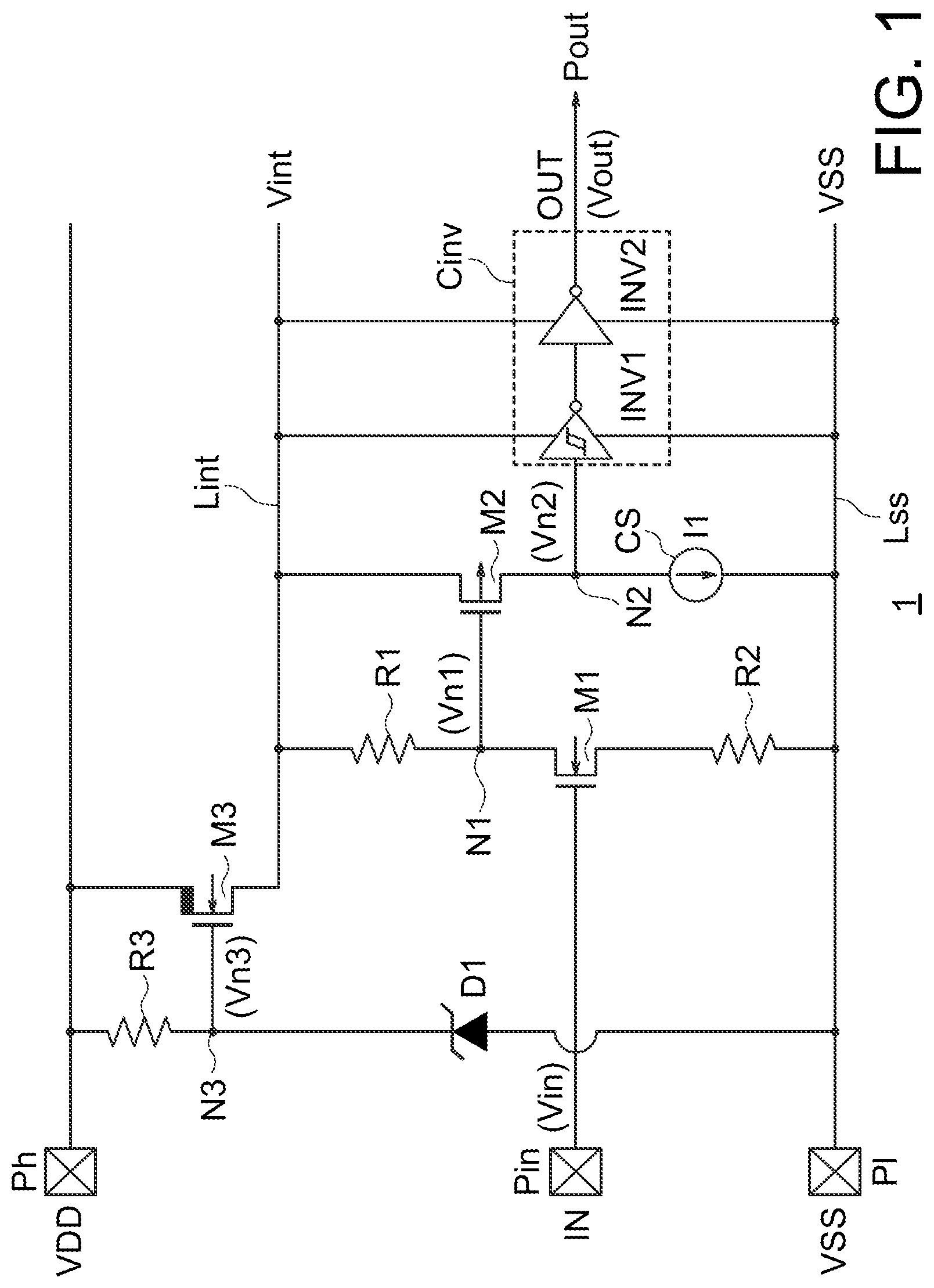
is a circuit diagram illustrating an input circuit 1 of an integrated circuit device according to a first embodiment.
The input circuit 1 includes an input terminal Pin, an output terminal Pout, a first power supply terminal Ph, a second power supply terminal Pl, a first power supply line Lint, a second power supply line Lss, a first transistor M 1 , a second transistor M 2 , a third transistor M 3 , a first resistance element R 1 , a second resistance element R 2 , a third resistance element R 3 , a constant current source CS, an inverter circuit Cinv, and a diode D 1 .
The first power supply terminal Ph receives a high power supply voltage VDD as a first power supply voltage. The second power supply terminal Pl receives a low power supply voltage VSS as a second power supply voltage.
The input terminal Pin receives a control signal from outside. The input voltage of the input terminal Pin is Vin. The output terminal Pout outputs a power supply voltage as any of a predetermined internal power supply voltage Vint or a predetermined power supply voltage VSS based on the control signal from outside received by the input terminal Pin. The output voltage of the output terminal Pout is Vout.
The input circuit 1 outputs an output signal OUT using any of the internal power supply voltage Vint or the power supply voltage VSS based on the logic of an input signal IN input to the input terminal Pin. Accordingly, the input circuit 1 can switch the output voltage Vout between the internal power supply voltage Vint (logical high: ON state) and the power supply voltage VSS (logical low: OFF state) based on the logic of the control signal from the input terminal Pin.
The first transistor M 1 is an n-MOSFET (Metal Oxide Semiconductor Field Effect Transistor), for example. A gate of the first transistor M 1 is connected to the input terminal Pin. A drain of the first transistor M 1 is connected to the first power supply line Lint via the first resistance element R 1 . A source of the first transistor M 1 is connected to the second power supply line Lss via the second resistance element R 2 . Here, “connected” means not only a state of being connected to another part in direct contact, but also a state of being electrically connected to another part via another element.
The first resistance element R 1 is connected between the drain of the first transistor M 1 and the first power supply line Lint.
The second resistance element R 2 is connected between the source of the first transistor M 1 and the second power supply line Lss.
The second transistor M 2 is a p-MOSFET, for example. A gate of the second transistor M 2 is connected to a first node N 1 provided between the drain of the first transistor M 1 and the first resistance element R 1 . The voltage of the first node N 1 is Vn 1 . A source of the second transistor M 2 is connected to the first power supply line Lint. A drain of the second transistor M 2 is connected to the second power supply line Lss via the constant current source CS.
The constant current source CS is connected between the drain of the second transistor M 2 and the second power supply line Lss and functions to pass a constant current I 1 to the second transistor M 2 .
An input part of the inverter circuit Cinv is connected to a second node N 2 provided between the second transistor M 2 and the constant current source CS. An output part of the inverter circuit Cinv is connected to the output terminal Pout.
The inverter circuit Cinv includes a plurality of inverters INV 1 and INV 2 connected in series between the second node N 2 and the output terminal Pout. The input of the former inverter INV 1 is connected to the second node N 2 and the output thereof is connected to the input of the subsequent inverter INV 2 . The voltage of the second node N 2 is Vn 2 . The output of the inverter INV 2 is connected to the output terminal Pout. While the inverter circuit Cinv is constituted by two serially connected inverters, it may be constituted by three or more inverters.
Among the plurality of inverters INV 1 and INV 2 , the former inverter INV 1 connected to the second node N 2 is a Schmitt inverter, for example. Accordingly, the operation of the inverter circuit Cinv can be stable.
Power is respectively fed to the inverters INV 1 and INV 2 between the first power supply line Lint and the second power supply line Lss. Therefore, the inverter INV 1 outputs an inversion signal having a logic according to the voltage level of the second node N 2 as the internal power supply voltage Vint or the second power supply voltage VSS. The inverter INV 2 outputs an inversion signal having a logic according to the voltage level of the output of the inverter INV 1 as the internal power supply voltage Vint or the second power supply voltage VSS.
The third resistance element R 3 and the diode D 1 are connected to each other in series between the first power supply terminal Ph and the second power supply terminal Pl. The diode D 1 is a Zener diode, for example. The anode of the diode D 1 is connected to the second power supply line Lss. The cathode of the diode D 1 is connected to a third node N 3 . The voltage of the third node N 3 is Vn 3 . The diode D 1 is provided to stabilize the voltage of the third node N 3 with respect to voltage fluctuations of the power supply voltages VDD and VSS. The internal power supply voltage Vint is stabilized with respect to voltage fluctuations of the power supply voltages VDD and VSS by stabilizing the voltage of the third node N 3 .
The third transistor M 3 is an n-DMOSFET (Double-Diffused MOSFET), for example. A gate of the third transistor M 3 is connected to the third node N 3 provided between the third resistance element R 3 and the diode D 1 . A drain of the third transistor M 3 is connected to the first power supply terminal Ph. A source of the third transistor M 3 is connected to the first power supply line Lint. By using a DMOSFET as the third transistor M 3 , even when an overvoltage is applied on the first power supply terminal Ph on the drain side, the third transistor M 3 is hardly broken down.
Operations of the input circuit 1 are described next.
A to 2 D are graphs respectively illustrating an operation example of the input circuit 1 according to the first embodiment. The horizontal axis in each of A to 2 D represents the input voltage Vin input from the input terminal Pin. The vertical axis in A represents the output voltage Vout output from the output terminal Pout. The vertical axis in B represents the voltage Vn 1 of the first node N 1 . The vertical axis in C represents the voltage Vn 2 of the second node N 2 . The vertical axis in D represents a current Iinv 1 supplied from the first power supply line Lint to the inverter INV 1 .
With reference to , first, when the high power supply voltage VDD is applied, the gate voltage (Vn 3 ) of the third transistor M 3 is set by the third resistance element R 3 and the diode D 1 . With this setting, the third transistor M 3 is in a conduction state and the internal power supply voltage Vint is on the first power supply line Lint. In this case, even when the high power supply voltage VDD is fluctuated, the third resistance element R 3 and the diode D 1 do not largely fluctuate the voltage Vn 3 and stabilize it. With this configuration, the conduction state of the third transistor M 3 is stabilized and the internal power supply voltage Vint is stabilized with respect to voltage fluctuations of the power supply voltage VDD.
When the input voltage Vin is a low-level voltage (logical low), the first transistor M 1 in is in a non-conduction state. Therefore, the voltage Vn 1 is charged via the first resistance element R 1 and by the internal power supply voltage Vint to be a high-level voltage of the internal power supply voltage Vint. That is, as indicated by the initial values in B , the voltage Vn 1 is a high-level voltage.
Accordingly, the second transistor M 2 in is in a non-conduction state. Therefore, the voltage Vn 2 is decreased by the constant current source CS to be a low-level voltage of the power supply voltage VSS. That is, as indicated by the initial values in C , the voltage Vn 2 is a low-level voltage. In this manner, the second transistor M 2 and the constant current source CS transmit a signal having the same logic as the logic of the input signal IN of the input voltage Vin to the inverter circuit Cinv.
Further, since the input voltage (Vn 2 ) of the inverter circuit Cinv in becomes a low-level voltage, as indicated by the initial values in A , the inverter circuit Cinv outputs a low-level voltage (logical low) as the output voltage Vout. In this manner, when the input signal IN is logical low, the output signal OUT is also outputted as logical low.
Next, a case where the input voltage Vin is switched from a low-level voltage (logical low) to a high-level voltage (logical high) is described.
When the input voltage Vin becomes a high-level voltage (logical high), the first transistor M 1 in is switched from a non-conduction state to a conduction state. Accordingly, the voltage Vn 1 becomes a voltage caused by dividing a voltage difference between the internal power supply voltage Vint and the power supply voltage VSS by the resistance elements R 1 and R 2 (hereinafter, this voltage may be referred to as “voltage-divided value”). Further, the slope of change (voltage response characteristics) in the voltage Vn 1 as it changes from the internal power supply voltage Vint to the voltage-divided value becomes gradual. This slope of change in the voltage Vn 1 is changed with a ratio (R 1 /R 2 ) between the resistance elements R 1 and R 2 .
In A to 2 D , lines L 1 , L 2 , L 3 , L 4 , L 5 , and L 10 represent the output voltage Vout, the voltage Vn 1 of the first node N 1 , the voltage Vn 2 of the second node N 2 , and the current Iinv 1 supplied to the inverter INV 1 when the resistance ratio R 1 /R 2 is 1, 2, 3, 4, 5, and 10, respectively.
For example, as represented with the line L 1 in B , when the resistance ratio R 1 /R 2 is 1, the slope of change in the voltage Vn 1 is small and is very gradual. As the resistance ratio R 1 /R 2 is made larger as it is changed to be 2, 3, 4, and 5, as represented with the lines L 2 , L 3 , L 4 , and L 5 in B , the slope of change in the voltage Vn 1 becomes increasingly larger. As represented with the line L 10 in B , when the resistance ratio R 1 /R 2 is 10, the slope of change in the voltage Vn 1 is relatively steep.
Assuming that the threshold voltage of the second transistor M 2 is Vtm 2 , as illustrated in B , when the voltage Vn 1 is lower than the threshold voltage Vtm 2 , the second transistor M 2 in is switched from a non-conduction state to a conduction state. Any resistance element is not interposed between the first power supply line Lint and the second transistor M 2 and only the constant current I 1 flows from the second node N 2 to the second power supply voltage VSS. Therefore, as the second transistor M 2 enters a conduction state, the second node N 2 is charged from the first power supply line Lint in a short time, and the voltage Vn 2 rises steeply from a low-level voltage to a high-level voltage in a short time as illustrated in C .
In this manner, since the input voltage (Vn 2 ) of the inverter circuit Cinv in becomes a high-level voltage, as illustrated in A , the inverter circuit Cinv switches the output voltage Vout from a low-level voltage (logical low) to a high-level voltage (logical high). When the input signal IN is switched from logical low to logical high in this way, the output signal OUT is also switched from logical low to logical high. With this process, the input circuit 1 can transmit the input signal IN to internal circuits as the output signal OUT of any voltage.
Here, in the input circuit 1 according to the present embodiment, when the input signal IN is switched from logical low to logical high, as illustrated in B , the slope of change in the voltage Vn 1 of the first node N 1 changes according to the resistance ratio R 1 /R 2 and it is gradual.
However, in the present embodiment, the second transistor M 2 and the constant current source CS are interposed between the first transistor M 1 and the inverter circuit Cinv. Therefore, the second transistor M 2 enters a conduction state when the voltage Vn 1 is below the threshold voltage Vtm 2 , and the second transistor M 2 and the constant current source CS cause the voltage Vn 2 of the second node N 2 to rise steeply. As a result, the gradual slope of the voltage Vn 1 illustrated in B becomes a steep slope as that of the voltage Vn 2 illustrated in C . By inputting the voltage Vn 2 with such a steep slope to the inverter circuit Cinv, the flow-through current Iinv 1 in the inverter circuit Cinv is decreased. For example, as illustrated in D , the flow-through current Iinv 1 that flows from the first power supply line Lint to the inverter INV 1 is generated only for a short time at a timing where the second transistor M 2 is switched from a non-conduction state to a conduction state. While the flow-through current Iinv 1 changes to some extent according to the resistance ratio R 1 /R 2 , the change is very small.
Meanwhile, for example, as illustrated in , there is assumed a comparative example where the second transistor M 2 and the constant current source CS illustrated in are omitted and the first node N 1 is connected to the input of the inverter circuit Cinv.
is a circuit diagram illustrating an input circuit according to the comparative example. In this comparative example, the second transistor M 2 and the constant current source CS are omitted. Therefore, the voltage Vn 1 of the first node N 1 illustrated in B is directly input to the inverter circuit Cinv. Here, in order to set the logic of the output signal OUT the same as that of the output signal OUT in , the inverter circuit Cinv is constituted by serially connected three inverters INV 1 to INV 3 .
A to 4 C are graphs respectively illustrating operations of the input circuit according to the comparative example. The horizontal axis in each of A to 4 C represents the input voltage Vin input from the input terminal Pin. The vertical axis in A represents the output voltage Vout. The vertical axis in B represents the voltage Vn 1 of the first node N 1 . The vertical axis in C represents the current Iinv 1 supplied from the first power supply line Lint to the inverter INV 1 . The graph of B may be the same as that of B .
First, the initial state in the comparative example may be the same as that in the first embodiment. Therefore, the first power supply line Lint is charged to the internal power supply voltage Vint.
When the input voltage Vin is a low-level voltage (logical low), the first transistor M 1 in is in a non-conduction state. Therefore, the voltage Vn 1 is charged via the first resistance element R 1 and by the internal power supply voltage Vint to be a high-level voltage of the internal power supply voltage Vint. That is, as indicated by the initial values in B , the voltage Vn 1 is a high-level voltage.
Accordingly, since the input voltage (Vn 1 ) of the inverter circuit Cinv in becomes a high-level voltage, as indicated by the initial values in A , the inverter circuit Cinv outputs a low-level voltage (logical low) as the output voltage Vout. In this manner, when the input signal IN is logical low, the output signal OUT is also outputted as logical low.
Next, a case where the input voltage Vin is switched from a low-level voltage (logical low) to a high-level voltage (logical high) is described.
When the input voltage Vin becomes a high-level voltage (logical high), the first transistor M 1 in is switched from a non-conduction state to a conduction state. Accordingly, the voltage Vn 1 becomes a voltage-divided value caused by dividing a voltage difference between the internal power supply voltage Vint and the power supply voltage VSS by the resistance elements R 1 and R 2 . Further, the slope of change (voltage response characteristics) in the voltage Vn 1 as it changes from the internal power supply voltage Vint to the voltage-divided value becomes gradual. For example, as illustrated in B , while slopes of change are varied according to the resistance ratio R 1 /R 2 with reference to the lines L 1 to L 10 , each slope of change in the voltage Vn 1 is small and gradual.
When the slope of change in the voltage Vn 1 becomes gradual, the slope of change in the input voltage (Vn 1 ) of the inverter circuit Cinv in also becomes gradual. In this case, the voltage range (the range of Vin) of the input signal IN in which the input voltage (Vn 1 ) of the inverter circuit Cinv becomes an intermediate potential is broadened. Accordingly, the flow-through current Iinv 1 flowing in the inverter circuit Cinv is increased as illustrated in C .
For example, as illustrated in B , on the line L 1 , the slope of change in the voltage Vn 1 is very gradual and the inverter INV 1 is not inverted as illustrated in A . In this case, as illustrated in C , the flow-through current Iinv 1 keeps flowing while the input voltage (Vn 1 ) of the inverter circuit Cinv remains to be an intermediate potential. On the lines L 2 to L 10 , while the inverter INV 1 is inverted as illustrated in A , the slope of change in the voltage Vn 1 is still gradual as illustrated in B . In this case, as illustrated in C , the flow-through current Iinv 1 is also relatively large.
Meanwhile, in the present embodiment, as illustrated in , the second transistor M 2 and the constant current source CS are interposed between the first transistor M 1 and the inverter circuit Cinv. With this configuration, as illustrated in C , the second transistor M 2 and the constant current source CS cause the voltage Vn 2 of the second node N 2 to rise steeply. As a result, the gradual slope of the voltage Vn 1 illustrated in B is input to the inverter circuit Cinv as the steep slope of the voltage Vn 2 illustrated in C . Accordingly, as illustrated in D , on each of the lines L 1 to L 10 (in each resistance ratio R 1 /R 2 ), the flow-through current Iinv 1 in the inverter circuit Cinv is decreased. As the flow-through current Iinv 1 is decreased, the entire power consumption of the input circuit 1 can be lowered.
Second Embodiment
is a circuit diagram illustrating the input circuit 1 of an integrated circuit device according to a second embodiment. In the second embodiment, a specific example of internal circuits in the constant current source CS is described.
The constant current source CS includes a fourth resistance element R 4 , a fourth transistor M 4 , and a fifth transistor M 5 .
The fourth resistance element R 4 and the fourth transistor M 4 are connected to each other in series between the first power supply line Lint and the second power supply line Lss. The fourth resistance element R 4 is connected between the first power supply line Lint and a drain and a gate of the fourth transistor M 4 . The fourth transistor M 4 is an n-MOSFET, for example. The drain and the gate of the fourth transistor M 4 are connected to the first power supply line Lint via the fourth resistance element R 4 , and a source of the fourth transistor M 4 is connected to the second power supply line Lss.
A gate of the fifth transistor M 5 is connected to a fourth node N 4 (the gates of the fourth and fifth transistors M 4 and M 5 ) between the fourth transistor M 4 and the fourth resistance element R 4 . A drain of the fifth transistor M 5 is connected to the second node N 2 . A source of the fifth transistor M 5 is connected to the second power supply line Lss.
The fourth and fifth transistors M 4 and M 5 constitute a current mirror circuit. The fourth resistance element R 4 and the fourth transistor M 4 receive the internal power supply voltage Vint from the first power supply line Lint and pass a constant current to the second power supply line Lss. The fifth transistor M 5 that constitutes a current mirror circuit with the fourth transistor M 4 passes a constant current corresponding to the current flowing in the fourth transistor M 4 from the second node N 2 to the second power supply line Lss. In this manner, the constant current source CS is configured to pass the constant current I 1 .
As described above, in the second embodiment, the constant current source CS is configured to pass the constant current I 1 generated by the current mirror circuit (M 4 and M 5 ) based on the current from the first power supply line Lint from the second node N 2 . Even with the configuration in the second embodiment, effects identical to those of the first embodiment can be achieved.
Third Embodiment
is a circuit diagram illustrating the input circuit 1 of an integrated circuit device according to a third embodiment. The input circuit 1 according to the third embodiment further includes a protection circuit CP and a pull-up circuit PU.
The protection circuit CP includes a sixth transistor M 6 . A gate of the sixth transistor M 6 is connected to the third node N 3 with the gate of the third transistor M 3 . A drain of the sixth transistor M 6 is connected to the input terminal Pin. The source of the sixth transistor M 6 is connected to the gate of the first transistor M 1 . Therefore, the sixth transistor M 6 is connected between the input terminal Pin and the gate of the first transistor M 1 . The sixth transistor M 6 is an n-DMOSFET, for example. By using a DMOSFET as the sixth transistor M 6 , even when an overvoltage is applied on the input terminal Pin on the drain side, the sixth transistor M 6 is hardly broken down.
The sixth transistor M 6 receives the voltage Vn 3 of the third node N 3 with the third transistor M 3 . Therefore, when the voltage Vn 3 is caused to rise by the power supply voltage VDD, the sixth transistor M 6 is in a conduction state similarly to the third transistor M 3 .
Assuming that the threshold voltage of the sixth transistor M 6 is Vtm 6 , even when an overvoltage exceeding a voltage Vn 3 -Vtm 6 is applied on the input terminal Pin, the gate-source voltage of the sixth transistor M 6 does not change, and the current flowing between the drain and the source of the sixth transistor M 6 can be suppressed. Accordingly, even when an overvoltage is applied on the input terminal Pin, internal circuits (such as the first transistor M 1 and the pull-up circuit PU) provided in the downstream with respect to the sixth transistor M 6 can be protected.
The pull-up circuit PU includes seventh to ninth transistors M 7 to M 9 . A gate of the seventh transistor M 7 is connected to a drain of the ninth transistor M 9 with a drain and a gate of the eighth transistor M 8 . A source of the seventh transistor M 7 is connected to the first power supply line Lint. A drain of the seventh transistor M 7 is connected to the gate of the first transistor M 1 . That is, the seventh transistor M 7 is connected between the first power supply line Lint and the gate of the first transistor M 1 . The seventh transistor M 7 is a p-MOSFET, for example.
The gate of the eighth transistor M 8 is connected to the drain of the ninth transistor M 9 (the fifth node N 5 ) with the gate of the seventh transistor M 7 and the drain of the eighth transistor M 8 . A source of the eighth transistor M 8 is connected to the first power supply line Lint with the source of the seventh transistor M 7 . The eighth transistor M 8 is a p-MOSFET, for example.
A gate of the ninth transistor M 9 is connected to the gates of the fourth and fifth transistors M 4 and M 5 (the fourth node N 4 ). The drain of the ninth transistor M 9 is connected to the gate of the seventh transistor M 7 and the gate and the drain of the eighth transistor M 8 (the fifth node N 5 ). A source of the ninth transistor M 9 is connected to the second power supply line Lss. Therefore, the ninth transistor M 9 is connected between the fifth node N 5 and the second power supply line Lss. The ninth transistor M 9 is an n-MOSFET, for example.
The ninth transistor M 9 constitutes a current mirror circuit with the fourth and fifth transistors M 4 and M 5 and passes a constant current corresponding to the current flowing in the fourth transistor M 4 from the fifth node N 5 to the second power supply line Lss.
Meanwhile, the seventh and eighth transistors M 7 and M 8 constitute a current mirror circuit. The seventh transistor M 7 passes a constant current corresponding to the current flowing in the eighth transistor M 8 . Accordingly, the seventh transistor M 7 charges the gate of the first transistor M 1 from the first power supply line Lint, thereby pulling up the gate voltage of the first transistor M 1 .
With this configuration, even when the input terminal Pin is open and is not receiving any control signal, the pull-up circuit PU can pull up the gate voltage of the first transistor M 1 to a high-level voltage corresponding to the internal power supply voltage Vint. Accordingly, similarly to a case where the input signal IN is maintaining to be logical high, the first transistor M 1 maintains a conduction state and the output signal OUT maintains to be logical high. As a result, even when the input terminal Pin is open, internal circuits (not illustrated) receiving the output signal OUT can maintain a driving state.
Further, the pull-up circuit PU is constituted by a current mirror circuit formed of the seventh and eighth transistors M 7 and M 8 . Accordingly, a current flowing in the gate of the first transistor M 1 via the seventh transistor M 7 can be suppressed.
For example, if the pull-up circuit PU is constituted by a pull-up resistor (not illustrated) connected between the third node N 3 and the gate of the first transistor M 1 , the resistance value of the pull-up resistor needs to be risen in order to decrease the current flowing from the first power supply line Lint to the gate of the first transistor M 1 . In this case, the element area of the pull-up resistor is inevitably increased.
Meanwhile, in the third embodiment, as long as the size ratio between the seventh and eighth transistors M 7 and M 8 (the mirror ratio of a current mirror circuit) is adjusted, the current flowing from the first power supply line Lint to the gate of the first transistor M 1 can be suppressed without increasing a layout area.
Further, when the pull-up circuit PU is constituted by the pull-up resistor described above, there is a risk that an overvoltage of the input terminal Pin is transmitted to internal circuits via a pull-up resistor element to break down the internal circuits.
Meanwhile, in the third embodiment, the pull-up circuit PU is constituted by the seventh and eighth transistors M 7 and M 8 and the protection circuit CP constituted by the sixth transistor M 6 is provided. Therefore, in the third embodiment, even when an overvoltage is applied to the input terminal Pin, internal circuits can be protected.
The rest of the configuration in the third embodiment may be identical to the corresponding configuration of the first or second embodiment. Therefore, the third embodiment can achieve effects identical to those of the first or second embodiment.
While certain embodiments have been described, these embodiments have been presented by way of example only, and are not intended to limit the scope of the inventions. Indeed, the novel methods and systems described herein may be embodied in a variety of other forms; furthermore, various omissions, substitutions and changes in the form of the methods and systems described herein may be made without departing from the spirit of the inventions. The accompanying claims and their equivalents are intended to cover such forms or modifications as would fall within the scope and spirit of the inventions.
Figures (11)
Citations
This patent cites (9)
- US5438280
- US7683687
- US2019/0109589
- US2021/0203320
- US2002-198795
- US2003-037490
- US4004659
- US2008-211707
- US5567455