Abstract
The disclosure provides a voltage control device for controlling supply voltages of a power amplifier (PA). The voltage control device includes a first processing circuit to provide a first supply voltage to at least one driving stage amplifier of the PA, and a second processing circuit to provide a second supply voltage to an output stage amplifier of the PA. The first supply voltage is generated according to an average-power-tracking (APT) mechanism related to an average power level of a radio frequency (RF) signal transmitted by the PA.
Claims (18)
1. A voltage control device for controlling supply voltages of a power amplifier (PA), the voltage control device comprising: a first processing circuit, configured to provide a first supply voltage to at least one driving stage amplifier of the PA, the first processing circuit comprising: a low dropout (LDO) DC-DC converter, a buck DC-DC converter, a boost DC-DC converter or a buck boost DC-DC converter a second processing circuit, configured to provide a second supply voltage to an output stage amplifier of the PA; wherein the first supply voltage is generated according to an average-power-tracking (APT) mechanism related to an average power level of a radio frequency (RF) signal transmitted by the PA.
10. A power amplifying system, comprising: a power amplifier, comprising: at least one driving stage amplifier; and an output stage amplifier; a first processing circuit, configured to generate a first supply voltage according to an average-power-tracking (APT) mechanism, and provide the first supply voltage to the at least one driving stage amplifier, the first processing circuit comprising: a low dropout (LDO) DC-DC converter, a buck DC-DC converter, a boost DC-DC converter or a buck boost DC-DC converter, a second processing circuit, configured to generate a second supply voltage according to an envelope-tracking-supply-modulation (ETSM) mechanism, and provide the second supply voltage to the output stage amplifier.
Show 16 dependent claims
2. The voltage control device according to claim 1 , wherein the first processing circuit receives a fixed supply voltage from a power source and convert the fixed supply voltage to the first supply voltage according to the APT mechanism.
3. The voltage control device according to claim 1 , wherein the first supply voltage is provided to the at least one driving stage amplifier through a first supply port, the PA has a first equivalent capacitance which is internally parasitic in the PA, and the first equivalent capacitance is related to the first supply port.
4. The voltage control device according to claim 1 , wherein the second supply voltage is generated according to an envelope-tracking-supply-modulation (ETSM) mechanism related to an envelope of the voltage level of the RF signal transmitted by the PA.
5. The voltage control device according to claim 4 , wherein the second processing circuit comprises an analog differential amplifier, and the second supply voltage is an analog modulated supply voltage generated according to the ETSM mechanism.
6. The voltage control device according to claim 4 , wherein the second processing circuit comprises a mixed-signal circuit, and the second supply voltage is a digital modulated supply voltage generated according to the ETSM mechanism.
7. The voltage control device according to claim 1 , wherein the second supply voltage is provided to the output stage amplifier through a second supply port, the PA has a second equivalent capacitance which is internally parasitic in the PA, and the second equivalent capacitance is related to the second supply port.
8. The voltage control device according to claim 7 , wherein the second supply port is further related to a third equivalent capacitance, and the third equivalent capacitance is exterior to the PA.
9. The voltage control device according to claim 8 , wherein a connecting path between the second supply port and the second processing circuit has a fourth equivalent capacitance, and the second supply voltage has a signal bandwidth related to the sum of the second equivalent capacitance, the third equivalent capacitance and the fourth equivalent capacitance.
11. The power amplifying system according to claim 10 , wherein the first supply voltage is related to an average power level of a radio frequency (RF) signal transmitted by the PA.
12. The power amplifying system according to claim 10 , further comprising: a power source, configured to provide a fixed supply voltage to the first processing circuit; wherein the first processing circuit converts the fixed supply voltage to the first supply voltage according to the APT mechanism.
13. The power amplifying system according to claim 10 , further comprising: a first supply port, connected between the first processing circuit and the at least one driving stage amplifier to transmit the first supply voltage; wherein the PA has a first equivalent capacitance which is internally parasitic in the PA, and the first equivalent capacitance is related to the first supply port.
14. The power amplifying system according to claim 10 , wherein the second supply voltage is related to an envelope of the voltage level of the RF signal transmitted by the PA.
15. The power amplifying system according to claim 14 , wherein the second supply voltage is an analog modulated supply voltage or a digital modulated supply voltage generated according to the ETSM mechanism.
16. The power amplifying system according to claim 10 , further comprising: a second supply port, connected between the second processing circuit and the output stage amplifier to transmit the second supply voltage; wherein the PA has a second equivalent capacitance which is internally parasitic in the PA, and the second equivalent capacitance is related to the second supply port.
17. The power amplifying system according to claim 16 , wherein the second supply port is further related to a third equivalent capacitance, and the third equivalent capacitance is exterior to the PA.
18. The power amplifying system according to claim 17 , further comprising: a connecting path, connected between the second supply port and the second processing circuit, the connecting path has a fourth equivalent capacitance; wherein the second supply voltage has a signal bandwidth related to the sum of the second equivalent capacitance, the third equivalent capacitance and the fourth equivalent capacitance.
Full Description
Show full text →
This application claims the benefit of U.S. provisional application Ser. No. 63/178,631, filed Apr. 23, 2021, the subject matter of which is incorporated herein by reference.
TECHNICAL FIELD
The disclosure is relate to a voltage control device, and more particularly, related to a voltage control device for controlling supply voltages of a power amplifier (PA) in a transmitting (TX) front end.
BACKGROUND
As progress of the communication technology, wireless transmission become a must function for a mobile device. Furthermore, to perform wireless transmission, the power amplifier (PA) is a must element for the transmitting (TX) front end. The PA serves to amplify power level of radio frequency (RF) signal to suit the operation condition in wireless environment.
Considering manufacturing factors and element characteristics, parasitic capacitances may appear interior or exterior to the PA. Such parasitic capacitances may seriously degrade signal integrality of the RF signal transmitted by the PA.
To address the aforementioned signal integrality issue of the PA, skilled ones in this technical field are devoted to improve configuration and operating mechanism for the PA, in order to achieve better signal integrality for the RF signal.
SUMMARY
According to one aspect of the present disclosure, a voltage control device is provided. The voltage control device controls supply voltages of a power amplifier (PA). The voltage control device includes a first processing circuit to provide a first supply voltage to at least one driving stage amplifier of the PA, and a second processing circuit to provide a second supply voltage to an output stage amplifier of the PA. The first supply voltage is generated according to an average-power-tracking (APT) mechanism related to an average power level of a radio frequency (RF) signal transmitted by the PA.
According to another aspect of the present disclosure, a power amplifying system is provided. The power amplifying system includes a power amplifier having at least one driving stage amplifier and an output stage amplifier, a first processing circuit to generate a first supply voltage according to an average-power-tracking (APT) mechanism and provide the first supply voltage to the at least one driving stage amplifier, and a second processing circuit to generate a second supply voltage according to an envelope-tracking-supply-modulation (ETSM) mechanism and provide the second supply voltage to the output stage amplifier.
BRIEF DESCRIPTION OF THE DRAWINGS
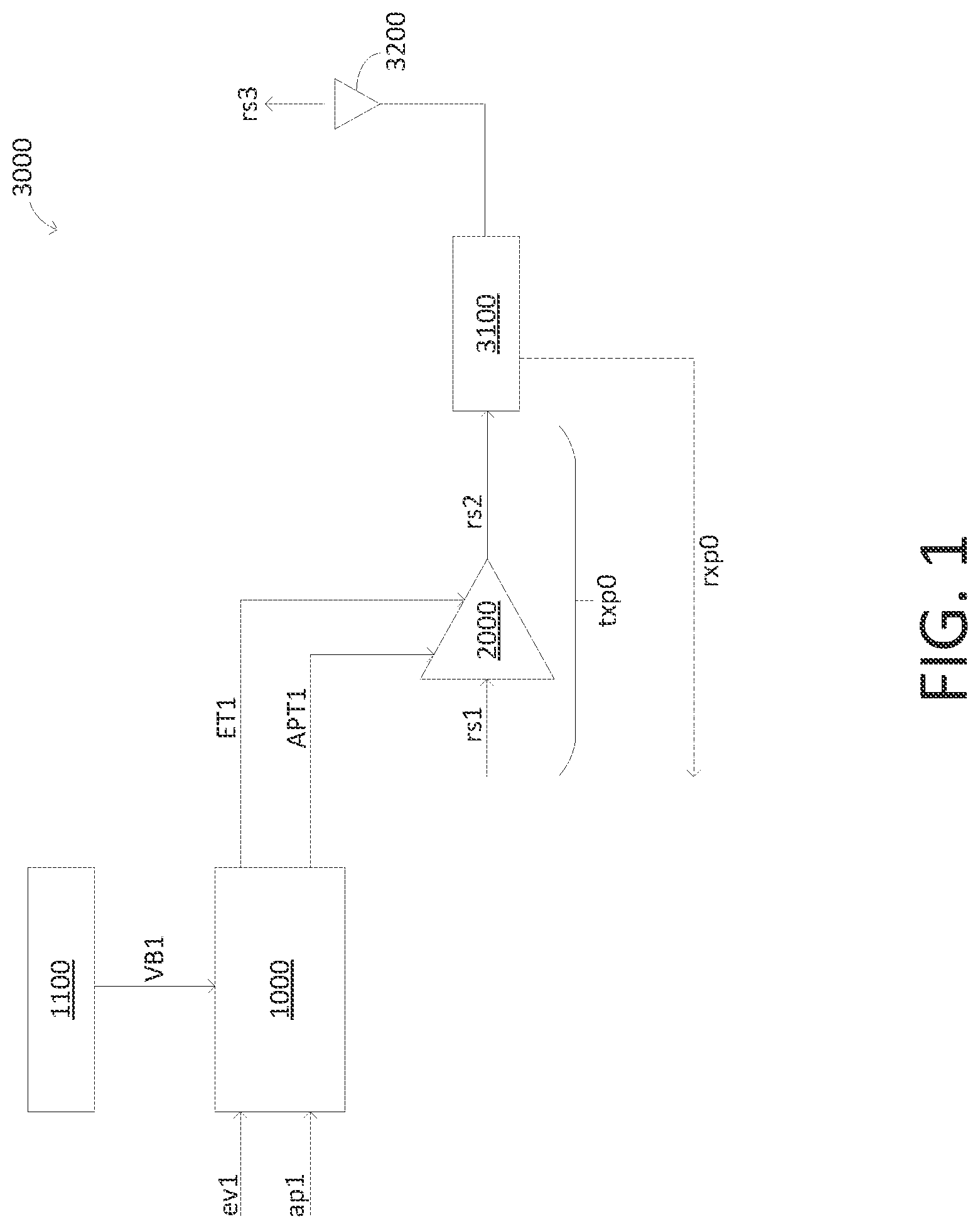
is a schematic block diagram of a transmitting (TX) front end 3000 which includes a voltage control device 1000 of an example of the present disclosure.
A is a diagram of voltage level of the RF signal versus time.
B is a diagram of voltage level of the supply voltage versus time.
A is another diagram of voltage level of the RF signal versus time.
B is a diagram of voltage level of the supply voltage versus time.
is a schematic block diagram illustrating the voltage control device and the PA of an example of the present disclosure.
is a schematic block diagram illustrating a voltage control device and a PA of a TX front end in a comparative example.
is a schematic block diagram of one example of the voltage control device of .
A is a schematic block diagram illustrating another example of voltage control device and the PA of the present disclosure.
B is a schematic block diagram of the processing circuit of A .
In the following detailed description, for purposes of explanation, numerous specific details are set forth in order to provide a thorough understanding of the disclosed embodiments. It will be apparent, however, that one or more embodiments may be practiced without these specific details. In other instances, well-known structures and devices are schematically illustrated in order to simplify the drawing.
DETAILED DESCRIPTION
is a schematic block diagram of a transmitting (TX) front end 3000 which includes a voltage control device 1000 of an example of the present disclosure. Referring to , the TX front end 3000 includes a power source 1100 , a voltage control device 1000 , a power amplifier (PA) 2000 , a switch circuit 3100 and an antenna 3200 . The TX front end 3000 functions to transmit radio frequency (RF) signal for an electronic device in a wireless manner.
The PA 2000 receives a modulated RF signal rs 1 from a modulator (not shown in ), and the RF signal rs 1 has a desired operating frequency suitable for wireless transmission. The PA 2000 serves to amplify the power level of the RF signal rs 1 , obtaining a RF signal rs 2 with desired power level suitable for operating condition of the electronic device. The switch circuit 3100 serves to selectively couple the TX path txp 0 or the receiving (RX) path rxp 0 to the antenna 3200 . When the electronic device operates to transmit, the RF signal rs 2 is transmitted to the antenna 3200 through the TX path txp 0 and the switch circuit 3100 . The antenna 3200 serves to generate a radiation signal rs 3 according to the RF signal rs 2 .
The PA 2000 operates with at least two DC supply voltages: a supply voltage APT 1 and a supply voltage ET 1 , in which the PA 2000 is powered according to the supply voltages APT 1 and ET 1 . The voltage levels of the supply voltages APT 1 and ET 1 are not fixed, but can be dynamically adjusted according to current condition the electronic device operates. For an operating condition the RF signal rs 2 needs to be amplified as a greater power level, the supply voltages APT 1 and ET 1 may be adjusted as a greater voltage level, otherwise, voltage level of the supply voltages APT 1 and ET 1 may be lowered.
The voltage control device 1000 serves to provide the supply voltages APT 1 and ET 1 and adjust voltage levels thereof. The power source 1100 serves to provide a supply voltage VB 1 to the voltage control device 1000 . The supply voltage VB 1 is a fixed supply voltage with a fixed voltage level. In one example, the power source 1100 refers to a battery, and the supply voltage VB 1 is a fixed battery voltage of 1.5 volts.
More particularly, the supply voltage APT 1 may be referred to as “the first supply voltage”, and the voltage control device 1000 may control the supply voltage APT 1 according to an “average-power-tracking (APT)” mechanism. Furthermore, the supply voltage ET 1 may be referred to as “the second supply voltage”, which may be controlled according to an “envelope-tracking-supply-modulating (ETSM)” mechanism.
A is a diagram of voltage level of the RF signal rs 2 versus time, and B is a diagram of voltage level of the supply voltage APT 1 versus time, both of which illustrate the APT mechanism performed to the supply voltage APT 1 . Referring to A , the average power level 20 of the RF signal rs 2 may be measured, and a control signal ap 1 related to the average power level 20 may be obtained. The voltage control device 1000 may be configured to adjust the supply voltage APT 1 according to the control signal ap 1 . When the average power level 20 of the RF signal rs 2 decreases, indicating that the PA 2000 requires less supply power, hence the voltage control device 1000 lowers voltage level of the supply voltage APT 1 , as shown in B . Compared with a fixed supply voltage VCC 0 , the supply voltage APT 1 may be dynamically adjusted according to the average power level 20 of the RF signal rs 2 , so that power dissipation by the PA 2000 may be reduced.
On the other hand, with the ETSM mechanism, the supply voltage ET 1 is “constantly” (i.e., more frequently and precisely) adjusted according to the envelope of the RF signal rs 2 , thus the PA 2000 may further reduce its power dissipation. A is another diagram of voltage level of the RF signal rs 2 versus time, and B is a diagram of voltage level of the supply voltage ET 1 versus time, both of which illustrate the ETSM mechanism performed to the supply voltage ET 1 . Referring to A , envelope 30 of the RF signal rs 2 may be measured, and a control signal ev 1 related to the envelope 30 is obtained. According to the control signal ev 1 , the voltage control device 1000 may be configured to “constantly” adjust the supply voltage ET 1 as shown in B . In the ETSM mechanism, voltage level of the RF signal rs 2 may be tracked more precisely, hence the supply voltage ET 1 may be immediately adjusted to further reduce power dissipation of the PA 2000 .
In the example of , the average power level 20 and envelope 30 of the RF signal rs 2 are measured by a separated element (not shown in ) other than the voltage control device 1000 , and the control signals ap 1 and ev 1 may be generated in such a separated element. In other examples (not shown in ), the voltage control device 1000 may serve to measure the average power level 20 and envelope 30 of the RF signal rs 2 , and the control signals ap 1 and ev 1 may be internally generated by the voltage control device 1000 .
The supply voltage ET 1 may be of analog type or digital type. In one example, the supply voltage ET 1 is an analog modulated supply voltage referred to as “supply voltage AET 1 ”. In another example, the supply voltage ET 1 is a digital modulated supply voltage referred to as “supply voltage DET 1 ”.
is a schematic block diagram illustrating the voltage control device 1000 and the PA 2000 of an example of the present disclosure. In the example of , the voltage control device 1000 provides a supply voltage AET 1 which is an analog modulated supply voltage. Referring to , the voltage control device 1000 includes a processing circuit 100 and a processing circuit 200 . The processing circuit 100 , which may be referred to as “the first processing circuit”, serves to provide the supply voltage APT 1 according to the control signal ap 1 and the supply voltage VB 1 . In one example, the processing circuit 100 may include a DC-DC converter. The DC-DC converter may be a low dropout (LDO) DC-DC converter, a buck DC-DC converter, a boost DC-DC converter or a buck boost DC-DC converter. The DC-DC converter functions to convert the supply voltage VB 1 to the supply voltage APT 1 and adjust voltage level of the supply voltage APT 1 based on the control signal ap 1 .
The processing circuit 200 , which may be referred to as “the second processing circuit”, serves to provide the supply voltage AET 1 according to the control signal ev 1 and the supply voltage VB 1 . Similar to the processing circuit 100 , the processing circuit 200 may also include a DC-DC converter functioning to convert the supply voltage VB 1 to the supply voltage AET 1 . The DC-DC converter of the processing circuit 200 may be a LDO DC-DC converter, a buck DC-DC converter, a boost DC-DC converter or a buck boost DC-DC converter. Furthermore, the processing circuit 200 adjusts the supply voltage AET 1 according to the control signal ev 1 with the ETSM mechanism.
The PA 2000 includes a driving stage 700 and an output stage 800 . The driving stage 700 includes at least one amplifier, e.g., the driving stage amplifier 700 - 1 to 700 - n . The driving stage amplifiers 700 - 1 to 700 - n are coupled to a supply port Vcc 1 , and the supply port Vcc 1 is coupled to the processing circuit 100 to receive the supply voltage APT 1 . The PA 2000 may have an internally parasitic capacitance C 1 , which may be measured on a connecting path P 1 between the supply port Vcc 1 and the driving stage amplifiers 700 - 1 to 700 - n . The supply port Vcc 1 may be referred to as “the first supply port”, and the capacitance C 1 may be referred to as “the first equivalent capacitance”, and the capacitance C 1 is related to the supply port Vcc 1 .
The output stage 800 includes an output stage amplifier 800 - 1 . The output stage amplifier 800 - 1 receives the supply voltage AET 1 through a supply port Vcc 2 . The supply port Vcc 2 , which may be referred to as “the second supply port”, is coupled to the processing circuit 200 to receive the supply voltage AET 1 . Another capacitance C 2 internally parasitic in the PA 2000 may be measured on a connecting path P 2 between the supply port Vcc 2 and the output stage amplifiers 800 - 1 . The capacitance C 2 , which may be referred to as “the second equivalent capacitance”, is related to the supply port Vcc 2 .
Furthermore, an external parasitic capacitance C 3 which is exterior to the PA 2000 , may be measured on a connecting path P 3 between the supply port Vcc 2 and the processing circuit 200 . The capacitance C 3 may be identified at a location exterior to the PA 2000 and near the supply port Vcc 2 . The capacitance C 3 is also related to the supply port Vcc 2 and may be referred to as “the third equivalent capacitance”.
Moreover, a capacitance C 4 and an inductance L 1 may be also measured on the connecting path P 3 between the supply port Vcc 2 and the processing circuit 200 . The capacitance C 4 and the inductance L 1 are related to a routing wire of a circuit board which forms the connecting path P 3 between the supply port Vcc 2 and the processing circuit 200 . The capacitance C 4 may be referred to as the “fourth equivalent capacitance”.
Base on the aforementioned configuration of the voltage control device 1000 and the PA 2000 , the capacitances C 2 , C 3 and C 4 are formed in a parallel manner with respect to the connecting paths P 3 and P 2 . Hence, when observing from the processing circuit 200 to the output stage amplifier 800 - 1 through the connecting paths P 3 , the supply port Vcc 2 and the connecting path P 2 , an total equivalent capacitance Ct may be obtained as a sum of the capacitances C 2 , C 3 and C 4 as equation (1): Ct=C 2+ C 3+ C 4 eq. (1)
Furthermore, the supply voltage AET 1 has a signal bandwidth BW 1 related to total equivalent capacitance Ct. The smaller value of the total equivalent capacitance Ct may result in greater signal bandwidth BW 1 for the supply voltage AET 1 . With the greater signal bandwidth BW 1 , the PA 2000 may achieve better linearity and suffer less distortion, and the RF signal rs 2 may hence achieve better signal integrity.
is a schematic block diagram illustrating a voltage control device 1000 b and a PA 2000 b of a TX front end 3000 b in a comparative example. Referring to , the voltage control device 1000 b merely provides one supply voltage ET 1 b to the PA 2000 b . The driving stage amplifiers 700 - 1 to 700 - n receives the supply voltage ET 1 b through the supply port Vcc 1 , and the output stage amplifier 800 - 1 receives the supply voltage ET 1 b through the supply port Vcc 2 . Capacitances C 1 and C 5 related to the supply port Vcc 1 may be measured, where the capacitance C 1 is internally parasitic to the PA 2000 b and the capacitance C 5 is exterior to the PA 2000 b . Likewise, capacitances C 3 and C 2 related to the supply port Vcc 2 may be measured, where the capacitance C 2 is internally parasitic to the PA 2000 b and the capacitance C 3 is exterior to the PA 2000 b . Furthermore, the capacitance C 4 may be measured on the routing wire of the circuit board forming the connecting path P 3 . Since the supply voltage ET 1 b is provided to the driving stage amplifiers 700 - 1 to 700 - n and the output stage amplifier 800 - 1 through the supply ports Vcc 1 and Vcc 2 , the total equivalent capacitance Ctb related to the supply voltage ET 1 b may be obtained as a sum of the capacitances C 1 , C 5 , C 2 , C 3 and C 4 as equation (2): Ct=C 1+ C 5+ C 2+ C 3+ C 4 eq. (2)
Compared with the total equivalent capacitance Ctb of the comparative example of , the voltage control device 1000 of the present disclosure shown in may provide smaller value of total equivalent capacitance Ct. Hence, the voltage control device 1000 of may achieve wider signal bandwidth BW 1 for the supply voltage AET 1 .
is a schematic block diagram of one example of the voltage control device 1000 of . Referring to , the processing circuit 200 (i.e., the second processing circuit) of the voltage control device 1000 may include a converter 210 , an amplifier 220 and a feedback circuit 230 . The converter 210 may be a DC-DC converter (e.g., a LDO DC-DC converter, a buck DC-DC converter, a boost DC-DC converter or a buck boost DC-DC converter) serving to convert the supply voltage VB 1 to the supply voltage AET 1 . The amplifier 220 , which is an analog differential amplifier (e.g., an “OP Amp”), may function as an error amplifier to provide an error current I_err to the converter 210 . The error current I_err is generated based on the control signal ev 1 and a feedback signal fb 1 , and the feedback circuit 230 serves to provide the feedback signal fb 1 based on the supply voltage AET 1 . When the voltage level of the supply voltage AET 1 departs from the control signal ev 1 (i.e., the voltage level of the supply voltage AET 1 departs from the envelope 30 of the RF signal rs 2 ), the error current I_err may have a larger current value, and the converter 210 may sink or source a control current I_sv to adjust voltage level of the supply voltage AET 1 .
The processing circuit 100 (i.e., the first processing circuit) of the voltage control device 1000 may include a converter 110 . Similar to the converter 210 of the processing circuit 200 , the converter 110 may also be a DC-DC converter (e.g., a LDO DC-DC converter, a buck DC-DC converter, a boost DC-DC converter or a buck boost DC-DC converter) serving to convert the supply voltage VB 1 to the supply voltage APT 1 . Furthermore, the converter 110 is configured to adjust the supply voltage APT 1 based on the control signal ap 1 , so that the voltage level of the supply voltage APT 1 may approximately fit the average power level 20 of the RF signal rs 2 .
A is a schematic block diagram illustrating another example of voltage control device 1000 c and the PA 2000 of the present disclosure. Referring to A , the voltage control device 1000 c is similar to the voltage control device 1000 of except that, the voltage control device 1000 c provides a supply voltage DET 1 of digital type. The processing circuit 200 c of the voltage control device 1000 c may have a circuit capable of processing mixed signal, so that the supply voltage DET 1 may be generated as a digital modulated supply voltage according to the ETSM mechanism.
B is a schematic block diagram of the processing circuit 200 c of A . Referring to A , the processing circuit 200 c is similar to the processing circuit 200 of except that, the amplifier 220 (i.e., an analog differential amplifier) of may be replaced by a mixed-signal circuit 220 c . The mixed-signal circuit 220 c serves to estimate an error value between the control signal ev 1 and the supply voltage DET 1 . With aid of the error value, the converter 210 c may adjust the supply voltage DET 1 as a desired voltage level to fit the envelope 30 of the RF signal rs 2 , and ETSM mechanism is achieved.
It will be apparent to those skilled in the art that various modifications and variations can be made to the disclosed embodiments. It is intended that the specification and examples be considered as exemplary only, with a true scope of the disclosure being indicated by the following claims and their equivalents.
Figures (10)
Citations
This patent cites (5)
- US9263991
- US10153741
- US10784820
- US2014/0273897
- US2022/0311388