Electrostatic Discharge Circuit and Method of Operating Same
Abstract
An electrostatic discharge (ESD) circuit includes a first ESD detection circuit, a first discharging circuit and a first ESD assist circuit. The first ESD detection circuit is coupled between a first node having a first voltage and a second node having a second voltage. The first discharging circuit includes a first transistor. The first transistor has a first gate, a first drain, a first source and a first body terminal. The first gate is coupled to the first ESD detection circuit by a third node. The first drain is coupled to the first node. The first source and the first body terminal are coupled together at the second node. The first ESD assist circuit is coupled between the second and third node, and configured to clamp a third voltage of the third node at the second voltage during an ESD event at the first or second node.
Claims (20)
1. An electrostatic discharge (ESD) circuit comprising: a first ESD detection circuit coupled between a first node and a second node, the first node having a first voltage and the second node having a second voltage; a first discharging circuit comprising a first transistor of a first type, the first transistor having a first gate, a first drain, a first source and a first body terminal, the first gate is coupled to at least the first ESD detection circuit by a third node, the first drain is coupled to the first node, and the first source and the first body terminal are coupled together at the second node; a first ESD assist circuit coupled between the second node and the third node, and configured to clamp a third voltage of the third node at the second voltage during an ESD event at the first node or the second node; a second ESD detection circuit coupled between the second node and a fourth node; a second clamp circuit comprising a second transistor of the first type, the second transistor having a second gate, a second drain, a second source, and a second body terminal, the second gate coupled to at least the second ESD detection circuit by a fifth node, the second drain coupled to the second node, and the second source and the second body terminal coupled together at the fourth node; and a second ESD assist circuit coupled between the fourth node and the fifth node, and configured to clamp a fourth voltage of the fifth node at the second voltage during an ESD event at the second node or the fourth node.
11. An electrostatic discharge (ESD) circuit comprising: a first diode coupled between a first node and an input output (IO) pad; a second diode coupled between the IO pad and a second node; an internal circuit coupled to the first diode, the second diode and the IO pad; and an ESD discharging circuit between the first node and the second node, the ESD discharging circuit comprising: a first ESD detection circuit coupled between the first node and a third node, the first node having a first voltage and the third node having a second voltage; a first clamp circuit comprising a first transistor of a first type, the first transistor having a first gate, a first drain, a first source and a first body terminal, the first gate being coupled to at least the first ESD detection circuit by a fourth node, the first drain being coupled to the first node, and the first source and the first body terminal coupled together at the third node; a first ESD assist circuit coupled between the third node and the fourth node, and configured to clamp a third voltage of the fourth node at the first voltage during an ESD event at the first node or the second node; a second ESD detection circuit coupled between the second node and the third node; a second clamp circuit comprising a second transistor of the first type, the second transistor having a second gate, a second drain, a second source, and a second body terminal, the second gate coupled to at least the second ESD detection circuit by a fifth node, the second drain coupled to the third node, and the second source and the second body terminal coupled together at the second node; and a second ESD assist circuit coupled between the second node and the fifth node, and configured to clamp a fourth voltage of the fifth node at the second voltage during an ESD event at the third node.
20. A method of operating an electrostatic discharge (ESD) circuit, the method comprising: receiving a first ESD voltage on a first node, the first ESD voltage being greater than a reference supply voltage of a reference voltage supply, the first ESD voltage corresponding to a first ESD event; detecting, by a detection circuit, the first ESD event at the first node thereby causing the detection circuit to charge a first gate of a first transistor of a first clamp circuit; turning on a first ESD assist circuit in response to the first ESD event at the first node thereby causing the first ESD assist circuit to clamp a first voltage of the first gate of the first transistor of the first clamp circuit at a second voltage of a second node, the first clamp circuit being coupled between the first node and the second node, and the first ESD assist circuit being coupled between at least the first node and a third node, and the first ESD assist circuit including a first body diode; turning on the first clamp circuit in response to the first ESD event and the first ESD assist circuit clamping the first voltage of the first gate at the second voltage; discharging a first ESD current of the first ESD event in a first ESD direction from the first node to the second node by the first transistor; turning on a second ESD assist circuit in response to the first ESD current of the first ESD event at the second node thereby causing the second ESD assist circuit to clamp a third voltage of a second gate of a second transistor of a second clamp circuit at a fourth voltage of a fourth node, the second clamp circuit being coupled between the second node and the fourth node, and the second ESD assist circuit being coupled between at least the fourth node and a fifth node, and the second ESD assist circuit including a second body diode; turning on the second clamp circuit in response to the first ESD current at the second node and the second ESD assist circuit clamping the third voltage of the second gate at the fourth voltage; and discharging the first ESD current of the first ESD event in the first ESD direction from the second node to the fourth node by the second transistor.
Show 17 dependent claims
2. The ESD circuit of claim 1 , further comprising: a first conductive line extending in a first direction, and configured to supply the first voltage; a second conductive line extending in the first direction, and configured to supply the second voltage; a third conductive line extending in the first direction, and the third conductive line including the third node; a fourth conductive line extending in the first direction, and configured to supply the first voltage; and a fifth conductive line extending in the first direction, and configured to supply the second voltage.
3. The ESD circuit of claim 2 , wherein the first node is part of the first conductive line or the fourth conductive line; the second node is part of the second conductive line or the fifth conductive line; each of the first conductive line, the second conductive line, the third conductive line, the fourth conductive line and the fifth conductive line are separated from each other in a second direction different from the first direction; the third conductive line is between the first conductive line and the fourth conductive line; the first conductive line is between the third conductive line and the second conductive line; and the fourth conductive line is between the third conductive line and the fifth conductive line.
4. The ESD circuit of claim 1 , wherein the first ESD assist circuit comprises: a diode coupled between the second node and the third node, the diode having an anode coupled to the third node, the first gate and the first ESD detection circuit, and a cathode coupled to the second node, the first source and the first body terminal.
5. The ESD circuit of claim 1 , wherein the first ESD assist circuit comprises: a third transistor of the first type, and having a third gate, a third drain, a third source, and a third body terminal, the third drain being coupled to the third node, the first gate and the first ESD detection circuit, and each of the second node, the first source, the first body terminal, the third gate, the third source and the third body terminal being coupled together.
6. The ESD circuit of claim 5 , wherein the third transistor comprises: a first active region in a substrate, the first active region corresponding to the third drain of the third transistor; a second active region in the substrate, the second active region corresponding to the third source of the third transistor; and a third active region in the substrate, the third active region corresponding to the third body terminal of the third transistor, wherein the second active region and the third active region are coupled together, and the first active region and the third active region are configured as a body diode of the third transistor.
7. The ESD circuit of claim 1 , wherein the first ESD assist circuit comprises: a first bipolar junction transistor having a first base, a first collector and a first emitter, the first collector being coupled to the third node, the first gate and the first ESD detection circuit, and each of the first node, the first base, the first emitter, the first source, and the first body terminal being coupled together.
8. The ESD circuit of claim 1 , wherein the first ESD assist circuit comprises: a third transistor of a second type different from the first type, and having a third gate, a third drain, a third source, and a third body terminal, the third drain being coupled to the second node, and each of the third gate, the third source, the third body terminal, the third node, the first gate and the first ESD detection circuit being coupled together.
9. The ESD circuit of claim 8 , wherein the third transistor comprises: a first active region in a substrate, the first active region corresponding to the third drain of the third transistor; a second active region in the substrate, the second active region corresponding to the third source of the third transistor; and a third active region in the substrate, the third active region corresponding to the third body terminal of the third transistor, wherein the second active region and the third active region are coupled together, and the first active region and the third active region are configured as a body diode of the third transistor.
10. The ESD circuit of claim 1 , wherein the first ESD assist circuit comprises: a first bipolar junction transistor having a first base, a first collector and a first emitter, the first collector being coupled to the second node, the first source and the first body terminal, and each of the first emitter, the first base, the third node, the first gate and the first ESD detection circuit being coupled together.
12. The ESD circuit of claim 11 , wherein the first ESD detection circuit comprises: a first resistor coupled between the first node and a first input node; a first capacitor coupled between the first input node and the third node; and a first inverter coupled to the first node, the fourth node, the third node, the first input node, the first gate and the first ESD assist circuit.
13. The ESD circuit of claim 12 , wherein the first inverter comprises: a third transistor of the first type, the third transistor having a third gate, a third drain, a third source, and a third body terminal; and a fourth transistor of a second type different from the first type, the fourth transistor having a fourth gate, a fourth drain, a fourth source, and a fourth body terminal; wherein each of the third gate, the fourth gate, and the first input node are coupled together; each of the third source, the third body terminal, the third node, the first source and the first body terminal are coupled together; each of the fourth source, the fourth body terminal, the first node, and the first drain are coupled together; and each of the third drain, the fourth drain, the first gate and the third node are coupled together.
14. The ESD circuit of claim 13 , wherein the second ESD detection circuit comprises: a second resistor coupled between the third node and a second input node; a second capacitor coupled between the second input node and the second node; and a second inverter coupled to the second node, the third node, the fifth node, the second input node, the second gate and the second ESD assist circuit.
15. The ESD circuit of claim 14 , wherein the second inverter comprises: a fifth transistor of the first type, the fifth transistor having a fifth gate, a fifth drain, a fifth source, and a fifth body terminal; and a sixth transistor of the second type, the sixth transistor having a sixth gate, a sixth drain, a sixth source, and a sixth body terminal; wherein each of the fifth gate, the sixth gate, and the second input node are coupled together; each of the fifth source, the fifth body terminal, the second node, the second source and the second body terminal are coupled together; each of the sixth source, the sixth body terminal, the third node, and the second drain are coupled together; and each of the fifth drain, the sixth drain, the second gate and the fifth node are coupled together.
16. The ESD circuit of claim 11 , wherein the first ESD assist circuit comprises: a third transistor of the first type, and having a third gate, a third drain, a third source, and a third body terminal, the third drain being coupled to the fourth node, the first gate and the first ESD detection circuit, and each of the third node, the first source, the first body terminal, the third gate, the third source and the third body terminal being coupled together.
17. The ESD circuit of claim 11 , wherein the first ESD assist circuit comprises: a first bipolar junction transistor having a first base, a first collector and a first emitter, the first collector being coupled to the fourth node, the first gate and the first ESD detection circuit, and each of the third node, the first base, the first emitter, the first source, and the first body terminal being coupled together.
18. The ESD circuit of claim 11 , wherein the first ESD assist circuit comprises: a diode coupled between the fourth node and the third node, the diode having an anode coupled to the fourth node, the first gate and the first ESD detection circuit, and a cathode coupled to the third node, the first source and the first body terminal.
19. The ESD circuit of claim 11 , further comprising: a first conductive line extending in a first direction, and configured to supply the first voltage; a second conductive line extending in the first direction, and configured to supply the second voltage; a third conductive line extending in the first direction, and the third conductive line including the third node; a fourth conductive line extending in the first direction, and configured to supply the first voltage; and a fifth conductive line extending in the first direction, and configured to supply the second voltage.
Full Description
Show full text →
PRIORITY CLAIM
The present application is a continuation of U.S. application Ser. No. 17/452,281, filed Oct. 26, 2021, now U.S. Pat. No. 11,848,554, issued Dec. 19, 2023, which claims the benefit of U.S. Provisional Application No. 63/177,629, filed Apr. 21, 2021, which are herein incorporated by reference in their entireties.
BACKGROUND
The recent trend in miniaturizing integrated circuits (ICs) has resulted in smaller devices which consume less power, yet provide more functionality at higher speeds than before. The miniaturization process has also increased the devices' susceptibility to electrostatic discharge (ESD) events due to various factors, such as thinner dielectric thicknesses and associated lowered dielectric breakdown voltages. ESD is one of the causes of electronic circuit damage and is also one of the considerations in semiconductor advanced technology.
BRIEF DESCRIPTION OF THE DRAWINGS
Aspects of the present disclosure are best understood from the following detailed description when read with the accompanying FIGURES. It is noted that, in accordance with the standard practice in the industry, various features are not drawn to scale. In fact, the dimensions of the various features may be arbitrarily increased or reduced for clarity of discussion.
is a schematic block diagram of an integrated circuit, in accordance with some embodiments.
A- 2 E are corresponding circuit diagrams of corresponding integrated circuits, in accordance with some embodiments.
A- 3 E are corresponding cross-sectional views of corresponding integrated circuits, in accordance with some embodiments.
A- 4 E are corresponding circuit diagrams of corresponding integrated circuits, in accordance with some embodiments.
A- 5 E are corresponding cross-sectional views of corresponding integrated circuits, in accordance with some embodiments.
A- 6 B are corresponding circuit diagrams of corresponding integrated circuits, in accordance with some embodiments.
A- 7 B are corresponding circuit diagrams of corresponding integrated circuits, in accordance with some embodiments.
A- 8 B are top-views of corresponding integrated circuits, in accordance with some embodiments.
is a flowchart of a method of operating an ESD circuit, in accordance with some embodiments.
is a flow chart of a method of manufacturing an integrated circuit, in accordance with some embodiments.
DETAILED DESCRIPTION
The following disclosure provides different embodiments, or examples, for implementing features of the provided subject matter. Specific examples of components, materials, values, steps, arrangements, or the like, are described below to simplify the present disclosure. These are, of course, merely examples and are not limiting. Other components, materials, values, steps, arrangements, or the like, are contemplated. For example, the formation of a first feature over or on a second feature in the description that follows may include embodiments in which the first and second features are formed in direct contact, and may also include embodiments in which additional features may be formed between the first and second features, such that the first and second features may not be in direct contact. In addition, the present disclosure may repeat reference numerals and/or letters in the various examples. This repetition is for the purpose of simplicity and clarity and does not in itself dictate a relationship between the various embodiments and/or configurations discussed.
Further, spatially relative terms, such as “beneath,” “below,” “lower,” “above,” “upper” and the like, may be used herein for ease of description to describe one element or feature's relationship to another element(s) or feature(s) as illustrated in the FIGURES. The spatially relative terms are intended to encompass different orientations of the device in use or operation in addition to the orientation depicted in the FIGURES. The apparatus may be otherwise oriented (rotated 90 degrees or at other orientations) and the spatially relative descriptors used herein may likewise be interpreted accordingly.
In some embodiments, an electrostatic discharge (ESD) circuit includes an ESD detection circuit coupled between a first node and a second node. In some embodiments, the first node has a first voltage, and the second node has a second voltage.
In some embodiments, the ESD circuit further includes a clamp circuit that includes a first transistor of a first type. The first transistor has a first gate, a first drain, a first source and a first body terminal. The first gate is coupled to at least the ESD detection circuit by a third node. The first drain is coupled to the second node. The first source and the first body terminal are coupled together at the first node.
The ESD circuit further includes an ESD assist circuit that is coupled between the first node and the third node. During an ESD event at the first node or the second node of the present disclosure, the ESD assist circuit is configured to clamp a third voltage of the third node at the first voltage thereby controlling a gate potential of the first transistor and causing the first transistor to turn-on. In response to turning on, the first transistor is configured to discharge an ESD current of the ESD event in a forward ESD direction from the second node to the first node, in accordance with some embodiments.
In some embodiments, by including the ESD assist circuit in the integrated circuit of the present disclosure, the ESD assist circuit is configured to reduce capacitive coupling effects between the first node and the second node and effectively lowers the turn-on resistance of the first transistor. In some embodiments, by lowering the turn-on resistance of the first transistor causing the first transistor to turn-on faster and stronger than other approaches results in improved ESD performance and improved ESD robustness compared to other approaches.
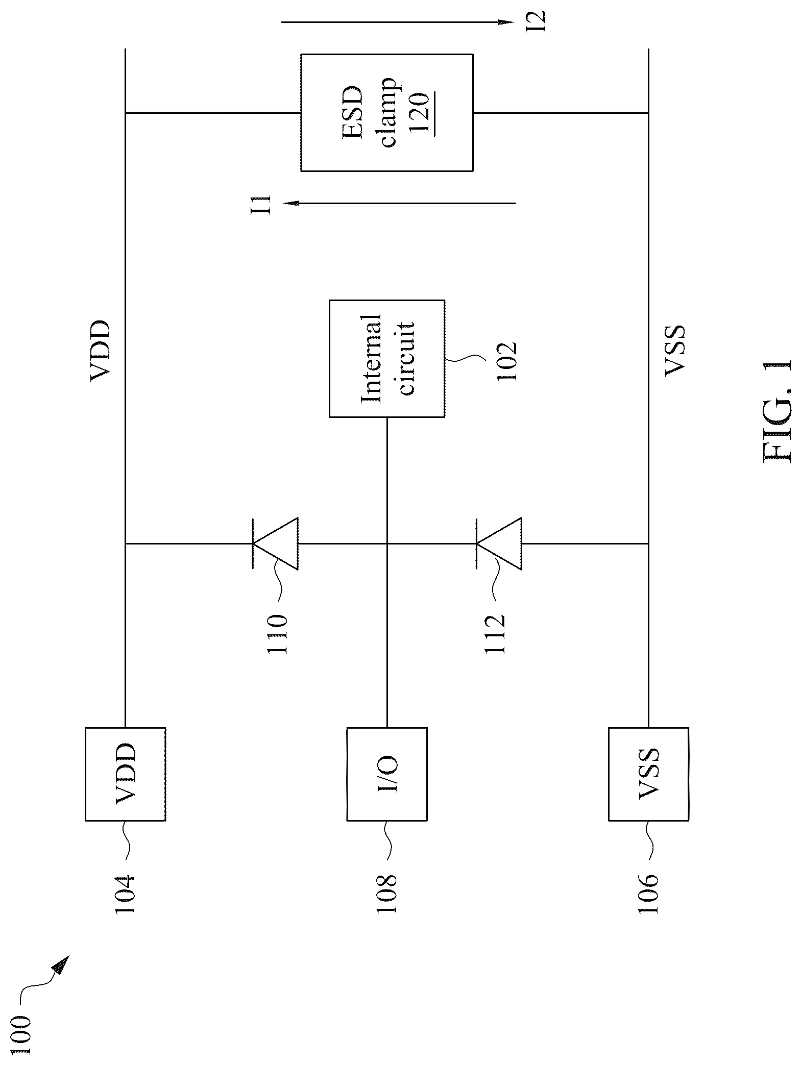
is a schematic block diagram of an integrated circuit 100 , in accordance with some embodiments.
Integrated circuit 100 comprises an internal circuit 102 , a voltage supply node 104 , a reference voltage supply node 106 , an input/output (IO) pad 108 , a diode 110 , a diode 112 and an ESD clamp 120 . In some embodiments, at least integrated circuit 100 , 200 A- 200 E ( A- 2 E ), 300 A- 300 E ( A- 3 E ), 400 A- 400 E ( A- 4 E ), 500 A- 500 E ( A- 5 E ), 600 A- 600 B ( A- 6 B ), 700 A- 700 B ( A- 7 B ) or 800 A- 800 B ( A- 8 B ) is incorporated on a single integrated circuit (IC), or on a single semiconductor substrate. In some embodiments, at least integrated circuit 100 , 200 A- 200 E ( A- 2 E ), 300 A- 300 E ( A- 3 E ), 400 A- 400 E ( A- 4 E ), 500 A- 500 E ( A- 5 E ), 600 A- 600 B ( A- 6 B ), 700 A- 700 B ( A- 7 B ) or 800 A- 800 B ( A- 8 B ) includes one or more ICs incorporated on one or more single semiconductor substrate.
Internal circuit 102 is coupled to the IO pad 108 , diode 110 and diode 112 . Internal circuit 102 is configured to receive an IO signal from IO pad 108 . In some embodiments, internal circuit 102 is coupled to voltage supply node 104 (e.g., VDD) and reference voltage supply node 106 (e.g., VSS). In some embodiments, internal circuit 102 is configured to receive a supply voltage VDD from voltage supply node 104 (e.g., VDD), and a reference voltage VSS from reference voltage supply node 106 (e.g., VSS).
Internal circuit 102 includes circuitry configured to generate or process the IO signal received by or output to IO pad 108 . In some embodiments, internal circuit 102 comprises core circuitry configured to operate at a voltage lower than supply voltage VDD of voltage supply node 104 . In some embodiments, internal circuit 102 includes at least one n-type or p-type transistor device. In some embodiments, internal circuit 102 includes at least a logic gate cell. In some embodiments, a logic gate cell includes an AND, OR, NAND, NOR, XOR, INV, AND-OR-Invert (AOI), OR-AND-Invert (OAI), MUX, Flip-flop, BUFF, Latch, delay, or clock cells. In some embodiments, internal circuit 102 includes at least a memory cell. In some embodiments, the memory cell includes a static random access memory (SRAM), a dynamic RAM (DRAM), a resistive RAM (RRAM), a magnetoresistive RAM (MRAM) or read only memory (ROM). In some embodiments, internal circuit 102 includes one or more active or passive elements. Examples of active elements include, but are not limited to, transistors and diodes. Examples of transistors include, but are not limited to, metal oxide semiconductor field effect transistors (MOSFET), complementary metal oxide semiconductor (CMOS) transistors, bipolar junction transistors (BJT), high voltage transistors, high frequency transistors, p-channel and/or n-channel field effect transistors (PFETs/NFETs), or the like), FinFETs, and planar MOS transistors with raised source/drain. Examples of passive elements include, but are not limited to, capacitors, inductors, fuses, and resistors.
Voltage supply node 104 is coupled to diode 110 and ESD clamp 120 . Reference voltage supply node 106 is coupled to diode 112 and ESD clamp 120 . Voltage supply node 104 is configured to receive supply voltage VDD for normal operation of internal circuit 102 . Similarly, reference voltage supply node 106 is configured to receive reference supply voltage VSS for normal operation of internal circuit 102 . In some embodiments, at least voltage supply node 104 is a voltage supply pad. In some embodiments, at least reference voltage supply node 106 is a reference voltage supply pad. In some embodiments, a pad is at least a conductive surface, a pin, a node or a bus. Voltage supply node 104 or reference voltage supply node 106 is also referred to as a power supply voltage bus or rail. In the example configuration in , 2 A- 2 E, 3 A- 3 E, 4 A- 4 E, 5 A- 5 E, 6 A- 6 B, 7 A- 7 B or 8 A- 8 B supply voltage VDD is a positive supply voltage, voltage supply node 104 is a positive power supply voltage, reference supply voltage VSS is a ground supply voltage, and reference voltage supply node 106 is a ground voltage terminal. Other power supply arrangements are within the scope of the present disclosure.
IO pad 108 is coupled to internal circuit 102 . IO pad 108 is configured to receive IO signal from internal circuit 102 or configured to output IO signal to internal circuit 102 . IO pad 108 is at least a pin that is coupled to internal circuit 102 . In some embodiments, IO pad 108 is a node, a bus or a conductive surface that is coupled to internal circuit 102 .
Diode 110 is coupled between voltage supply node 104 and IO pad 108 . An anode of diode 110 is coupled to internal circuit 102 , IO pad 108 and a cathode of diode 112 . A cathode of diode 110 is coupled to voltage supply node 104 and ESD clamp 120 . In some embodiments, diode 110 is a pull-up diode or referred to as a p+ diode. For example, in these embodiments, the p+-diode is formed between a p-well region (not shown) and an n-well region (not shown), and the n-well region is connected to VDD.
Diode 112 is coupled between reference voltage supply node 106 and IO pad 108 . An anode of diode 112 is coupled to reference voltage supply node 106 and ESD clamp 120 . A cathode of diode 112 is coupled to internal circuit 102 , IO pad 108 and the anode of diode 110 . In some embodiments, diode 112 is a pull-down diode or referred to as an n+ diode. For example, in these embodiments, the n+-diode is formed between an n+ junction (not shown) and a p-substrate (not shown), and the P-substrate is connected to ground or VSS.
Diodes 110 and 112 are configured to have a minimal impact on the normal behavior (e.g., no ESD conditions or events) of internal circuit 102 or integrated circuit 100 . In some embodiments, an ESD event occurs when an ESD voltage or current higher than a level of voltage or current expected during the normal operation of internal circuit 102 is applied to at least voltage supply node 104 , reference voltage supply node 106 or IO pad 108 .
When no ESD events occur, diodes 110 and 112 do not affect the operation of integrated circuit 100 . During an ESD event, diode 110 is configured to transfer voltage or current between voltage supply node 104 and IO pad 108 dependent upon whether diode 110 is forward biased or reverse biased, and the voltage levels of the voltage supply node 104 and IO pad 108 .
For example, during a Positive-to-VDD (PD) mode of ESD stress or event, diode 110 is forward biased and is configured to transfer voltage or current from IO pad 108 to voltage supply node 104 . In PD-mode, a positive ESD stress or ESD voltage (at least greater than supply voltage VDD) is applied to IO pad 108 , while voltage supply node 104 (e.g., VDD) is ground and reference voltage supply node 106 (e.g., VSS) is floating.
For example, during a Negative-to-VDD (ND) mode of ESD stress or event, diode 110 is reverse biased and is configured to transfer voltage or current from voltage supply node 104 to IO pad 108 . In ND-mode, a negative ESD stress is received by IO pad 108 , while the voltage supply node 104 (e.g., VDD) is ground and reference voltage supply node 106 (e.g., VSS) is floating.
During an ESD event, diode 112 is configured to transfer voltage or current between reference voltage supply node 106 and IO pad 108 dependent upon whether diode 112 is forward biased or reverse biased, and the voltage levels of the reference voltage supply node 106 and IO pad 108 .
For example, during a Positive-to-VSS (PS) mode of ESD stress or event, diode 112 is reverse biased and is configured to transfer voltage or current from IO pad 108 to reference voltage supply node 106 . In PS-mode, a positive ESD stress or ESD voltage (at least greater than reference supply voltage VSS) is applied to IO pad 108 , while voltage supply node 104 (e.g., VDD) is floating and reference voltage supply node 106 (e.g., VSS) is ground.
For example, during a Negative-to-VSS (NS) mode of ESD stress or event, diode 112 is forward biased and is configured to transfer voltage or current from reference voltage supply node 106 to IO pad 108 . In NS-mode, a negative ESD stress is received by IO pad 108 , while the voltage supply node 104 (e.g., VDD) is floating and reference voltage supply node 106 (e.g., VSS) is ground.
Other types of diodes, configurations and arrangements of at least diode 110 or 112 are within the scope of the present disclosure.
ESD clamp 120 is coupled between voltage supply node 104 (e.g., supply voltage VDD) and reference voltage supply node 106 (e.g., VSS). When no ESD event occurs, ESD clamp 120 is turned off. For example, when no ESD event occurs, ESD clamp 120 is turned off, and is therefore a nonconductive device or circuit during the normal operation of internal circuit 102 . In other words, ESD clamp 120 is turned off or is non-conductive in the absence of an ESD event.
If an ESD event occurs, ESD clamp 120 is configured to sense the ESD event, and is configured to turn on and provide a current shunt path between voltage supply node 104 (e.g., supply voltage VDD) and reference voltage supply node 106 (e.g., VSS) to thereby discharge the ESD current. For example, when an ESD event occurs, the voltage difference across the ESD clamp 120 is equal to or greater than a threshold voltage of ESD clamp 120 , and ESD clamp 120 is turned ON thereby conducting current between voltage supply node 104 (e.g., VDD) and reference voltage supply node 106 (e.g., VSS).
During an ESD event, ESD clamp 120 is configured to turn on and discharge an ESD current (I 1 or I 2 ) in a forward ESD direction (e.g., current I 1 ) or a reverse ESD direction (e.g., current I 2 ). The forward ESD direction (e.g., current I 1 ) is from the reference voltage supply node 106 (e.g., VSS) to the voltage supply node 104 (e.g., VDD). The reverse ESD direction (e.g., current I 2 ) is from voltage supply node 104 (e.g., VDD) to reference voltage supply node 106 (e.g., VSS).
During a positive ESD surge on reference voltage supply node 106 , ESD clamp 120 is configured to turn on and discharge the ESD current I 1 in a forward ESD direction from the reference voltage supply node 106 (e.g., VSS) to the voltage supply node 104 (e.g., VDD). In some embodiments, ESD clamp 120 is configured to turn on, after a PS mode (described above) of ESD, and discharge the ESD current I 1 in the forward ESD direction from the reference voltage supply node 106 (e.g., VSS) to the voltage supply node 104 (e.g., VDD).
During a positive ESD surge on voltage supply node 104 , ESD clamp 120 is configured to turn on and discharge the ESD current I 2 in a reverse ESD direction from voltage supply node 104 (e.g., VDD) to reference voltage supply node 106 (e.g., VSS). In some embodiments, ESD clamp 120 is configured to turn on, after a PD mode (described above) of ESD, and discharge the ESD current I 2 in the reverse ESD direction from voltage supply node 104 (e.g., VDD) to reference voltage supply node 106 (e.g., VSS).
In some embodiments, ESD clamp 120 is a transient clamp. For example, in some embodiments, ESD clamp 120 is configured to handle transient or rapid ESD events, e.g., rapid changes in voltage and/or current from the ESD event. During the transient or rapid ESD, the ESD clamp 120 is configured to turn on very quickly to provide a shunt path between voltage supply node 104 (e.g., supply voltage VDD) and reference voltage supply node 106 (e.g., VSS) before the ESD event can cause damage to one or more elements within integrated circuit 100 . In some embodiments, ESD clamp 120 is configured to turn off slower than it turns on.
In some embodiments, ESD clamp 120 is a static clamp. In some embodiments, static clamps are configured to provide a static or steady-state voltage and current response. For example, static clamps are turned-on by a fixed voltage level.
In some embodiments, ESD clamp 120 includes a large NMOS transistor or PMOS transistor configured to carry the ESD current without entering the avalanche breakdown region of the ESD clamp 120 . In some embodiments, ESD clamp 120 is implemented without having avalanching junctions inside ESD clamp 120 , and is also known as a “non-snapback protection scheme.”
Other types of clamp circuits, configurations and arrangements of ESD clamp 120 are within the scope of the present disclosure.
Other configurations or quantities of circuits in integrated circuit 100 are within the scope of the present disclosure.
In some embodiments, during an ESD event at the first node or the second node, the ESD clamp 120 is configured to discharge an ESD current of the ESD event in the forward ESD direction from the second node to the first node, in accordance with some embodiments. In comparison with other approaches in the forward ESD direction, integrated circuit 100 has better ESD discharging capability and performance while occupying less area.
A is a circuit diagram of an integrated circuit 200 A, in accordance with some embodiments.
Integrated circuit 200 A is an embodiment of ESD clamp 120 , and similar detailed description is therefore omitted.
Components that are the same or similar to those in one or more of , 2 A- 2 E, 3 A- 3 E, 4 A- 4 E, 5 A- 5 E, 6 A- 6 B, 7 A- 7 B and 8 A- 8 B (shown below) are given the same reference numbers, and detailed description thereof is thus omitted.
Node Nd 1 in A- 2 E, 3 A- 3 E, 4 A- 4 E, 5 A- 5 E, 6 A- 6 B, 7 A- 7 B and 8 A- 8 B corresponds to voltage supply node 104 of . Node Nd 2 of A- 2 E, 3 A- 3 E, 4 A- 4 E, 5 A- 5 E, 6 A- 6 B, 7 A- 7 B and 8 A- 8 B corresponds to reference voltage supply node 106 of .
Integrated circuit 200 A includes a control circuit 201 , an ESD detection circuit 202 , an ESD assist circuit 204 a and a discharging circuit 210 .
Control circuit 201 is coupled to ESD detection circuit 202 , ESD assist circuit 204 a , and discharging circuit 210 by nodes Nd 1 and Nd 2 . Control circuit 201 is further coupled between node Nd 1 and node Nd 2 . Control circuit 201 is configured to control at least ESD detection circuit 202 .
ESD detection circuit 202 is coupled to control circuit 201 , ESD assist circuit 204 a , discharging circuit 210 and a node Nd 3 . ESD detection circuit 202 is further coupled between node Nd 1 and node Nd 2 . ESD detection circuit 202 is configured to detect an ESD event at node Nd 2 (e.g., ESD current I 1 in the forward ESD direction), and to charge node Nd 3 in response to the ESD event, thereby turning on discharging circuit 210 . In some embodiments, in response to being turned on, discharging circuit 210 couples node Nd 1 and Nd 2 thereby providing an ESD discharge path between node Nd 1 and Nd 2 . In some embodiments, ESD detection circuit 202 is configured to detect an ESD event at node Nd 1 (e.g., ESD current I 2 in the reverse ESD direction).
ESD assist circuit 204 a is coupled to node Nd 1 , node Nd 3 , ESD detection circuit 202 and discharging circuit 210 . In response to an ESD event at node Nd 2 (e.g., an ESD current I 1 in the forward ESD direction), ESD assist circuit 204 a is configured to turn-on and clamp a voltage at node Nd 3 to be equal to a voltage of node Nd 1 (e.g., VDD) thereby assisting the detection circuit 204 in causing the discharging circuit 210 to turn-on. In some embodiments, in response to being turned on, discharging circuit 210 couples node Nd 2 and Nd 1 thereby providing a forward ESD discharge path between node Nd 2 and Nd 1 .
Discharging circuit 210 is coupled between node Nd 1 and node Nd 2 . Discharging circuit 210 is further coupled to node Nd 3 , ESD detection circuit 202 and ESD assist circuit 204 a . Discharging circuit 210 is configured to couple node Nd 1 and Nd 2 during an ESD event at node Nd 1 or node Nd 2 , thereby providing an ESD discharge path between node Nd 1 and Nd 2 .
ESD detection circuit 202 includes a resistor R 1 , a capacitor C 1 , an N-type Metal Oxide Semiconductor (NMOS) transistor N 1 and a P-type Metal Oxide Semiconductor (PMOS) transistor P 1 .
Discharging circuit 210 includes a PMOS transistor P 2 . PMOS transistor P 2 includes a gate, a drain and a source (not labelled).
ESD assist circuit 204 a includes a PMOS transistor P 3 . In some embodiments, PMOS transistor P 3 is a grounded gate PMOS (ggPMOS) transistor. PMOS transistor P 3 includes a gate, a drain and a source (not labelled).
Each of a first end of resistor R 1 , node Nd 2 , a source of NMOS transistor N 1 , a body of NMOS transistor N 1 and a drain of PMOS transistor P 2 are coupled together.
Each of a second end of resistor R 1 , node Nd 4 , a first end of capacitor C 1 , a gate of PMOS transistor P 1 , and a gate of NMOS transistor N 2 are coupled together.
Each of a second end of capacitor C 1 , node Nd 1 , a source of PMOS transistor P 1 , a body of PMOS transistor P 1 , a source of PMOS transistor P 2 , a body of PMOS transistor P 2 , a source of PMOS transistor P 3 , a gate of PMOS transistor P 3 , and a body of PMOS transistor P 3 are coupled together.
Each of a node Nd 3 , a drain of NMOS transistor N 1 , a drain of PMOS transistor P 1 , a source of PMOS transistor P 3 and a gate of PMOS transistor P 2 are coupled together.
In some embodiments, capacitor C 1 is a transistor-coupled capacitor. For example in some embodiments, capacitor C 1 is a transistor having a drain and source coupled together thereby forming a transistor-coupled capacitor.
Resistor R 1 and capacitor C 1 are configured as an RC network. Depending upon a location of an output of the RC network, the RC network is configured as either a low pass filter or a high pass filter.
NMOS transistor N 1 and PMOS transistor P 1 are configured as an inverter (not labelled). Thus, a slowly rising voltage at node Nd 4 will be inverted by NMOS transistor N 1 and PMOS transistor P 1 (e.g., an inverter) thereby causing node Nd 3 to rapidly rise. Furthermore, a rapidly rising voltage at node Nd 4 will be inverted by NMOS transistor N 1 and PMOS transistor P 1 (e.g., an inverter) thereby causing node Nd 3 to rise slowly. In some embodiments, NMOS transistor N 1 and PMOS transistor P 1 are configured to generate an inverted input signal (not shown) in response to an input signal (not shown).
When an ESD event at node Nd 2 occurs (e.g., ESD current I 1 in the forward ESD direction), the ESD current or voltage at node Nd 2 rises rapidly causing the voltage of node Nd 4 (e.g., across resistor R 1 ) to rise rapidly since the voltage at node Nd 4 corresponds to an output voltage of a high pass filter (e.g., a voltage across resistor R 1 with respect to node Nd 2 ). In other words, resistor R 1 is configured as a high pass filter, and the rapidly changing voltage or current from the ESD event is not filtered or is passed by resistor R 1 . In response to the rapidly rising voltage at node Nd 4 , PMOS transistor P 1 and NMOS transistor N 1 are configured as an inverter thereby inverting the voltage of node Nd 4 to the voltage of node Nd 3 , and the voltage of Nd 3 is rapidly falling. Stated differently, the voltage of node Nd 3 is inverted from the voltage of node Nd 4 . In some embodiments, in response to the voltage at node Nd 4 , PMOS transistor P 3 turns on, and is configured to clamp a voltage at node Nd 3 to be equal to a voltage of node Nd 1 (e.g., VDD) thereby assisting the ESD detection circuit 202 in causing the PMOS transistor P 2 to turn-on. In response to being turned on, PMOS transistor P 2 couples node Nd 2 to node Nd 1 and NMOS transistor N 2 discharges the ESD current I 1 in the forward ESD direction from node Nd 2 to Nd 1 .
In some embodiments, by including ESD assist circuit 204 a in integrated circuit 200 A, the PMOS transistor P 3 of ESD assist circuit 204 a is configured to control the gate potential of PMOS transistor P 2 by clamping the voltage of node Nd 3 to be equal to the voltage of node Nd 1 (e.g., VDD) during an ESD event at node Nd 2 thereby reducing capacitive coupling effects between node Nd 2 and Nd 3 and effectively lowering the turn-on resistance of PMOS transistor P 2 , and thus causing the PMOS transistor P 2 to turn-on faster and stronger than other approaches resulting in improved ESD performance and improved ESD robustness compared to other approaches.
In some embodiments, in response to an ESD event at node Nd 2 (e.g., an ESD current I 1 in the forward ESD direction), a body diode of the PMOS transistor P 3 is configured to provide ESD protection of integrated circuit 200 A by clamping the voltage of node Nd 3 . In some embodiments, a body diode of the PMOS transistor P 2 is configured to provide ESD protection of integrated circuit 200 A by passing the ESD current I 1 in the forward ESD direction from node Nd 2 to node Nd 1 .
In some embodiments, ESD assist circuit 204 a has a minimal effect on an ESD event at node Nd 1 . For example, in some embodiments, when an ESD event at node Nd 1 occurs, PMOS transistor P 3 is turned off.
Other types of circuits, configurations and arrangements of at least ESD detection circuit 202 , ESD assist circuit 204 a or discharging circuit 210 are within the scope of the present disclosure.
Other configurations or quantities of circuits in integrated circuit 200 A are within the scope of the present disclosure.
B is a circuit diagram of an integrated circuit 200 B, in accordance with some embodiments.
Integrated circuit 200 B is an embodiment of at least ESD clamp 120 , and similar detailed description is therefore omitted.
Integrated circuit 200 B is a variation of integrated circuit 200 A of A , and similar detailed description is therefore omitted. In comparison with integrated circuit 200 A, ESD assist circuit 204 b of integrated circuit 200 B replaces ESD assist circuit 204 a of integrated circuit 200 A, and similar detailed description is therefore omitted.
Integrated circuit 200 B includes control circuit 201 , ESD detection circuit 202 , ESD assist circuit 204 b and discharging circuit 210 .
ESD assist circuit 204 b is a variation of ESD assist circuit 204 a of A , and similar detailed description is therefore omitted. In comparison with ESD assist circuit 204 a , a diode D 1 of ESD assist circuit 204 b replaces PMOS transistor P 3 of ESD assist circuit 204 a , and similar detailed description is therefore omitted.
ESD assist circuit 204 b includes diode D 1 . Diode D 1 includes an anode and a cathode (not labelled).
In comparison with ESD assist circuit 204 a of A , each of the anode of diode D 1 , node Nd 3 , a drain of NMOS transistor N 1 , a drain of PMOS transistor P 1 and a gate of PMOS transistor P 2 are coupled together.
In comparison with ESD assist circuit 204 a of A , each of the cathode of diode D 1 , the second end of capacitor C 1 , node Nd 1 , the source of PMOS transistor P 1 , the body of PMOS transistor P 1 , the source of PMOS transistor P 2 and the body of PMOS transistor P 2 are coupled together.
The description for when an ESD event occurs at node Nd 2 (e.g., ESD current I 1 in the forward ESD direction) with ESD assist circuit 204 b for B is similar to the description of when an ESD event occurs at node Nd 2 for ESD assist circuit 204 a of A , and similar detailed description is therefore omitted for brevity. In some embodiments, in response to an ESD event at node Nd 2 (e.g., an ESD current I 1 in the forward ESD direction), diode D 1 is configured to be forward-biased and thereby clamps the voltage at node Nd 3 to be equal to a voltage of node Nd 1 (e.g., VDD) thereby assisting the ESD detection circuit 202 in causing the PMOS transistor P 2 to turn-on. In response to being turned on, PMOS transistor P 2 couples node Nd 2 to node Nd 1 and PMOS transistor P 2 discharges the ESD current I 1 in the forward ESD direction from node Nd 2 to Nd 1 .
In some embodiments, by including ESD assist circuit 204 b in integrated circuit 200 B, integrated circuit 200 B achieves one or more of the benefits discussed above in at least or A .
Other types of circuits, configurations and arrangements of at least ESD detection circuit 202 , ESD assist circuit 204 b or discharging circuit 210 are within the scope of the present disclosure.
Other configurations or quantities of circuits in integrated circuit 200 B are within the scope of the present disclosure.
C is a circuit diagram of an integrated circuit 200 C, in accordance with some embodiments.
Integrated circuit 200 C is an embodiment of at least ESD clamp 120 , and similar detailed description is therefore omitted.
Integrated circuit 200 C is a variation of integrated circuit 200 A of A , and similar detailed description is therefore omitted. In comparison with integrated circuit 200 A, ESD assist circuit 204 c of integrated circuit 200 C replaces ESD assist circuit 204 a of integrated circuit 200 A, and similar detailed description is therefore omitted.
Integrated circuit 200 C includes control circuit 201 , ESD detection circuit 202 , ESD assist circuit 204 c and discharging circuit 210 .
ESD assist circuit 204 c is a variation of ESD assist circuit 204 a of A , and similar detailed description is therefore omitted. In comparison with ESD assist circuit 204 a , a transistor B 1 of ESD assist circuit 204 c replaces PMOS transistor P 3 of ESD assist circuit 204 a , and similar detailed description is therefore omitted. Transistor B 1 is a PNP bipolar junction transistor (BJT).
ESD assist circuit 204 c includes transistor B 1 . Transistor B 1 includes a base, a collector and an emitter (not labelled).
In comparison with ESD assist circuit 204 a of A , each of the collector of transistor B 1 , node Nd 3 , a drain of NMOS transistor N 1 , a drain of PMOS transistor P 1 and a gate of PMOS transistor P 2 are coupled together.
In comparison with ESD assist circuit 204 a of A , each of the emitter of transistor B 1 , the base of transistor B 1 , the second end of capacitor C 1 , node Nd 1 , the source of PMOS transistor P 1 , the body of PMOS transistor P 1 , the source of PMOS transistor P 2 and the body of PMOS transistor P 2 are coupled together.
The description for when an ESD event occurs at node Nd 2 (e.g., ESD current I 1 in the forward ESD direction) with ESD assist circuit 204 c for C is similar to the description of when an ESD event occurs at node Nd 2 for ESD assist circuit 204 a of A , and similar detailed description is therefore omitted for brevity. In some embodiments, in response to an ESD event at node Nd 2 (e.g., an ESD current I 1 in the forward ESD direction), transistor B 1 turns on, and is configured to clamp a voltage at node Nd 3 to be equal to a voltage of node Nd 1 (e.g., VDD) thereby assisting the ESD detection circuit 202 in causing the PMOS transistor P 2 to turn-on. In response to being turned on, PMOS transistor P 2 couples node Nd 2 to node Nd 1 , and PMOS transistor P 2 discharges the ESD current I 1 in the forward ESD direction from node Nd 2 to Nd 1 .
In some embodiments, in response to an ESD event at node Nd 2 (e.g., an ESD current I 1 in the forward ESD direction), a body diode of transistor B 1 is configured to provide ESD protection of integrated circuit 200 C by clamping the voltage of node Nd 3 . In some embodiments, a body diode of PMOS transistor P 2 is configured to provide ESD protection of integrated circuit 200 C by passing the ESD current I 1 in the forward ESD direction from node Nd 2 to node Nd 1 .
In some embodiments, by including ESD assist circuit 204 c in integrated circuit 200 C, integrated circuit 200 C achieves one or more of the benefits discussed above in at least or A .
Other types of circuits, configurations and arrangements of at least ESD detection circuit 202 , ESD assist circuit 204 c or discharging circuit 210 are within the scope of the present disclosure.
Other configurations or quantities of circuits in integrated circuit 200 C are within the scope of the present disclosure.
D is a circuit diagram of an integrated circuit 200 D, in accordance with some embodiments.
Integrated circuit 200 D is an embodiment of at least ESD clamp 120 , and similar detailed description is therefore omitted.
Integrated circuit 200 D is a variation of integrated circuit 200 A of A , and similar detailed description is therefore omitted. In comparison with integrated circuit 200 A, ESD assist circuit 204 d of integrated circuit 200 D replaces ESD assist circuit 204 a of integrated circuit 200 A, and similar detailed description is therefore omitted.
Integrated circuit 200 D includes control circuit 201 , ESD detection circuit 202 , ESD assist circuit 204 d and discharging circuit 210 .
ESD assist circuit 204 d is a variation of ESD assist circuit 204 a of A , and similar detailed description is therefore omitted. In comparison with ESD assist circuit 204 a , an NMOS transistor N 2 of ESD assist circuit 204 d replaces PMOS transistor P 3 of ESD assist circuit 204 a , and similar detailed description is therefore omitted.
ESD assist circuit 204 d includes NMOS transistor N 2 . NMOS transistor N 2 includes a gate, a drain, a source and a body (not labelled).
In comparison with ESD assist circuit 204 a of A , each of the gate of NMOS transistor N 2 , the source of NMOS transistor N 2 , the body of NMOS transistor N 2 , node Nd 3 , a drain of NMOS transistor N 1 , a drain of PMOS transistor P 1 and a gate of PMOS transistor P 2 are coupled together.
In comparison with ESD assist circuit 204 a of A , each of the drain of NMOS transistor N 2 , the second end of capacitor C 1 , node Nd 1 , the source of PMOS transistor P 1 , the body of PMOS transistor P 1 , the source of PMOS transistor P 2 and the body of PMOS transistor P 2 are coupled together.
The description for when an ESD event occurs at node Nd 2 (e.g., ESD current I 1 in the forward ESD direction) with ESD assist circuit 204 d for D is similar to the description of when an ESD event occurs at node Nd 2 for ESD assist circuit 204 a of A , and similar detailed description is therefore omitted for brevity. In some embodiments, in response to an ESD event at node Nd 2 (e.g., an ESD current I 1 in the forward ESD direction), NMOS transistor N 2 turns on, and is configured to clamp a voltage at node Nd 3 to be equal to a voltage of node Nd 1 (e.g., VDD) thereby assisting the ESD detection circuit 202 in causing the PMOS transistor P 2 to turn-on. In response to being turned on, PMOS transistor P 2 couples node Nd 2 to node Nd 1 , and PMOS transistor P 2 discharges the ESD current I 1 in the forward ESD direction from node Nd 2 to Nd 1 .
In some embodiments, in response to an ESD event at node Nd 2 (e.g., an ESD current I 1 in the forward ESD direction), a body diode of NMOS transistor N 2 is configured to provide ESD protection of integrated circuit 200 D by clamping the voltage of node Nd 3 . In some embodiments, a body diode of PMOS transistor P 2 is configured to provide ESD protection of integrated circuit 200 D by passing the ESD current I 1 in the forward ESD direction from node Nd 2 to node Nd 1 .
In some embodiments, by including ESD assist circuit 204 d in integrated circuit 200 D, integrated circuit 200 D achieves one or more of the benefits discussed above in at least or A .
Other types of circuits, configurations and arrangements of at least ESD detection circuit 202 , ESD assist circuit 204 d or discharging circuit 210 are within the scope of the present disclosure.
Other configurations or quantities of circuits in integrated circuit 200 D are within the scope of the present disclosure.
E is a circuit diagram of an integrated circuit 200 E, in accordance with some embodiments.
Integrated circuit 200 E is an embodiment of at least ESD clamp 120 , and similar detailed description is therefore omitted.
Integrated circuit 200 E is a variation of integrated circuit 200 A of A , and similar detailed description is therefore omitted. In comparison with integrated circuit 200 A, ESD assist circuit 204 e of integrated circuit 200 E replaces ESD assist circuit 204 a of integrated circuit 200 A, and similar detailed description is therefore omitted.
Integrated circuit 200 E includes control circuit 201 , ESD detection circuit 202 , ESD assist circuit 204 e and discharging circuit 210 .
ESD assist circuit 204 e is a variation of ESD assist circuit 204 a of A , and similar detailed description is therefore omitted. In comparison with ESD assist circuit 204 a , a transistor B 2 of ESD assist circuit 204 e replaces PMOS transistor P 3 of ESD assist circuit 204 a , and similar detailed description is therefore omitted. Transistor B 2 is a NPN BJT.
ESD assist circuit 204 e includes transistor B 2 . Transistor B 2 includes a base, a collector and an emitter (not labelled).
In comparison with ESD assist circuit 204 a of A , each of the emitter of transistor B 2 , the base of transistor B 2 , node Nd 3 , a drain of NMOS transistor N 1 , a drain of PMOS transistor P 1 and a gate of PMOS transistor P 2 are coupled together.
In comparison with ESD assist circuit 204 a of A , each of the collector of transistor B 2 , the second end of capacitor C 1 , node Nd 1 , the source of PMOS transistor P 1 , the body of PMOS transistor P 1 , the source of PMOS transistor P 2 and the body of PMOS transistor P 2 are coupled together.
The description for when an ESD event occurs at node Nd 2 (e.g., ESD current I 1 in the forward ESD direction) with ESD assist circuit 204 e for E is similar to the description of when an ESD event occurs at node Nd 2 for ESD assist circuits 204 a and 204 c of corresponding A and 2 C , and similar detailed description is therefore omitted for brevity. In some embodiments, in response to an ESD event at node Nd 2 (e.g., an ESD current I 1 in the forward ESD direction), transistor B 2 turns on, and is configured to clamp a voltage at node Nd 3 to be equal to a voltage of node Nd 1 (e.g., VDD) thereby assisting the ESD detection circuit 202 in causing the PMOS transistor P 2 to turn-on. In response to being turned on, PMOS transistor P 2 couples node Nd 2 to node Nd 1 , and PMOS transistor P 2 discharges the ESD current I 1 in the forward ESD direction from node Nd 2 to Nd 1 .
In some embodiments, in response to an ESD event at node Nd 2 (e.g., an ESD current I 1 in the forward ESD direction), a body diode of transistor B 2 is configured to provide ESD protection of integrated circuit 200 E by clamping the voltage of node Nd 3 . In some embodiments, a body diode of PMOS transistor P 2 is configured to provide ESD protection of integrated circuit 200 E by passing the ESD current I 1 in the forward ESD direction from node Nd 2 to node Nd 1 .
In some embodiments, by including ESD assist circuit 204 e in integrated circuit 200 E, integrated circuit 200 E achieves one or more of the benefits discussed above in at least or A .
Other types of circuits, configurations and arrangements of at least ESD detection circuit 202 , ESD assist circuit 204 e or discharging circuit 210 are within the scope of the present disclosure.
Other configurations or quantities of circuits in integrated circuit 200 E are within the scope of the present disclosure.
A is a cross-sectional view of an integrated circuit 300 A, in accordance with some embodiments.
Integrated circuit 300 A is an embodiment of PMOS transistor P 3 of ESD assist circuit 204 a of A , and similar detailed description is therefore omitted.
Integrated circuit 300 A includes a substrate 302 b.
Substrate 302 b is an n-type substrate. In some embodiments, substrate 302 b is a p-type substrate. In some embodiments, substrate 302 b includes an elemental semiconductor including silicon or germanium in crystal, polycrystalline, or an amorphous structure; a compound semiconductor including silicon carbide, gallium arsenic, gallium phosphide, indium phosphide, indium arsenide, and indium antimonide; an alloy semiconductor including SiGe, GaAsP, AlInAs, AlGaAs, GaInAs, GaInP, and GaInAsP; any other suitable material; or combinations thereof. In some embodiments, the alloy semiconductor substrate has a gradient SiGe feature in which the Si and Ge composition change from one ratio at one location to another ratio at another location of the gradient SiGe feature. In some embodiments, the alloy SiGe is formed over a silicon substrate. In some embodiments, substrate 302 b is a strained SiGe substrate. In some embodiments, the semiconductor substrate has a semiconductor on insulator structure, such as a silicon on insulator (SOI) structure. In some embodiments, the semiconductor substrate includes a doped epi layer or a buried layer. In some embodiments, the compound semiconductor substrate has a multilayer structure, or the substrate includes a multilayer compound semiconductor structure.
In some embodiments, substrate 302 b is replaced with an N-well that is formed inside a p-type substrate. In some embodiments, the N-well has N-type dopants, and the p-type substrate has p-type dopants.
Integrated circuit 300 A further includes a gate structure 330 that is over substrate 302 b . The gate structure 330 includes a gate dielectric 322 and a gate electrode 330 a . Integrated circuit 300 A further includes sidewalls 320 a and 320 b on opposite sides of gate structure 330 .
Integrated circuit 300 A further includes a drain region 312 a and a source region 314 a . The source region 314 a is a P+ active region having P-type dopants implanted in the well (not shown) or substrate 302 b . The drain region 312 a is a P+ active region having P-type dopants implanted in well (not shown) or substrate 302 b . In some embodiments, at least source region 314 a or drain region 312 a extends above substrate 302 b.
In some embodiments, the drain region 312 a and source region 314 a of transistor 360 a of A or active regions of other devices of B- 2 E and 4 A- 4 E are referred to as an oxide definition (OD) region which defines active regions of integrated circuits 300 A- 300 E and 400 A- 400 E (described below).
In some embodiments, integrated circuit 300 A further includes lightly doped drain (LDD) regions 318 adjacent to source region 314 a and drain region 312 a , and below sidewalls 320 . In some embodiments, a first element and a second element are adjacent to each other includes scenarios where the first element and the second element are directly next to each other. In some embodiments, a first element and a second element are adjacent to each other includes scenarios where intermediary elements are positioned between the first element and the second element. In some embodiments, LDD region 360 helps transistor 360 a maintain a low leakage current.
In some embodiments, drain region 312 a , source region 314 a , LDD regions 318 , sidewalls 320 and gate structure 330 together form a transistor 360 a . Transistor 360 a is a PMOS transistor.
Drain region 312 a corresponds to the drain of PMOS transistor P 3 of A , source region 314 a corresponds to the source of PMOS transistor P 3 of A , gate structure 330 corresponds to the gate of PMOS transistor P 3 of A , and tap regions 316 a and 317 a correspond to the body of PMOS transistor P 3 of A , and similar detailed description is therefore omitted.
The drain region 312 a is coupled to node Nd 3 (shown in A ). The gate structure 330 , the source region 314 a and the tap regions 316 a and 316 b are coupled to the supply voltage (e.g., voltage VDD) by node Nd 1 . In some embodiments, each of the gate structure 330 , source region 314 a and tap regions 316 a and 316 b are coupled together at node Nd 1 , and are further coupled to the supply voltage (e.g., voltage VDD).
In some embodiments, drain region 312 a and source region 314 a comprise fins in accordance with fin field-effect transistor (FinFET) complementary metal-oxide-semiconductor (CMOS) technologies. In some embodiments, drain region 312 a and source region 314 a comprise nanosheets of nanosheet transistors. In some embodiments, drain region 312 a and source region 314 a comprise nanowire of nanowire transistors. In some embodiments, drain region 312 a and source region 314 a are free of fins in accordance with planar CMOS technologies. Other types of transistors are within the scope of the present disclosure.
In some embodiments, drain region 312 a is an extended drain region and has a greater size than source region 314 a . In at least one embodiment, a silicide layer (not shown) covers a portion, but not the entirety, of drain region 312 a . Such a partially silicided configuration of drain region 312 a improves self-protection of transistor 360 a from ESD events. In at least one embodiment, drain region 312 a is fully silicided.
Gate structure 330 is arranged between drain region 312 a and source region 314 a . In some embodiments, gate electrode 330 a comprises a conductive material such as metal or polysilicon (also referred to herein as “POLY”). In some embodiments, gate structure 330 is coupled to a supply voltage terminal (e.g., voltage VDD), or a reference supply voltage terminal (e.g., voltage VS S).
Integrated circuit 300 A further includes tap regions 316 a and 317 a and shallow trench isolation (STI) regions 308 , 309 , 310 and 311 .
STI region 308 is configured to isolate at least drain region 312 a and tap region 317 a from each other. In some embodiments, STI region 308 is configured to isolate drain region 312 a or tap region 317 a from other portions of integrated circuit 300 A (not shown).
STI region 309 is configured to isolate tap region 317 a from other portions of integrated circuit 300 A.
STI region 310 is configured to isolate at least source region 314 a and tap region 316 a from each other. In some embodiments, STI region 310 is configured to isolate source region 314 a or tap region 316 a from other portions of integrated circuit 300 A (not shown).
STI region 311 is configured to isolate tap region 316 a from other portions of integrated circuit 300 A.
In some embodiments, tap regions 316 a and 317 a correspond to a well tap. In some embodiments, a well tap is electrically conductive materials that couple source/drain regions of integrated circuit 300 A to a voltage supply node (e.g., supply voltage VDD).
Tap regions 316 a and 317 a are heavily doped n-regions in a well (not shown) or substrate 302 b . In some embodiments, tap regions 316 a and 317 a are heavily doped n-regions in a n-type well (not shown) on a p-type substrate. In some embodiments, the heavily doped n-region is coupled through the well tap to the voltage supply node (e.g., supply voltage VDD) thereby setting the potential of the n-type well or substrate 302 b to prevent leakage from adjacent source/drain regions into the n-well/p-substrate.
Integrated circuit 300 A further includes a body diode 340 a . Body diode 340 a is a parasitic element formed by the PN junction between the drain region 312 a and at least tap region 316 a or 317 a . In some embodiments, the body diode 340 a is formed by the PN junction between the drain region 312 a and the source region 314 a . The body diode 340 a is also referred to as a parasitic diode or an internal diode of integrated circuit 300 A. In some embodiments, in response to ESD events at node Nd 2 in the forward direction, body diode 340 a of PMOS transistor P 3 is configured to provide ESD protection of integrated circuit 300 A by clamping the voltage of node Nd 3 , and integrated circuit 300 A thereby achieves one or more of the benefits discussed above in at least or A .
B is a cross-sectional view of an integrated circuit 300 B, in accordance with some embodiments.
Integrated circuit 300 B is an embodiment of diode D 1 of ESD assist circuit 204 b of B , and similar detailed description is therefore omitted. Integrated circuit 300 B is a variation of integrated circuit 300 A of A , and similar detailed description is therefore omitted.
Integrated circuit 300 B includes a substrate 302 b , a P-type region 352 a , an N-type region 356 a , and STI regions 308 , 310 and 311 .
P-type region 352 a is similar to the drain region 312 a in A , and similar detailed description is therefore omitted.
Substrate 302 b is an n-type substrate having N-type dopants. The P-type region 352 a is a P+ active region having P-type dopants implanted in the well (not shown) or substrate 302 b . The N-type region 356 a is an N+ active region having N-type dopants implanted in the well (not shown) or substrate 302 b . STI region 310 is between P-type region 352 a and N-type region 356 a.
STI region 308 is configured to isolate at least P-type region 352 a from other portions of integrated circuit 300 B (not shown). STI region 311 is configured to isolate at least N-type region 356 a from other portions of integrated circuit 300 B (not shown).
STI region 310 is configured to isolate at least P-type region 352 a and N-type region 356 a from each other. In some embodiments, STI region 310 is configured to isolate P-type region 352 a or N-type region 356 a from other portions of integrated circuit 300 B (not shown).
P-type region 352 a corresponds to the anode of diode D 1 of B , and N-type region 356 a corresponds to the cathode of diode D 1 of B , and similar detailed description is therefore omitted.
The P-type region 352 a is coupled to node Nd 3 (shown in A ). The N-type region 356 a is coupled to the supply voltage (e.g., voltage VDD) by node Nd 1 .
Integrated circuit 300 B further includes a body diode 340 b . Body diode 340 b is a parasitic element formed by the PN junction between the P-type region 352 a and N-type region 356 a . In some embodiments, in response to ESD events at node Nd 2 in the forward direction, body diode 340 b is configured to provide ESD protection of integrated circuit 300 B by clamping the voltage of node Nd 3 , and integrated circuit 300 B thereby achieves one or more of the benefits discussed above in at least or A .
C is a cross-sectional view of an integrated circuit 300 C, in accordance with some embodiments.
Integrated circuit 300 C is an embodiment of transistor B 1 of ESD assist circuit 204 c of C , and similar detailed description is therefore omitted. Integrated circuit 300 C is a variation of integrated circuit 300 A of A , and similar detailed description is therefore omitted.
Integrated circuit 300 C includes a substrate 302 a , a P-type region 362 a , and an N-type region 366 a . Substrate 302 a is similar to substrate 302 b , P-type region 362 a is similar to P-type region 352 a in B , N-type region 366 a is similar to N-type region 356 a in B , and similar detailed description is therefore omitted.
In C , substrate 302 a is a p-type substrate having P-type dopants. The N-type region 366 a is an N+ active region having N-type dopants implanted in substrate 302 a . The P-type region 362 a is a P+ active region having P-type dopants implanted in the N-type region 366 a.
P-type region 362 a corresponds to the emitter of transistor B 1 of C , N-type region 366 a corresponds to the base of transistor B 1 of C , substrate 302 a corresponds to the collector of transistor B 1 of C , and similar detailed description is therefore omitted.
Each of the P-type region 362 a and the N-type region 366 a are coupled together, and further coupled to the supply voltage (e.g., voltage VDD) by node Nd 1 . The substrate 302 a is coupled to node Nd 3 .
Integrated circuit 300 C further includes a body diode 340 c . Body diode 340 c is a parasitic element formed by the PN junction between the substrate 302 a and the N-type region 366 a . In some embodiments, in response to ESD events at node Nd 2 in the forward direction, body diode 340 c is configured to provide ESD protection of integrated circuit 300 C by clamping the voltage of node Nd 3 , and integrated circuit 300 C thereby achieves one or more of the benefits discussed above in at least or A .
D is a cross-sectional view of an integrated circuit 300 D, in accordance with some embodiments.
Integrated circuit 300 D is an embodiment of NMOS transistor N 2 of ESD assist circuit 204 d of D , and similar detailed description is therefore omitted. Integrated circuit 300 D is a variation of integrated circuit 300 A of A , and similar detailed description is therefore omitted.
In comparison with integrated circuit 300 A of A , a drain region 312 b replaces drain region 312 a of A , a source region 314 b replaces source region 314 a of A , tap regions 316 b and 317 b replace corresponding tap regions 316 a and 317 a of A , transistor 360 b replaces transistor 360 a , and similar detailed description is therefore omitted.
Integrated circuit 300 D includes substrate 302 a , gate structure 330 , drain region 312 b , source region 314 b , LDD regions 318 , sidewalls 320 , tap regions 316 b and 317 b , and STI regions 308 , 309 , 310 and 311 , and body diode 340 d.
In D , substrate 302 a is a p-type substrate having P-type dopants.
In some embodiments, drain region 312 b , source region 314 b , LDD regions 318 , sidewalls 320 and gate structure 330 together form a transistor 360 b . Transistor 360 b is an NMOS transistor.
Drain region 312 b corresponds to the drain of NMOS transistor N 2 of D , source region 314 b corresponds to the source of NMOS transistor N 2 of D , gate structure 330 corresponds to the gate of NMOS transistor N 2 of D , and tap regions 316 b and 317 b correspond to the body of NMOS transistor N 2 of D , and similar detailed description is therefore omitted.
The drain region 312 b is coupled to the supply voltage (e.g., voltage VDD) by node Nd 1 . The gate structure 330 , the source region 314 b and the tap region 316 b are coupled to node Nd 3 .
STI region 308 is configured to isolate at least drain region 312 b and tap region 317 b from each other. In some embodiments, STI region 308 is configured to isolate drain region 312 b or tap region 317 b from other portions of integrated circuit 300 D (not shown).
STI region 309 is configured to isolate tap region 317 b from other portions of integrated circuit 300 D.
STI region 310 is configured to isolate at least source region 314 b and tap region 316 b from each other. In some embodiments, STI region 310 is configured to isolate source region 314 b or tap region 316 b from other portions of integrated circuit 300 D (not shown).
STI region 311 is configured to isolate tap region 316 b from other portions of integrated circuit 300 D.
In some embodiments, tap regions 316 b and 317 b correspond to a substrate tap. In some embodiments, a substrate tap is an electrically conductive material that couples tap regions 316 b and 317 b to a reference voltage supply node (e.g., supply voltage VSS). For example, in some embodiments, tap regions 316 b and 317 b of substrate 302 a includes a heavily doped p-region which is formed in a p-type substrate. In some embodiments, the heavily doped p-region is coupled through the tap regions 316 b and 317 b to the reference voltage supply node (e.g., reference supply voltage VSS) thereby setting the potential of the substrate 302 a to prevent leakage from adjacent source/drain regions.
Integrated circuit 300 D further includes a body diode 340 d . Body diode 340 d is a parasitic element formed by the PN junction between at least tap region 316 b or 317 b and the drain region 312 b . In some embodiments, the body diode 340 d is formed by the PN junction between the source region 314 b and the drain region 312 b . In some embodiments, in response to ESD events at node Nd 2 in the forward direction, body diode 340 d of NMOS transistor N 2 is configured to provide ESD protection of integrated circuit 300 D by clamping the voltage of node Nd 3 , and integrated circuit 300 D thereby achieves one or more of the benefits discussed above in at least or A .
E is a cross-sectional view of an integrated circuit 300 E, in accordance with some embodiments.
Integrated circuit 300 E is an embodiment of transistor B 2 of ESD assist circuit 204 e of E , and similar detailed description is therefore omitted. Integrated circuit 300 E is a variation of integrated circuit 300 C of C , and similar detailed description is therefore omitted.
Integrated circuit 300 E includes substrate 302 b , an N-type region 362 b , and a P-type region 366 b . N-type region 362 b is similar to N-type region 366 a in B , P-type region 366 b is similar to P-type region 362 a in B , and similar detailed description is therefore omitted.
Substrate 302 b is an n-type substrate having N-type dopants. The P-type region 366 b is a P+ active region having P-type dopants implanted in substrate 302 b . The N-type region 362 b is an N+ active region having N-type dopants implanted in the P-type region 366 b.
N-type region 362 b corresponds to the emitter of transistor B 2 of E , P-type region 366 b corresponds to the base of transistor B 2 of E , substrate 302 b corresponds to the collector of transistor B 2 of E , and similar detailed description is therefore omitted.
Each of the N-type region 362 b and the P-type region 366 b are coupled together, and further coupled to node Nd 3 . The substrate 302 b is coupled to the supply voltage (e.g., voltage VDD) by node Nd 1 .
Integrated circuit 300 E further includes a body diode 340 e . Body diode 340 e is a parasitic element formed by the PN junction between the P-type region 366 b and the substrate 302 b . In some embodiments, in response to ESD events at node Nd 2 in the forward direction, body diode 340 e is configured to provide ESD protection of integrated circuit 300 E by clamping the voltage of node Nd 3 , and integrated circuit 300 E thereby achieves one or more of the benefits discussed above in at least or A .
A is a circuit diagram of an integrated circuit 400 A, in accordance with some embodiments.
Integrated circuit 400 A is an embodiment of at least ESD clamp 120 , and similar detailed description is therefore omitted.
Integrated circuit 400 A is a variation of integrated circuit 200 A of A , and similar detailed description is therefore omitted. In comparison with integrated circuit 200 A, ESD detection circuit 402 of integrated circuit 400 A replaces ESD detection circuit 202 of integrated circuit 200 A, ESD assist circuit 404 a of integrated circuit 400 A replaces ESD assist circuit 204 a of integrated circuit 200 A, discharging circuit 410 of integrated circuit 400 A replaces discharging circuit 210 of integrated circuit 200 A, and similar detailed description is therefore omitted.
Integrated circuit 400 A includes control circuit 201 , ESD detection circuit 402 , ESD assist circuit 404 a and discharging circuit 410 .
ESD detection circuit 402 is a variation of ESD detection circuit 202 of A , and similar detailed description is therefore omitted. In comparison with ESD detection circuit 202 , a resistor R 2 of ESD detection circuit 402 replaces resistor R 1 of ESD detection circuit 202 , a capacitor C 2 of ESD detection circuit 402 replaces capacitor C 1 of ESD detection circuit 202 , and similar detailed description is therefore omitted.
ESD discharge circuit 410 is a variation of ESD discharge circuit 210 of A , and similar detailed description is therefore omitted. In comparison with ESD discharge circuit 210 , an NMOS transistor N 3 of ESD discharge circuit 410 replaces PMOS transistor P 2 of ESD discharge circuit 210 , and similar detailed description is therefore omitted.
ESD assist circuit 404 a is a variation of ESD assist circuit 204 a of A , and similar detailed description is therefore omitted. In comparison with ESD assist circuit 204 a , an NMOS transistor N 4 of ESD assist circuit 404 a replaces PMOS transistor P 3 of ESD assist circuit 204 a , and similar detailed description is therefore omitted.
ESD assist circuit 404 a includes NMOS transistor N 4 . In some embodiments, NMOS transistor N 4 is a grounded gate NMOS (ggNMOS) transistor. NMOS transistor N 4 includes a gate, a drain, a source and a body (not labelled).
ESD discharge circuit 410 includes NMOS transistor N 3 . NMOS transistor N 3 includes a gate, a drain, a source and a body (not labelled).
Each of a first end of capacitor C 2 , node Nd 2 , a source of NMOS transistor N 1 , a body of NMOS transistor N 1 , source of NMOS transistor N 3 , a body of NMOS transistor N 3 , a gate of NMOS transistor N 4 , a source of NMOS transistor N 4 , and a body of NMOS transistor N 4 are coupled together.
Each of a first end of resistor R 2 , node Nd 4 , a second end of capacitor C 2 , the gate of PMOS transistor P 1 , and the gate of NMOS transistor N 2 are coupled together.
Each of a second end of resistor R 2 , node Nd 1 , the source of PMOS transistor P 1 , the body of PMOS transistor P 1 , and a drain of NMOS transistor N 3 are coupled together.
Each of a node Nd 3 , a drain of NMOS transistor N 1 , a drain of PMOS transistor P 1 , a drain of NMOS transistor N 4 and a gate of NMOS transistor N 3 are coupled together.
In some embodiments, capacitor C 2 is a transistor-coupled capacitor. For example in some embodiments, capacitor C 2 is a transistor having a drain and source coupled together thereby forming a transistor-coupled capacitor.
Resistor R 2 and capacitor C 2 are configured as an RC network. Dependent upon a location of an output of the RC network, the RC network is configured as either a low pass filter or a high pass filter.
When an ESD event at node Nd 2 occurs (e.g., ESD current I 1 in the forward ESD direction), the ESD current or voltage at node Nd 2 rises rapidly causing the voltage of node Nd 4 (e.g., across capacitor C 2 ) to rise slowly since the voltage at node Nd 4 corresponds to an output voltage of a low pass filter (e.g., a voltage across capacitor C 2 with respect to node Nd 2 ). In other words, capacitor C 2 is configured as a low pass filter, and the rapidly changing voltage or current from the ESD event is filtered by capacitor C 2 . In some embodiments, ESD detection circuit 402 has a minimal effect on an ESD event at node Nd 2 .
When an ESD event at node Nd 2 occurs (e.g., ESD current I 1 flows in the forward ESD direction), the ESD current or voltage at node Nd 2 rises rapidly, and ESD assist circuit 404 a detects the rapidly rising current or voltage at node Nd 2 of the ESD event, causing NMOS transistor N 4 of the ESD assist circuit 404 a to turn on. In response to turning on, NMOS transistor N 4 couples node Nd 2 to node Nd 3 and thereby charges node Nd 3 and the gate of NMOS transistor N 3 of the discharging circuit 410 in response to the rising ESD voltage or current. Stated differently, NMOS transistor N 4 clamps the voltage of node Nd 3 at the voltage of node Nd 2 (VSS). In response to being charged by NMOS transistor N 4 of ESD assist circuit 404 a , NMOS transistor N 3 of discharging circuit 410 is turned on and couples node Nd 2 to node Nd 1 . By being turned on and coupling node Nd 2 to node Nd 1 , NMOS transistor N 3 discharges the ESD current I 1 in the forward ESD direction from node Nd 2 to Nd 1 .
In some embodiments, in response to an ESD event at node Nd 2 (e.g., an ESD current I 1 in the forward ESD direction), a body diode of the NMOS transistor N 4 is configured to provide ESD protection of integrated circuit 400 A by clamping the voltage of node Nd 3 . In some embodiments, a body diode of the NMOS transistor N 3 is configured to provide ESD protection of integrated circuit 400 A by passing the ESD current I 1 in the forward ESD direction from node Nd 2 to node Nd 1 .
In some embodiments, by including ESD assist circuit 404 a in integrated circuit 400 A, the NMOS transistor N 4 of ESD assist circuit 404 a is configured to control the gate potential of NMOS transistor N 3 by clamping the voltage of node Nd 3 to be equal to the voltage of node Nd 2 (e.g., VSS) during an ESD event at node Nd 2 thereby reducing capacitive coupling effects between node Nd 1 and Nd 3 and effectively lowering the turn-on resistance of NMOS transistor N 3 , and thus causing the NMOS transistor N 3 to turn-on faster and stronger than other approaches resulting in improved ESD performance and improved ESD robustness compared to other approaches.
Other types of circuits, configurations and arrangements of at least ESD detection circuit 402 , ESD assist circuit 404 a or discharging circuit 410 are within the scope of the present disclosure.
Other configurations or quantities of circuits in integrated circuit 400 A are within the scope of the present disclosure.
B is a circuit diagram of an integrated circuit 400 B, in accordance with some embodiments.
Integrated circuit 400 B is an embodiment of at least ESD clamp 120 , and similar detailed description is therefore omitted.
Integrated circuit 400 B is a variation of integrated circuit 400 A of A , and similar detailed description is therefore omitted. In comparison with integrated circuit 400 A, ESD assist circuit 404 b of integrated circuit 400 B replaces ESD assist circuit 404 a of integrated circuit 400 A, and similar detailed description is therefore omitted.
Integrated circuit 400 B includes control circuit 201 , ESD detection circuit 402 , ESD assist circuit 404 b and discharging circuit 410 .
ESD assist circuit 404 b is a variation of ESD assist circuit 404 a of A , and similar detailed description is therefore omitted. In comparison with ESD assist circuit 404 a , a diode D 2 of ESD assist circuit 404 b replaces NMOS transistor N 4 of ESD assist circuit 404 a , and similar detailed description is therefore omitted.
ESD assist circuit 404 b includes diode D 2 . Diode D 2 includes an anode and a cathode (not labelled).
In comparison with ESD assist circuit 404 a of A , each of the cathode of diode D 2 , node Nd 3 , the drain of NMOS transistor N 1 , the drain of PMOS transistor P 1 , and the gate of NMOS transistor N 3 are coupled together.
In comparison with ESD assist circuit 404 a of A , each of the anode of diode D 2 , the first end of capacitor C 2 , node Nd 2 , the source of NMOS transistor N 1 , the body of NMOS transistor N 1 , the source of NMOS transistor N 3 , and the body of NMOS transistor N 3 are coupled together.
The description for when an ESD event occurs at node Nd 2 (e.g., ESD current I 1 in the forward ESD direction) with ESD assist circuit 404 b for B is similar to the description of when an ESD event occurs at node Nd 2 for ESD assist circuit 404 a of A , and similar detailed description is therefore omitted for brevity. In some embodiments, in response to an ESD event at node Nd 2 (e.g., an ESD current I 1 in the forward ESD direction), diode D 2 is configured to be forward-biased and thereby clamps the voltage at node Nd 3 to be equal to a voltage of node Nd 2 (e.g., VSS) thereby causing the NMOS transistor N 3 to turn-on. In response to being turned on, NMOS transistor N 3 couples node Nd 2 to node Nd 1 and NMOS transistor N 3 discharges the ESD current I 1 in the forward ESD direction from node Nd 2 to Nd 1 .
In some embodiments, by including ESD assist circuit 404 b in integrated circuit 400 B, integrated circuit 400 B achieves one or more of the benefits discussed above in at least or A .
Other types of circuits, configurations and arrangements of at least ESD detection circuit 402 , ESD assist circuit 404 b or discharging circuit 410 are within the scope of the present disclosure.
Other configurations or quantities of circuits in integrated circuit 400 B are within the scope of the present disclosure.
C is a circuit diagram of an integrated circuit 400 C, in accordance with some embodiments.
Integrated circuit 400 C is an embodiment of at least ESD clamp 120 , and similar detailed description is therefore omitted.
Integrated circuit 400 C is a variation of integrated circuit 400 A of A , and similar detailed description is therefore omitted. In comparison with integrated circuit 400 A, ESD assist circuit 404 c of integrated circuit 400 C replaces ESD assist circuit 404 a of integrated circuit 400 A, and similar detailed description is therefore omitted.
Integrated circuit 400 C includes control circuit 201 , ESD detection circuit 402 , ESD assist circuit 404 c and discharging circuit 410 .
ESD assist circuit 404 c is a variation of ESD assist circuit 404 a of A , and similar detailed description is therefore omitted. In comparison with ESD assist circuit 404 a , a transistor B 3 of ESD assist circuit 404 c replaces NMOS transistor N 4 of ESD assist circuit 404 a , and similar detailed description is therefore omitted. Transistor B 3 is an NPN BJT.
ESD assist circuit 404 c includes transistor B 3 . Transistor B 3 includes a base, a collector and an emitter (not labelled).
In comparison with ESD assist circuit 404 a of A , each of the collector of transistor B 3 , node Nd 3 , the drain of NMOS transistor N 1 , the drain of PMOS transistor P 1 , and the gate of NMOS transistor N 3 are coupled together.
In comparison with ESD assist circuit 404 a of A , each of the emitter of transistor B 3 , the base of transistor B 3 , the first end of capacitor C 2 , node Nd 2 , the source of NMOS transistor N 1 , the body of NMOS transistor N 1 , the source of NMOS transistor N 3 , and the body of NMOS transistor N 3 are coupled together.
The description for when an ESD event occurs at node Nd 2 (e.g., ESD current I 1 in the forward ESD direction) with ESD assist circuit 404 c for C is similar to the description of when an ESD event occurs at node Nd 2 for ESD assist circuit 404 a of A , and similar detailed description is therefore omitted for brevity. In some embodiments, in response to an ESD event at node Nd 2 (e.g., an ESD current I 1 in the forward ESD direction), transistor B 3 turns on, and is configured to clamp the voltage at node Nd 3 to be equal to a voltage of node Nd 2 (e.g., VSS) thereby causing the NMOS transistor N 3 to turn-on. In response to being turned on, NMOS transistor N 3 couples node Nd 2 to node Nd 1 and NMOS transistor N 3 discharges the ESD current I 1 in the forward ESD direction from node Nd 2 to Nd 1 .
In some embodiments, in response to an ESD event at node Nd 2 (e.g., an ESD current I 1 in the forward ESD direction), a body diode of transistor B 3 is configured to provide ESD protection of integrated circuit 400 C by clamping the voltage of node Nd 3 . In some embodiments, a body diode of NMOS transistor N 3 is configured to provide ESD protection of integrated circuit 400 B by passing the ESD current I 1 in the forward ESD direction from node Nd 2 to node Nd 1 .
In some embodiments, by including ESD assist circuit 404 c in integrated circuit 400 C, integrated circuit 400 C achieves one or more of the benefits discussed above in at least or A .
Other types of circuits, configurations and arrangements of at least ESD detection circuit 402 , ESD assist circuit 404 c or discharging circuit 410 are within the scope of the present disclosure.
Other configurations or quantities of circuits in integrated circuit 400 C are within the scope of the present disclosure.
D is a circuit diagram of an integrated circuit 400 D, in accordance with some embodiments.
Integrated circuit 400 D is an embodiment of at least ESD clamp 120 , and similar detailed description is therefore omitted.
Integrated circuit 400 D is a variation of integrated circuit 400 A of A , and similar detailed description is therefore omitted. In comparison with integrated circuit 400 A, ESD assist circuit 404 d of integrated circuit 400 D replaces ESD assist circuit 404 a of integrated circuit 400 A, and similar detailed description is therefore omitted.
Integrated circuit 400 D includes control circuit 201 , ESD detection circuit 402 , ESD assist circuit 404 d and discharging circuit 410 .
ESD assist circuit 404 d is a variation of ESD assist circuit 404 a of A , and similar detailed description is therefore omitted. In comparison with ESD assist circuit 404 a , a PMOS transistor P 4 of ESD assist circuit 404 d replaces NMOS transistor N 4 of ESD assist circuit 404 a , and similar detailed description is therefore omitted.
ESD assist circuit 404 d includes PMOS transistor P 4 . PMOS transistor P 4 includes a gate, a drain, a source and a body (not labelled).
In comparison with ESD assist circuit 404 a of A , each of the gate of PMOS transistor P 4 , the source of PMOS transistor P 4 , the body of PMOS transistor P 4 , node Nd 3 , the drain of NMOS transistor N 1 , the drain of PMOS transistor P 1 , and the gate of NMOS transistor N 3 are coupled together.
In comparison with ESD assist circuit 404 a of A , each of the drain of PMOS transistor P 4 , the first end of capacitor C 2 , node Nd 2 , the source of NMOS transistor N 1 , the body of NMOS transistor N 1 , the source of NMOS transistor N 3 , and the body of NMOS transistor N 3 are coupled together.
The description for when an ESD event occurs at node Nd 2 (e.g., ESD current I 1 in the forward ESD direction) with ESD assist circuit 404 d for D is similar to the description of when an ESD event occurs at node Nd 2 for ESD assist circuit 404 a of A , and similar detailed description is therefore omitted for brevity. In some embodiments, in response to an ESD event at node Nd 2 (e.g., an ESD current I 1 in the forward ESD direction), PMOS transistor P 4 turns on, and is configured to clamp the voltage at node Nd 3 to be equal to a voltage of node Nd 2 (e.g., VSS) thereby causing the NMOS transistor N 3 to turn-on. In response to being turned on, NMOS transistor N 3 couples node Nd 2 to node Nd 1 and NMOS transistor N 3 discharges the ESD current I 1 in the forward ESD direction from node Nd 2 to Nd 1 .
In some embodiments, in response to an ESD event at node Nd 2 (e.g., an ESD current I 1 in the forward ESD direction), a body diode of PMOS transistor P 4 is configured to provide ESD protection of integrated circuit 400 D by clamping the voltage of node Nd 3 . In some embodiments, a body diode of NMOS transistor N 3 is configured to provide ESD protection of integrated circuit 400 D by passing the ESD current I 1 in the forward ESD direction from node Nd 2 to node Nd 1 .
In some embodiments, by including ESD assist circuit 404 d in integrated circuit 400 D, integrated circuit 400 D achieves one or more of the benefits discussed above in at least or A .
Other types of circuits, configurations and arrangements of at least ESD detection circuit 402 , ESD assist circuit 404 d or discharging circuit 410 are within the scope of the present disclosure.
Other configurations or quantities of circuits in integrated circuit 400 D are within the scope of the present disclosure.
E is a circuit diagram of an integrated circuit 400 E, in accordance with some embodiments.
Integrated circuit 400 E is an embodiment of at least ESD clamp 120 , and similar detailed description is therefore omitted.
Integrated circuit 400 E is a variation of integrated circuit 400 A of A , and similar detailed description is therefore omitted. In comparison with integrated circuit 400 A, ESD assist circuit 404 e of integrated circuit 400 E replaces ESD assist circuit 404 a of integrated circuit 400 A, and similar detailed description is therefore omitted.
Integrated circuit 400 E includes control circuit 201 , ESD detection circuit 402 , ESD assist circuit 404 e and discharging circuit 410 .
ESD assist circuit 404 e is a variation of ESD assist circuit 404 a of A , and similar detailed description is therefore omitted. In comparison with ESD assist circuit 404 a , a transistor B 4 of ESD assist circuit 404 e replaces NMOS transistor N 4 of ESD assist circuit 404 a , and similar detailed description is therefore omitted. Transistor B 4 is a PNP BJT.
ESD assist circuit 404 e includes transistor B 4 . Transistor B 4 includes a base, a collector and an emitter (not labelled).
In comparison with ESD assist circuit 404 a of A , each of the emitter of transistor B 4 , the base of transistor B 4 , node Nd 3 , the drain of NMOS transistor N 1 , the drain of PMOS transistor P 1 , and the gate of NMOS transistor N 3 are coupled together.
In comparison with ESD assist circuit 404 a of A , each of the collector of transistor B 4 , the first end of capacitor C 2 , node Nd 2 , the source of NMOS transistor N 1 , the body of NMOS transistor N 1 , the source of NMOS transistor N 3 , and the body of NMOS transistor N 3 are coupled together.
The description for when an ESD event occurs at node Nd 2 (e.g., ESD current I 1 in the forward ESD direction) with ESD assist circuit 404 e for E is similar to the description of when an ESD event occurs at node Nd 2 for ESD assist circuit 404 a of A , and similar detailed description is therefore omitted for brevity. In some embodiments, in response to an ESD event at node Nd 2 (e.g., an ESD current I 1 in the forward ESD direction), transistor B 4 turns on, and is configured to clamp the voltage at node Nd 3 to be equal to a voltage of node Nd 2 (e.g., VSS) thereby causing the NMOS transistor N 3 to turn-on. In response to being turned on, NMOS transistor N 3 couples node Nd 2 to node Nd 1 and NMOS transistor N 3 discharges the ESD current I 1 in the forward ESD direction from node Nd 2 to Nd 1 .
In some embodiments, in response to an ESD event at node Nd 2 (e.g., an ESD current I 1 in the forward ESD direction), a body diode of transistor B 4 is configured to provide ESD protection of integrated circuit 400 E by clamping the voltage of node Nd 3 . In some embodiments, a body diode of NMOS transistor N 3 is configured to provide ESD protection of integrated circuit 400 E by passing the ESD current I 1 in the forward ESD direction from node Nd 2 to node Nd 1 .
In some embodiments, by including ESD assist circuit 404 e in integrated circuit 400 E, integrated circuit 400 E achieves one or more of the benefits discussed above in at least or A .
Other types of circuits, configurations and arrangements of at least ESD detection circuit 402 , ESD assist circuit 404 e or discharging circuit 410 are within the scope of the present disclosure.
Other configurations or quantities of circuits in integrated circuit 400 E are within the scope of the present disclosure.
A is a cross-sectional view of an integrated circuit 500 A, in accordance with some embodiments.
Integrated circuit 500 A is an embodiment of NMOS transistor N 4 of ESD assist circuit 404 a of A , and similar detailed description is therefore omitted. Integrated circuit 500 A is a variation of integrated circuit 300 D of D , and similar detailed description is therefore omitted.
In comparison with integrated circuit 300 D of D , a drain region 512 b replaces drain region 312 b of D , a source region 514 b replaces source region 314 b of D , tap regions 516 b and 517 b replace corresponding tap regions 316 b and 317 b of D , transistor 560 b replaces transistor 360 b , and similar detailed description is therefore omitted.
Integrated circuit 500 A includes substrate 302 a , gate structure 330 , drain region 512 b , source region 514 b , LDD regions 318 , sidewalls 320 , tap regions 516 b and 517 b , STI regions 308 , 309 , 310 and 311 , and body diode 540 a.
In A , substrate 302 a is a p-type substrate having P-type dopants.
In some embodiments, drain region 512 b , source region 514 b , LDD regions 318 , sidewalls 320 and gate structure 330 together form transistor 560 b . Transistor 560 b is an NMOS transistor.
Drain region 512 b corresponds to the drain of NMOS transistor N 4 of A , source region 514 b corresponds to the source of NMOS transistor N 4 of A , gate structure 330 corresponds to the gate of NMOS transistor N 4 of A , and tap regions 516 b and 517 b correspond to the body of NMOS transistor N 4 of A , and similar detailed description is therefore omitted.
The drain region 512 b is coupled to node Nd 3 . The gate structure 330 , the source region 514 b and the tap regions 516 b and 517 b are coupled to the reference supply voltage (e.g., voltage VSS) by node Nd 2 . In some embodiments, each of the gate structure 330 , source region 514 a and tap regions 516 a and 516 b are coupled together at node Nd 2 , and are further coupled to the reference supply voltage (e.g., voltage VSS).
Integrated circuit 500 A further includes a body diode 540 a . Body diode 540 a is a parasitic element formed by the PN junction between at least tap region 516 b or 517 b and the drain region 512 b . In some embodiments, the body diode 540 a is formed by the PN junction between the source region 514 b and the drain region 512 b . In some embodiments, in response to ESD events at node Nd 2 in the forward direction, body diode 540 a of NMOS transistor N 4 is configured to provide ESD protection of integrated circuit 500 A by clamping the voltage of node Nd 3 , and integrated circuit 500 A thereby achieves one or more of the benefits discussed above in at least or A .
B is a cross-sectional view of an integrated circuit 500 B, in accordance with some embodiments.
Integrated circuit 500 B is an embodiment of diode D 2 of ESD assist circuit 404 b of B , and similar detailed description is therefore omitted. Integrated circuit 500 B is a variation of integrated circuit 300 B of B , and similar detailed description is therefore omitted.
Integrated circuit 500 B includes substrate 302 a , an N-type region 552 a , a P-type region 556 a , and STI regions 308 , 310 and 311 .
N-type region 552 a is similar to the N-type region 356 a in B , P-type region 556 a is similar to the N-type region 352 a in B , and similar detailed description is therefore omitted.
The N-type region 552 a is an N+ active region having N-type dopants implanted in the well (not shown) or substrate 302 a . The P-type region 556 a is a P+ active region having P-type dopants implanted in the well (not shown) or substrate 302 a.
N-type region 552 a corresponds to the cathode of diode D 2 of B , and P-type region 556 a corresponds to the anode of diode D 2 of B , and similar detailed description is therefore omitted.
The N-type region 552 a is coupled to node Nd 3 (shown in A ). The P-type region 556 a is coupled to the supply voltage (e.g., voltage VDD) by node Nd 2 .
Integrated circuit 500 B further includes a body diode 540 b . Body diode 540 b is a parasitic element formed by the PN junction between the P-type region 556 a and the N-type region 552 a . In some embodiments, in response to ESD events at node Nd 2 in the forward direction, body diode 540 b is configured to provide ESD protection of integrated circuit 500 B by clamping the voltage of node Nd 3 , and integrated circuit 500 B thereby achieves one or more of the benefits discussed above in at least or A .
C is a cross-sectional view of an integrated circuit 500 C, in accordance with some embodiments.
Integrated circuit 500 C is an embodiment of transistor B 3 of ESD assist circuit 404 c of C , and similar detailed description is therefore omitted. Integrated circuit 500 C is a variation of integrated circuit 300 E of E , and similar detailed description is therefore omitted.
Integrated circuit 500 C includes substrate 302 b , N-type region 362 b , and P-type region 366 b.
N-type region 362 b corresponds to the emitter of transistor B 3 of C , P-type region 366 b corresponds to the base of transistor B 3 of C , substrate 302 b corresponds to the collector of transistor B 3 of C , and similar detailed description is therefore omitted.
Each of the N-type region 362 b and the P-type region 366 b are coupled together, and further coupled to the reference supply voltage (e.g., voltage VSS) by node Nd 2 . The substrate 302 b is coupled to node Nd 3 .
Integrated circuit 500 C further includes a body diode 540 c . Body diode 540 c is a parasitic element formed by the PN junction between the P-type region 366 b and the substrate 302 b . In some embodiments, in response to ESD events at node Nd 2 in the forward direction, body diode 540 c is configured to provide ESD protection of integrated circuit 500 C by clamping the voltage of node Nd 3 , and integrated circuit 500 C thereby achieves one or more of the benefits discussed above in at least or A .
D is a cross-sectional view of an integrated circuit 500 D, in accordance with some embodiments.
Integrated circuit 500 D is an embodiment of PMOS transistor P 4 of ESD assist circuit 404 d of D , and similar detailed description is therefore omitted. Integrated circuit 500 D is a variation of integrated circuit 300 A of A , and similar detailed description is therefore omitted.
In comparison with integrated circuit 300 A of A , a drain region 512 a replaces drain region 312 a of D , a source region 514 a replaces source region 314 a of D , tap regions 516 a and 517 a replace corresponding tap regions 316 a and 317 a of D , transistor 560 a replaces transistor 360 a , and similar detailed description is therefore omitted.
Integrated circuit 500 D includes substrate 302 b , gate structure 330 , drain region 512 a , source region 514 a , LDD regions 318 , sidewalls 320 , tap regions 516 a and 517 a , STI regions 308 , 309 , 310 and 311 , and body diode 540 d.
In D , substrate 302 b is an n-type substrate having N-type dopants.
In some embodiments, drain region 512 a , source region 514 a , LDD regions 318 , sidewalls 320 and gate structure 330 together form transistor 560 a . Transistor 560 a is a PMOS transistor.
Drain region 512 a corresponds to the drain of PMOS transistor P 4 of A , source region 514 a corresponds to the source of PMOS transistor P 4 of A , gate structure 330 corresponds to the gate of PMOS transistor P 4 of A , and tap regions 516 a and 517 a correspond to the body of PMOS transistor P 4 of A , and similar detailed description is therefore omitted.
The drain region 512 a is coupled to the reference supply voltage (e.g., voltage VSS) by node Nd 2 . The gate structure 330 , the source region 514 a and the tap regions 516 a and 517 a are coupled to node Nd 3 .
Integrated circuit 500 D further includes a body diode 540 d . Body diode 540 d is a parasitic element formed by the PN junction between drain region 512 a and at least tap region 516 a or 517 a . In some embodiments, the body diode 540 d is formed by the PN junction between the drain region 512 a and the source region 514 a . In some embodiments, in response to ESD events at node Nd 2 in the forward direction, body diode 540 d of PMOS transistor P 4 is configured to provide ESD protection of integrated circuit 500 D by clamping the voltage of node Nd 3 , and integrated circuit 500 D thereby achieves one or more of the benefits discussed above in at least or A .
E is a cross-sectional view of an integrated circuit 500 E, in accordance with some embodiments.
Integrated circuit 500 E is an embodiment of transistor B 4 of ESD assist circuit 404 e of E , and similar detailed description is therefore omitted. Integrated circuit 500 E is a variation of integrated circuit 300 C of C , and similar detailed description is therefore omitted.
Integrated circuit 500 E includes substrate 302 a , P-type region 362 a , and N-type region 366 a.
In E , substrate 302 a is a p-type substrate having P-type dopants.
P-type region 362 a corresponds to the emitter of transistor B 4 of E , N-type region 366 a corresponds to the base of transistor B 4 of E , substrate 302 a corresponds to the collector of transistor B 4 of E , and similar detailed description is therefore omitted.
Each of the P-type region 362 a and the N-type region 366 a are coupled together, and are further coupled to node Nd 3 . The substrate 302 a is coupled to the reference supply voltage (e.g., voltage VSS) by node Nd 2 .
Integrated circuit 500 E further includes a body diode 540 e . Body diode 540 e is a parasitic element formed by the PN junction between the substrate 302 a and the N-type region 366 a . In some embodiments, in response to ESD events at node Nd 2 in the forward direction, body diode 540 e is configured to provide ESD protection of integrated circuit 500 E by clamping the voltage of node Nd 3 , and integrated circuit 500 E thereby achieves one or more of the benefits discussed above in at least or A .
A is a circuit diagram of an integrated circuit 600 A, in accordance with some embodiments.
Integrated circuit 600 A is an embodiment of at least ESD clamp 120 , and similar detailed description is therefore omitted. In some embodiments, integrated circuit 600 A is a 2-stacked P-type power clamp circuit.
Integrated circuit 600 A includes circuits 601 a and 601 b arranged in a stacked configuration. In some embodiments, each of circuit 601 a and circuit 601 b corresponds to integrated circuit 200 A, 200 B, 200 C, 200 D or 200 E arranged in a stacked configuration, and similar detailed description is therefore omitted. In some embodiments, a voltage of an ESD event is larger than a withstanding voltage of a single ESD clamp circuit, so one or more ESD clamp circuits are arranged in a stacked configuration to withstand ESD events with a voltage greater than the withstanding voltage of a single ESD clamp circuit, but less than the total withstanding voltage of a plurality of ESD clamp circuits thereby preventing failure during the ESD event.
Circuit 601 a is coupled to circuit 601 b at node Nd 2 .
Circuit 601 a includes ESD detection circuit 602 a , ESD assist circuit 604 a and discharging circuit 610 a.
Circuit 601 b includes ESD detection circuit 602 b , ESD assist circuit 604 b and discharging circuit 610 b.
Each of ESD detection circuit 601 a and 601 b corresponds to ESD detection circuit 202 of A- 2 E , each of ESD assist circuit 604 a and 604 b corresponds to at least ESD assist circuit 204 a of A, 204 b of B, 204 c of C, 204 d of D or 204 e of E , each of ESD discharge circuit 610 a and 610 b corresponds to ESD discharge circuit 210 of A- 2 E , and similar detailed description is therefore omitted.
Circuit 601 a is coupled between nodes Nd 1 and Nd 2 .
Circuit 601 b is coupled between nodes Nd 2 and Nd 5 .
ESD detection circuit 602 a is coupled between nodes Nd 1 and Nd 2 . ESD detection circuit 602 b is coupled between nodes Nd 2 and Nd 5 . In comparison with A- 2 E , node Nd 1 has the supply voltage VDD, and node Nd 5 has the reference voltage VSS.
ESD discharge circuits 610 a and 610 b are coupled in series across node Nd 1 and node Nd 5 . ESD discharge circuit 610 a is coupled between nodes Nd 1 and Nd 2 . ESD discharge circuit 610 b is coupled between nodes Nd 2 and Nd 5 .
ESD assist circuit 604 a is coupled between nodes Nd 1 and Nd 3 . ESD assist circuit 604 b is coupled between nodes Nd 2 and Nd 6 . Nodes Nd 6 and Nd 5 in A- 6 B are similar to corresponding nodes Nd 3 and Nd 2 in A- 2 E , and similar detailed description is therefore omitted. In comparison with A- 2 E , a voltage of node Nd 5 in A & 7 A (described below) corresponds to reference supply voltage VSS, and a voltage of node Nd 2 in A & 7 A corresponds to intermediate voltage Vla. In some embodiments, intermediate voltage V 1 a is equal to (VDD-VSS)/2.
Capacitive coupling effects between node Nd 2 and Nd 3 are shown by equivalent capacitor C 1 a . In some embodiments, by including ESD assist circuits 604 a and 604 b in integrated circuit 600 A, capacitive coupling effects (shown by equivalent capacitor C 1 a ) between node Nd 2 and Nd 3 are reduced thereby effectively lowering the turn-on resistance of ESD discharge circuits 610 a and 610 b , and thus causing the ESD discharge circuits 610 a and 610 b to turn-on faster and stronger than other approaches resulting in improved ESD performance and improved ESD robustness compared to other approaches.
Other types of circuits, configurations and arrangements of at least ESD detection circuits 602 a and 602 b , ESD assist circuits 604 a and 604 b or discharging circuits 610 a and 610 b are within the scope of the present disclosure.
Other configurations or quantities of circuits in integrated circuit 600 A are within the scope of the present disclosure.
B is a circuit diagram of an integrated circuit 600 B, in accordance with some embodiments.
Integrated circuit 600 B is an embodiment of at least ESD clamp 120 , and similar detailed description is therefore omitted. In some embodiments, integrated circuit 600 B is a 3-stacked P-type power clamp circuit.
Integrated circuit 600 B is a variation of integrated circuit 600 A of A , and similar detailed description is therefore omitted. In comparison with integrated circuit 600 A, integrated circuit 600 B further includes circuit 601 c , and similar detailed description is therefore omitted.
Circuit 601 c is coupled to circuit 601 b at node Nd 2 .
Circuit 601 c includes ESD detection circuit 602 c , ESD assist circuit 604 c and discharging circuit 610 c.
ESD detection circuit 601 c corresponds to ESD detection circuit 202 of A- 2 E , ESD assist circuit 604 c corresponds to at least ESD assist circuit 204 a of A, 204 b of B, 204 c of C, 204 d of D or 204 e of E , ESD discharge circuit 610 c corresponds to ESD discharge circuit 210 of A- 2 E , and similar detailed description is therefore omitted.
Circuit 601 c is coupled between nodes Nd 5 and Nd 7 .
ESD detection circuit 602 c is coupled between nodes Nd 5 and Nd 7 . In comparison with A , a voltage of node Nd 7 corresponds to reference supply voltage VSS, a voltage of node Nd 2 in B & 7 B (described below) corresponds to intermediate voltage V 1 b , and a voltage of node Nd 5 in B & 7 B corresponds to intermediate voltage V 2 b . In some embodiments, intermediate voltage V 2 b is equal to (VDD-VSS)/3. In some embodiments, intermediate voltage V 1 b is equal to 2*(VDD-VSS)/3.
ESD discharge circuits 610 a , 610 b and 610 c are coupled in series across node Nd 1 and node Nd 7 . ESD discharge circuit 610 c is coupled between nodes Nd 5 and Nd 7 .
ESD assist circuit 604 c is coupled between nodes Nd 5 and Nd 8 . Nodes Nd 5 and Nd 8 in B & 7 B are similar to corresponding nodes Nd 3 and Nd 2 in A- 2 E , and similar detailed description is therefore omitted.
In some embodiments, by including ESD assist circuits 604 a , 604 b and 604 c in integrated circuit 600 B, capacitive coupling effects (shown by equivalent capacitor C 1 a ) between node Nd 2 and Nd 3 are reduced thereby effectively lowering the turn-on resistance of ESD discharge circuits 610 a , 610 b and 610 c , and thus causing the ESD discharge circuits 610 a , 610 b and 610 c to turn-on faster and stronger than other approaches resulting in improved ESD performance and improved ESD robustness compared to other approaches.
Other types of circuits, configurations and arrangements of at least ESD detection circuits 602 a , 602 b and 602 c , ESD assist circuits 604 a , 604 b and 604 c discharging circuits 610 a , 610 b and 610 c are within the scope of the present disclosure.
Other configurations or quantities of circuits in integrated circuit 600 B are within the scope of the present disclosure. For example, in some embodiments, integrated circuit 600 B includes other numbers of circuit 601 a , 601 b or 601 c (e.g., 3-stacked P-type power clamp circuit) than 3.
A is a circuit diagram of an integrated circuit 700 A, in accordance with some embodiments.
Integrated circuit 700 A is an embodiment of at least ESD clamp 120 , and similar detailed description is therefore omitted. In some embodiments, integrated circuit 700 A is a 2-stacked N-type power clamp circuit.
Integrated circuit 700 A is a variation of integrated circuit 600 A of A , and similar detailed description is therefore omitted. In comparison with integrated circuit 600 A, integrated circuit 700 A includes features of integrated circuit 400 A- 400 E of A- 4 E rather than integrated circuit 200 A- 200 E of A- 2 E , and similar detailed description is therefore omitted.
Integrated circuit 700 A includes circuits 701 a and 701 b arranged in a stacked configuration. In some embodiments, each of circuit 701 a and circuit 701 b corresponds to integrated circuit 400 A, 400 B, 400 C, 400 D or 400 E arranged in a stacked configuration, and similar detailed description is therefore omitted.
Circuit 701 a is coupled to circuit 701 b at node Nd 2 .
Circuit 701 a includes ESD detection circuit 702 a , ESD assist circuit 704 a and discharging circuit 710 a.
Circuit 701 b includes ESD detection circuit 702 b , ESD assist circuit 704 b and discharging circuit 710 b.
Each of ESD detection circuit 701 a and 701 b corresponds to ESD detection circuit 402 of A- 4 E , each of ESD assist circuit 704 a and 704 b corresponds to at least ESD assist circuit 404 a of A, 404 b of B, 404 c of C, 404 d of D or 404 e of E , each of ESD discharge circuit 710 a and 710 b corresponds to ESD discharge circuit 410 of A- 4 E , and similar detailed description is therefore omitted.
Circuit 701 a is coupled between nodes Nd 1 and Nd 2 .
Circuit 701 b is coupled between nodes Nd 2 and Nd 5 .
ESD detection circuit 702 a is coupled between nodes Nd 1 and Nd 2 . ESD detection circuit 702 b is coupled between nodes Nd 2 and Nd 5 . In comparison with A- 4 E , node Nd 1 has the supply voltage VDD, and node Nd 5 has the reference voltage VSS.
ESD discharge circuits 710 a and 710 b are coupled in series across node Nd 1 and node Nd 5 . ESD discharge circuit 710 a is coupled between nodes Nd 1 and Nd 2 . ESD discharge circuit 710 b is coupled between nodes Nd 2 and Nd 5 .
ESD assist circuit 704 a is coupled between nodes Nd 2 and Nd 3 . ESD assist circuit 704 b is coupled between nodes Nd 5 and Nd 6 .
Capacitive coupling effects between node Nd 1 and Nd 3 are shown by equivalent capacitor C 1 b . In some embodiments, by including ESD assist circuits 704 a and 704 b in integrated circuit 700 A, capacitive coupling effects (shown by equivalent capacitor C 1 b ) between node Nd 1 and Nd 3 are reduced thereby effectively lowering the turn-on resistance of ESD discharge circuits 710 a and 710 b , and thus causing the ESD discharge circuits 710 a and 710 b to turn-on faster and stronger than other approaches resulting in improved ESD performance and improved ESD robustness compared to other approaches.
Other types of circuits, configurations and arrangements of at least ESD detection circuits 702 a and 702 b , ESD assist circuits 704 a and 704 b or discharging circuits 710 a and 710 b are within the scope of the present disclosure.
Other configurations or quantities of circuits in integrated circuit 700 A are within the scope of the present disclosure.
B is a circuit diagram of an integrated circuit 700 B, in accordance with some embodiments.
Integrated circuit 700 B is an embodiment of at least ESD clamp 120 , and similar detailed description is therefore omitted. In some embodiments, integrated circuit 700 B is a 3-stacked N-type power clamp circuit.
Integrated circuit 700 B is a variation of integrated circuit 600 B of B and integrated circuit 700 A of A , and similar detailed description is therefore omitted. In comparison with integrated circuit 600 B, integrated circuit 700 B includes features of integrated circuit 400 A- 400 E of A- 4 E rather than integrated circuit 200 A- 200 E of A- 2 E , and similar detailed description is therefore omitted. In comparison with integrated circuit 700 A, integrated circuit 700 B further includes circuit 701 c , and similar detailed description is therefore omitted.
Circuit 701 c is coupled to circuit 701 b at node Nd 2 .
Circuit 701 c includes ESD detection circuit 702 c , ESD assist circuit 704 c and discharging circuit 710 c.
ESD detection circuit 701 c corresponds to ESD detection circuit 402 of A- 4 E , ESD assist circuit 704 c corresponds to at least ESD assist circuit 404 a of A, 404 b of B, 404 c of C, 404 d of D or 404 e of E , ESD discharge circuit 710 c corresponds to ESD discharge circuit 410 of A- 4 E , and similar detailed description is therefore omitted. Circuit 701 c is coupled between nodes Nd 5 and Nd 7 .
ESD detection circuit 702 c is coupled between nodes Nd 5 and Nd 7 . In comparison with A , the voltage of node Nd 7 corresponds to reference supply voltage VSS.
ESD discharge circuits 710 a , 710 b and 710 c are coupled in series across node Nd 1 and node Nd 7 . ESD discharge circuit 710 c is coupled between nodes Nd 5 and Nd 7 .
ESD assist circuit 704 c is coupled between nodes Nd 7 and Nd 8 . Nodes Nd 7 and Nd 8 in B & 7 B are similar to corresponding nodes Nd 2 and Nd 3 in A- 4 E , and similar detailed description is therefore omitted.
In some embodiments, by including ESD assist circuits 704 a , 704 b and 704 c in integrated circuit 700 B, capacitive coupling effects (shown by equivalent capacitor C 1 b ) between node Nd 1 and Nd 3 are reduced thereby effectively lowering the turn-on resistance of ESD discharge circuits 710 a , 710 b and 710 c , and thus causing the ESD discharge circuits 710 a , 710 b and 710 c to turn-on faster and stronger than other approaches resulting in improved ESD performance and improved ESD robustness compared to other approaches.
Other types of circuits, configurations and arrangements of at least ESD detection circuits 702 a , 702 b and 702 c , ESD assist circuits 704 a , 704 b and 704 c discharging circuits 710 a , 710 b and 710 c are within the scope of the present disclosure.
Other configurations or quantities of circuits in integrated circuit 700 B are within the scope of the present disclosure. For example, in some embodiments, integrated circuit 700 B includes other numbers of circuit 701 a , 701 b or 701 c (e.g., 3-stacked N-type power clamp circuit) than 3.
A- 8 B are top-views of corresponding integrated circuits 800 A- 800 B, in accordance with some embodiments.
Integrated circuits 800 A- 800 B are embodiments of at least ESD clamp 120 , and similar detailed description is therefore omitted.
Integrated circuit 800 A is a top-level view of at least integrated circuit 200 A, 200 B, 200 C, 200 D or 200 E, in accordance with some embodiments.
Integrated circuit 800 B is a top-level view of at least integrated circuit 400 A, 400 B, 400 C, 400 D or 400 E, in accordance with some embodiments.
Integrated circuit 800 A or 800 B is manufactured by a corresponding layout design similar to corresponding integrated circuit 800 A or 800 B. For brevity A- 8 B are described as integrated circuits 800 A- 800 B, but in some embodiments, A- 8 B also correspond to layout designs, and structural elements of integrated circuits 800 A- 800 B also correspond to layout patterns, and structural relationships including alignment, lengths and widths, as well as configurations and layers of a corresponding layout design of integrated circuits 800 A- 800 B are similar to the structural relationships and configurations and layers of integrated circuits 800 A- 800 B, and similar detailed description will not be described for brevity.
Integrated circuit 800 A includes regions 801 , 802 a , 802 b , 804 a and 810 a , conductive structures 820 a , 822 a , 824 a , 826 a , 828 a , 830 a and 840 a.
Region 801 corresponds to control circuit 201 of A- 2 E & 4 A- 4 E , region 802 a corresponds to PMOS transistor P 1 of ESD detection circuit 202 , region 802 b corresponds to NMOS transistor N 1 of ESD detection circuit 202 , region 804 a corresponds to at least ESD assist circuit 204 a of A, 204 b of B, 204 c of C, 204 d of D or 204 e of E , region 810 a corresponds to ESD discharge circuit 210 of A- 2 E , and similar detailed description is therefore omitted.
Conductive structure 822 a or conductive structure 828 a corresponds to node Nd 2 of at least ESD assist circuit 204 a of A, 204 b of B, 204 c of C, 204 d of D or 204 e of E , and similar detailed description is therefore omitted.
Conductive structure 824 a or conductive structure 826 a corresponds to node Nd 1 of at least ESD assist circuit 204 a of A, 204 b of B, 204 c of C, 204 d of D or 204 e of E , and similar detailed description is therefore omitted.
Conductive structure 840 a corresponds to node Nd 3 of at least ESD assist circuit 204 a of A, 204 b of B, 204 c of C, 204 d of D or 204 e of E , and similar detailed description is therefore omitted.
At least conductive structure 820 a , 824 a , 826 a or 830 a is configured to supply a supply voltage VDD. In some embodiments, at least conductive structure 820 a , 824 a , 826 a or 830 a is a power rail.
At least conductive structure 822 a or 828 a is configured to supply a reference supply voltage VSS. In some embodiments, at least conductive structure 822 a or 828 a is a reference power rail.
Each of conductive structures 820 a , 822 a , 824 a , 826 a , 828 a , 830 a and 840 a extend in a first direction X, and are separated from each other in a second direction Y different from the first direction X. In some embodiments, each of conductive structures 820 a , 822 a , 824 a , 826 a , 828 a , 830 a and 840 a are on a same level of integrated circuit 800 A. In some embodiments, at least one of conductive structure 820 a , 822 a , 824 a , 826 a , 828 a , 830 a or 840 a is on a different level of integrated circuit 800 A from another of at least one of conductive structure 820 a , 822 a , 824 a , 826 a , 828 a , 830 a or 840 a.
In some embodiments, at least one conductive structure of conductive structures 820 a , 822 a , 824 a , 826 a , 828 a , 830 a and 840 a includes one or more layers of a conductive material, a metal, a metal compound or a doped semiconductor. In some embodiments, the conductive material includes Tungsten, Cobalt, Ruthenium, Copper, or the like or combinations thereof. In some embodiments, a metal includes at least Cu (Copper), Co, W, Ru, Al, or the like. In some embodiments, a metal compound includes at least AlCu, W—TiN, TiSix, NiSix, TiN, TaN, or the like. In some embodiments, a doped semiconductor includes at least doped silicon, or the like.
Conductive structure 824 a is positioned between conductive structure 804 a and conductive structure 822 a . Conductive structures 804 a and 822 a are separated from each other by a distance D 1 in the second direction Y.
Conductive structure 826 a is positioned between conductive structure 804 a and conductive structure 828 a . Conductive structures 804 a and 828 a are separated from each other by distance D 1 in the second direction Y.
In some embodiments, conductive structure 824 a is positioned between conductive structure 804 a and conductive structure 822 a , which causes conductive structure 804 a and conductive structure 822 a to be separated from each other in the second direction Y by distance D 1 that is greater than other approaches, thereby results in less coupled capacitance between conductive structure 804 a and conductive structure 822 a than other approaches.
In some embodiments, conductive structure 826 a is positioned between conductive structure 804 a and conductive structure 828 a , which causes conductive structure 804 a and conductive structure 828 a to be separated from each other in the second direction Y by distance D 1 that is greater than other approaches, thereby results in less coupled capacitance between conductive structure 804 a and conductive structure 828 a than other approaches.
Other configurations or quantities of circuits in integrated circuit 800 A are within the scope of the present disclosure.
Integrated circuit 800 B is a top-level view of at least integrated circuit 400 A, 400 B, 400 C, 400 D or 400 E, in accordance with some embodiments.
Integrated circuit 800 B is a variation of integrated circuit 800 A of A , and similar detailed description is therefore omitted. In comparison with integrated circuit 800 A, region 804 b of B replaces region 804 a , region 810 b of B replaces region 810 a , conductive structures 820 b , 822 b , 824 b , 826 b , 828 b , 830 b and 840 b replace corresponding conductive structures 820 a , 822 a , 824 a , 826 a , 828 a , 830 a and 840 a , and similar detailed description is therefore omitted.
Integrated circuit 800 B includes regions 801 , 802 a , 802 b , 804 b and 810 b , conductive structures 820 b , 822 b , 824 b , 826 b , 828 b , 830 b and 840 b.
Region 804 b corresponds to at least ESD assist circuit 404 a , 404 b , 404 c , 404 d or 404 e of corresponding A- 4 E , region 810 b corresponds to ESD discharge circuit 410 of A- 4 E , and similar detailed description is therefore omitted.
Conductive structure 822 b or conductive structure 828 b corresponds to node Nd 1 of at least ESD assist circuit 404 a , 404 b , 404 c , 404 d or 404 e of corresponding A- 4 E , and similar detailed description is therefore omitted.
Conductive structure 824 b or conductive structure 826 b corresponds to node Nd 2 of at least ESD assist circuit 404 a , 404 b , 404 c , 404 d or 404 e of corresponding A- 4 E , and similar detailed description is therefore omitted.
Conductive structure 840 b corresponds to node Nd 3 of at least ESD assist circuit 404 a , 404 b , 404 c , 404 d or 404 e of corresponding A- 4 E , and similar detailed description is therefore omitted.
At least conductive structure 820 b , 824 b , 826 b or 830 b is configured to supply the reference supply voltage VSS. In some embodiments, at least conductive structure 820 b , 824 b , 826 b or 830 b is a reference power rail.
At least conductive structure 822 b or 828 b is configured to supply the supply voltage VDD. In some embodiments, at least conductive structure 822 b or 828 b is a power rail.
In some embodiments, each of conductive structures 820 b , 822 b , 824 b , 826 b , 828 b , 830 b and 840 b are on a same level of integrated circuit 800 B. In some embodiments, at least one of conductive structure 820 b , 822 b , 824 b , 826 b , 828 b , 830 b or 840 b is on a different level of integrated circuit 800 B from another of at least one of conductive structure 820 b , 822 b , 824 b , 826 b , 828 b , 830 b or 840 b.
Conductive structure 824 b is positioned between conductive structure 804 b and conductive structure 822 b . Conductive structures 804 b and 822 b are separated from each other by distance D 1 in the second direction Y.
Conductive structure 826 b is positioned between conductive structure 804 b and conductive structure 828 b . Conductive structures 804 b and 828 b are separated from each other by distance D 1 in the second direction Y.
In some embodiments, conductive structure 824 b is positioned between conductive structure 804 b and conductive structure 822 b , which causes conductive structure 804 b and conductive structure 822 b to be separated from each other in the second direction Y by distance D 1 that is greater than other approaches, thereby results in less coupled capacitance between conductive structure 804 b and conductive structure 822 b than other approaches.
In some embodiments, conductive structure 826 b is positioned between conductive structure 804 b and conductive structure 828 b , which causes conductive structure 804 b and conductive structure 828 b to be separated from each other in the second direction Y by distance D 1 that is greater than other approaches, thereby results in less coupled capacitance between conductive structure 804 b and conductive structure 828 b than other approaches.
Other configurations or quantities of circuits in integrated circuit 800 B are within the scope of the present disclosure.
is a flowchart of a method 900 of operating an ESD circuit, in accordance with some embodiments.
In some embodiments, the ESD circuit of method 900 includes at least integrated circuit 100 , 200 A- 200 E, 300 A- 300 E, 400 A- 400 E, 500 A- 500 E, 600 A- 600 B, 700 A- 700 B and 800 A- 800 B ( , 2 A- 2 E, 3 A- 3 E, 4 A- 4 E, 5 A- 5 E, 6 A- 6 B, 7 A- 7 B and 8 A- 8 B ). It is understood that additional operations may be performed before, during, and/or after the method 900 depicted in , and that some other processes may only be briefly described herein. It is understood that method 900 utilizes features of one or more of integrated circuit 100 , 200 A- 200 E, 300 A- 300 E, 400 A- 400 E, 500 A- 500 E, 600 A- 600 B, 700 A- 700 B and 800 A- 800 B. Other order of operations of method 900 with respect to at least integrated circuit 100 , 200 A- 200 E, 300 A- 300 E, 400 A- 400 E, 500 A- 500 E, 600 A- 600 B, 700 A- 700 B or 800 A- 800 B is within the scope of the present disclosure.
At operation 902 of method 900 , a first ESD voltage is received on a first node. In some embodiments, the first node of method 900 includes node Nd 2 . In some embodiments, the first ESD voltage is greater than a reference supply voltage VSS of node Nd 2 . In some embodiments, the first ESD voltage corresponds to a first ESD event.
At operation 904 , a detection circuit detects the first ESD event at the first node thereby causing the detection circuit to charge a first gate of a first transistor of a discharging circuit.
In some embodiments, the detection circuit of method 900 includes at least detection circuit 202 or 402 . In some embodiments, the discharging circuit of method 900 includes at least discharging circuit 210 or 410 . In some embodiments, the first transistor of the discharging circuit of method 900 includes at least PMOS transistor P 2 or NMOS transistor N 3 .
In some embodiments, the discharging circuit is coupled between the first node and a second node. In some embodiments, the detection circuit is coupled to the first node, the second node and a third node.
In some embodiments, the second node of method 900 includes node Nd 1 . In some embodiments, the third node of method 900 includes node Nd 3 or Nd 4 .
At operation 906 , an ESD assist circuit is turned on in response to the first ESD event at the first node thereby causing the ESD assist circuit to clamp a first voltage of the first gate of the first transistor of the discharging circuit at a second voltage of a second node or a third voltage of the first node.
In some embodiments, the ESD assist circuit of method 900 includes at least ESD assist circuit 204 a , 204 b , 204 c , 204 d , 204 e , 404 a , 404 b , 404 c , 404 d or 404 e . In some embodiments, the ESD assist circuit of method 900 includes at least integrated circuit 300 A, 300 B, 300 C, 300 D, 300 E, 500 A, 500 B, 500 C, 500 D or 500 E.
In some embodiments, the first voltage of method 900 is the voltage of node Nd 3 . In some embodiments, the second voltage of the second node of method 900 is the voltage (e.g., VDD) of node Nd 1 . In some embodiments, the third voltage of the first node of method 900 is the voltage (e.g., VSS) of node Nd 2 .
In some embodiments, the ESD assist circuit is coupled between at least the first node and the third node.
In some embodiments, the ESD assist circuit includes a body diode. In some embodiments, the body diode of method 900 includes at least body diode 340 a , 340 b , 340 c , 340 d , 340 e , 540 a , 540 b , 540 c , 540 d or 540 e.
At operation 908 , the first transistor of the discharging circuit is turned on in response to at least the first ESD event at the first node and the ESD assist circuit clamping the first voltage of the first gate at the second voltage or the third voltage. In some embodiments, operation 908 further includes the first transistor of the discharging circuit being turned on in response to the first gate of the first transistor being charged.
At operation 910 , the first node is coupled to the second node in response to the first transistor of the discharging circuit turning on.
At operation 912 a first ESD current of the first ESD event at the first node is discharged in a first ESD direction from the first node to the second node by the first transistor. In some embodiments, operation 912 further includes the first ESD current of the first ESD event at the first node being discharged in the first ESD direction from the first node to the second node by at least a channel of the first transistor or a body diode of the first transistor.
In some embodiments, the first ESD current corresponds to the forward ESD direction. In some embodiments, the first ESD current includes the ESD current I 1 in the forward ESD direction from node Nd 2 to node Nd 1 .
In some embodiments, one or more of the operations of method 900 is not performed. In some embodiments, one or more of the operations of method 900 is repeated. In some embodiments, method 900 is repeated.
In some embodiments, method 900 and 1000 (discussed below) thereby achieves one or more of the benefits discussed above in at least , 2 A- 2 E, 3 A- 3 E, 4 A- 4 E, 5 A- 5 E, 6 A- 6 B, 7 A- 7 B or 8 A- 8 B .
is a flow chart of a method 1000 of manufacturing an integrated circuit, in accordance with some embodiments.
In some embodiments, the method 1000 is usable to manufacture or fabricate at least integrated circuit 100 , 200 A- 200 E, 300 A- 300 E, 400 A- 400 E, 500 A- 500 E, 600 A- 600 B, 700 A- 700 B and 800 A- 800 B ( , 2 A- 2 E, 3 A- 3 E, 4 A- 4 E, 5 A- 5 E, 6 A- 6 B, 7 A- 7 B and 8 A- 8 B ).
It is understood that additional operations may be performed before, during, and/or after the method 1000 depicted in , and that some other processes may only be briefly described herein. It is understood that method 1000 utilizes features of one or more of integrated circuit 100 , 200 A- 200 E, 300 A- 300 E, 400 A- 400 E, 500 A- 500 E, 600 A- 600 B, 700 A- 700 B and 800 A- 800 B.
Other order of operations of method 1000 with respect to at least integrated circuit 100 , 200 A- 200 E, 300 A- 300 E, 400 A- 400 E, 500 A- 500 E, 600 A- 600 B, 700 A- 700 B or 800 A- 800 B is within the scope of the present disclosure.
Method 1000 is applicable to at least integrated circuit 500 A, 500 B or 500 C. Method 1000 is described with respect to integrated circuit 500 A, 500 B or 500 C. However, method 1000 is also applicable to integrated circuit 100 - 100 B, 200 A- 200 B, 300 A- 300 B or 400 A- 400 C. Other order of operations of method 1000 with respect to integrated circuit 500 A, 500 B or 500 C is within the scope of the present disclosure.
In operation 1002 of method 1000 , an ESD assist circuit is fabricated on a wafer. In some embodiments, the ESD assist circuit of method 1000 includes at least ESD assist circuit 204 a , 204 b , 204 c , 204 d , 204 e , 404 a , 404 b , 404 c , 404 d or 404 e . In some embodiments, the ESD assist circuit of method 1000 includes at least ESD assist circuit 300 A, 300 B, 300 C, 300 D, 300 E, 500 A, 500 B, 500 C, 500 D or 500 E. In some embodiments, the wafer of method 1000 includes substrate 302 a or 302 b.
In some embodiments, operation 1002 includes fabricating at least integrated circuit 300 A, 300 B, 300 C, 300 D, 300 E, 500 A, 500 B, 500 C, 500 D or 500 E.
In some embodiments, operation 1002 includes fabricating at least integrated circuit 300 A or 500 D where a first well is fabricated in a substrate, a drain region and a source region of a transistor is fabricated in the first well, and a first gate structure is fabricated. In these embodiments, the substrate is substrate 302 a which includes p-type dopants, the first well (not shown) includes n-type dopants, the drain region is drain region 312 a or 512 a which includes p-type dopants, and the source region is source region 314 a or 514 a which includes p-type dopants, and the first gate structure is gate 330 . In some embodiments, the p-dopants include boron, aluminum or other suitable p-type dopants.
In some embodiments, the first well comprises n-type dopants. In some embodiments, the n-dopants include phosphorus, arsenic or other suitable n-type dopants. In some embodiments, the first well comprises an epi-layer grown over substrate 302 a or 302 b . In some embodiments, the epi-layer is doped by adding dopants during the epitaxial process. In some embodiments, the epi-layer is doped by ion implantation after the epi-layer is formed. In some embodiments, the first well is formed by doping substrate 302 a or 302 b . In some embodiments, the doping is performed by ion implantation. In some embodiments, the first well has a dopant concentration ranging from 1×10 12 atoms/cm 3 to 1×10 14 atoms/cm 3 . Other values or ranges of dopant concentrations for the first well are within the scope of the present disclosure.
In some embodiments, the drain region of transistor 360 a or 560 a is fabricated in the first well. In these embodiments, the drain region extends in the second direction Y, and has the p-type dopants. In some embodiments, the source region of transistor 360 a or 560 a is fabricated in the first well. In these embodiments, the source region extends in the second direction Y, and has the p-type dopants.
In some embodiments, operation 1002 includes fabricating at least integrated circuit 300 D or 500 A where a drain region and a source region of a transistor are fabricated in the substrate, and a first gate structure is fabricated. In these embodiments, the substrate is substrate 302 a which includes p-type dopants, the drain region is drain region 312 b or 512 b which includes n-type dopants, and the source region is source region 314 b or 514 b which includes n-type dopants, and the first gate structure is gate 330 .
In some embodiments, the formation of the source/drain features of at least transistor 360 b or 560 b in the substrate includes, removing a portion of the substrate to form recesses at an edge of each spacer 320 a , 320 b , and a filling process is then performed by filling the recesses in the substrate. In some embodiments, the recesses are etched, for example, a wet etching or a dry etching, after removal of a pad oxide layer or a sacrificial oxide layer. In some embodiments, the etch process is performed to remove a top surface portion of the active region adjacent to an isolation region, such as STI region 308 , 309 , 310 or 311 . In some embodiments, the filling process is performed by an epitaxy or epitaxial (epi) process. In some embodiments, the recesses are filled using a growth process which is concurrent with an etch process where a growth rate of the growth process is greater than an etch rate of the etch process. In some embodiments, the recesses are filled using a combination of growth process and etch process. For example, a layer of material is grown in the recess and then the grown material is subjected to an etch process to remove a portion of the material. Then a subsequent growth process is performed on the etched material until a desired thickness of the material in the recess is achieved. In some embodiments, the growth process continues until a top surface of the material is above the top surface of the substrate. In some embodiments, the growth process is continued until the top surface of the material is co-planar with the top surface of the substrate.
In some embodiments, a portion of the substrate is removed by an isotropic or an anisotropic etch process. The etch process selectively etches the substrate without etching gate structure 230 and spacers 220 . In some embodiments, the etch process is performed using a reactive ion etch (RIE), wet etching, or other suitable techniques. In some embodiments, a semiconductor material is deposited in the recesses to form the source/drain features. In some embodiments, an epi process is performed to deposit the semiconductor material in the recesses. In some embodiments, the epi process includes a selective epitaxy growth (SEG) process, CVD process, molecular beam epitaxy (MBE), other suitable processes, and/or combination thereof. The epi process uses gaseous and/or liquid precursors, which interacts with a composition of substrate 302 a or 302 b . In some embodiments, the source/drain features include epitaxially grown silicon (epi Si), silicon carbide, or silicon germanium. Source/drain features of the IC device associated with gate structure 330 are in-situ doped or undoped during the epi process in some instances. When source/drain features are undoped during the epi process, source/drain features are doped during a subsequent process in some instances. The subsequent doping process is achieved by an ion implantation, plasma immersion ion implantation, gas and/or solid source diffusion, other suitable processes, and/or combination thereof. In some embodiments, source/drain features are further exposed to annealing processes after forming source/drain features and/or after the subsequent doping process.
In some embodiments, at least fabricating the gate regions of operation 1002 , 1004 or 1006 (described below) includes at least fabricating gate structure 330 . In some embodiments, at least fabricating the gate regions of operation 1002 , 1004 or 1006 (described below) includes performing one or more deposition processes to form one or more dielectric material layers. In some embodiments, a deposition process includes a chemical vapor deposition (CVD), a plasma enhanced CVD (PECVD), an atomic layer deposition (ALD), or other process suitable for depositing one or more material layers. In some embodiments, fabricating the gate regions includes performing one or more deposition processes to form one or more conductive material layers. In some embodiments, fabricating the gate regions includes forming gate electrodes or dummy gate electrodes. In some embodiments, fabricating the gate regions includes depositing or growing at least one dielectric layer, e.g., gate dielectric. In some embodiments, gate regions are formed using a doped or non-doped polycrystalline silicon (or polysilicon). In some embodiments, the gate regions include a metal, such as Al, Cu, W, Ti, Ta, TiN, TaN, NiSi, CoSi, other suitable conductive materials, or combinations thereof. Other materials for the gate regions are within the scope of the present disclosure.
In some embodiments, operation 1002 includes fabricating integrated circuit 300 B where P-type region 352 a and N-type region 356 a are formed in substrate 302 a , and the formation of P-type region 352 a and N-type region 356 a are similar to the formation of source/drain regions of at least integrated circuit 300 A, 300 D, 500 A or 500 D, and similar detailed description is therefore omitted.
In some embodiments, operation 1002 includes fabricating integrated circuit 500 B where N-type region 552 a and P-type region 556 a are formed in substrate 302 a , and the formation of N-type region 552 a and P-type region 556 a are similar to the formation of source/drain regions of at least integrated circuit 300 A, 300 D, 500 A or 500 D, and similar detailed description is therefore omitted.
In some embodiments, operation 1002 includes fabricating integrated circuit 300 C or 500 E where N-type region 366 a is formed in substrate 302 a , P-type region 362 a is formed in N-type region 366 a , and the formation of P-type region 362 a and N-type region 366 a are similar to the formation of source/drain regions of at least integrated circuit 300 A, 300 D, 500 A or 500 D, and similar detailed description is therefore omitted.
In some embodiments, operation 1002 includes fabricating integrated circuit 300 E or 500 C where P-type region 366 b is formed in substrate 302 b , N-type region 362 b is formed in P-type region 366 b , and the formation of N-type region 362 b and P-type region 366 b are similar to the formation of source/drain regions of at least integrated circuit 300 A, 300 D, 500 A or 500 D, and similar detailed description is therefore omitted.
In some embodiments, the regions with p-type dopants of sources/drains, tap regions, p-type region have a dopant concentration ranging from 1×10 12 atoms/cm 3 to 1×10 14 atoms/cm 3 . Other values or ranges of dopant concentrations for p-type dopants are within the scope of the present disclosure. In some embodiments, the regions with n-type dopants of sources/drains, tap regions, n-type region have a dopant concentration ranging from 1×10 12 atoms/cm 3 to 1×10 14 atoms/cm 3 . Other values or ranges of dopant concentrations for n-type dopants are within the scope of the present disclosure.
In some embodiments, at least operation 1002 , 1004 or 1006 further includes fabricating a signal tap region on the front-side of the wafer. In some embodiments, the signal tap region of method 1000 includes at least tap region 316 a , 316 b , 317 a , 317 b , 516 a , 516 b , 517 a or 517 b.
In some embodiments, at least tap region 316 a , 316 b , 317 a , 317 b , 516 a , 516 b , 517 a or 517 b is a heavily doped p-region. In some embodiments, at least tap region 316 a , 316 b , 317 a , 317 b , 516 a , 516 b , 517 a or 517 b is a heavily doped n-region.
In some embodiments, at least tap region 316 a , 316 b , 317 a , 317 b , 516 a , 516 b , 517 a or 517 b is formed by ion implantation. The power of the ion implantation ranges from about 1500 k electron volts (eV) to about 8000 k eV. Other values or ranges of power for ion implantation are within the scope of the present disclosure.
In some embodiments, tap region 316 a , 316 b , 317 a , 317 b , 516 a , 516 b , 517 a or 517 b is epitaxially grown. In some embodiments, tap region 316 a , 316 b , 317 a , 317 b , 516 a , 516 b , 517 a or 517 b comprises an epi-layer grown over substrate 302 a or 302 b . In some embodiments, the epi-layer is doped by adding dopants during the epitaxial process. In some embodiments, the epi-layer is doped by ion implantation after the epi-layer is formed. In some embodiments, tap region 316 a , 316 b , 317 a , 317 b , 516 a , 516 b , 517 a or 517 b is formed by doping substrate 302 a or 302 b . In some embodiments, the doping is performed by ion implantation. In some embodiments, tap region 316 a , 316 b , 317 a , 317 b , 516 a , 516 b , 517 a or 517 b has a dopant concentration ranging from 1×10 12 atoms/cm 3 to 1×10 14 atoms/cm 3 . Other values or ranges of dopant concentrations for tap region 316 a , 316 b , 317 a , 317 b , 516 a , 516 b , 517 a or 517 b are within the scope of the present disclosure.
In operation 1004 of method 1000 , a discharging circuit is fabricated on the wafer. In some embodiments, the discharging circuit of method 1000 includes at least discharging circuit 210 or 410 . In some embodiments, the discharging circuit of method 1000 includes at least NMOS transistor N 3 or PMOS transistor P 2 .
In some embodiments, operation 1004 includes fabricating a second well in a substrate, fabricating a second source region in the second well, fabricating a second drain region in the second well, and fabricating a second gate structure. In some embodiments, operation 1004 includes fabricating the second source region in the substrate, fabricating the second drain region in the substrate, and fabricating the second gate structure.
In some embodiments, at least fabricating the second source/drain regions or the second gate structure of operation 1004 is similar to the formation of first source/drain regions or the first gate structure of operation 1002 (described above), and similar detailed description is omitted.
In operation 1006 of method 1000 , a detection circuit is fabricated on the wafer. In some embodiments, the detection circuit of method 1000 includes at least detection circuit 202 or 402 . In some embodiments, the detection circuit of method 1000 includes at least capacitor C 1 or C 2 , resistor R 1 or R 2 , NMOS transistor N 1 or PMOS transistor P 1 .
In some embodiments, operation 1006 includes fabricating a third well in a substrate, fabricating a third source region in the third well, fabricating a third drain region in the third well, and fabricating a third gate structure. In some embodiments, operation 1006 includes fabricating the third source region in the substrate, fabricating the third drain region in the substrate, and fabricating the third gate structure.
In some embodiments, at least fabricating the third source/drain regions or the third gate structure of operation 1006 is similar to the formation of first source/drain regions or the first gate structure of operation 1002 (described above), and similar detailed description is omitted.
In some embodiments, capacitor C 1 or C 2 of method 1000 is a transistor-coupled capacitor, and fabricating the transistor-coupled capacitor is similar to fabricating the NMOS transistor N 1 or PMOS transistor P 1 , but the drain, source and body are coupled together, and similar detailed description is omitted. In some embodiments, operation 1006 is repeated to form NMOS transistor N 1 , PMOS transistor P 1 and at least capacitor C 1 or C 2 .
In operation 1008 of method 1000 , a set of conductive structures is fabricated on a front-side of the wafer. In some embodiments, operation 1008 includes depositing the set of conductive structures on the front-side of the wafer. In some embodiments, the set of conductive structures of method 1000 includes at least conductive structure 390 . In some embodiments, the set of conductive structures of method 1000 includes conductive structures (not shown) configured to connect one or more of the gate, the drain, the source, the body, node Nd 1 , node Nd 2 or node Nd 3 of A- 3 B, 3 D, 5 A- 5 B or 5 D , are similar to conductive structure 390 , and similar detailed description is omitted.
In some embodiments, the set of conductive structures of method 1000 are formed using a combination of photolithography and material removal processes to form openings in an insulating layer (not shown) over the substrate. In some embodiments, the photolithography process includes patterning a photoresist, such as a positive photoresist or a negative photoresist. In some embodiments, the photolithography process includes forming a hard mask, an antireflective structure, or another suitable photolithography structure. In some embodiments, the material removal process includes a wet etching process, a dry etching process, an RIE process, laser drilling or another suitable etching process. The openings are then filled with conductive material, e.g., copper, aluminum, titanium, nickel, tungsten, or other suitable conductive material. In some embodiments, the openings are filled using CVD, PVD, sputtering, ALD or other suitable formation process.
In some embodiments, one or more of the operations of method 1000 is not performed. In some embodiments, one or more of the operations of method 1000 is repeated. In some embodiments, method 1000 is repeated.
Other diode types or numbers of diodes, or transistor types or other numbers of transistors in at least integrated circuit 100 , 200 A- 200 E, 300 A- 300 E, 400 A- 400 E, 500 A- 500 E, 600 A- 600 B, 700 A- 700 B and 800 A- 800 B of corresponding , 2 A- 2 E, 3 A- 3 E, 4 A- 4 E, 5 A- 5 E, 6 A- 6 B, 7 A- 7 B and 8 A- 8 B are within the scope of the present disclosure.
Furthermore, various NMOS or PMOS transistors shown in A- 2 E and 4 A- 4 E are of a particular dopant type (e.g., N-type or P-type) and are for illustration purposes. Embodiments of the disclosure are not limited to a particular transistor type, and one or more of the PMOS or NMOS transistors shown in A- 2 E and 4 A- 4 E can be substituted with a corresponding transistor of a different transistor/dopant type. Similarly, the low or high logical value of various signals used in the above description is also used for illustration. Embodiments of the disclosure are not limited to a particular logical value when a signal is activated and/or deactivated. Selecting different logical values is within the scope of various embodiments. Selecting different numbers of NMOS/PMOS transistors in 2 A- 2 E and 4 A- 4 E is within the scope of various embodiments.
One aspect of this description relates to an electrostatic discharge (ESD) circuit. In some embodiments, the ESD circuit includes a first ESD detection circuit coupled between a first node and a second node, the first node having a first voltage and the second node having a second voltage. In some embodiments, the ESD circuit further includes a first discharging circuit comprising a first transistor of a first type, the first transistor having a first gate, a first drain, a first source and a first body terminal, the first gate is coupled to at least the first ESD detection circuit by a third node, the first drain is coupled to the first node, and the first source and the first body terminal are coupled together at the second node. In some embodiments, the ESD circuit further includes a first ESD assist circuit coupled between the second node and the third node, and configured to clamp a third voltage of the third node at the second voltage during an ESD event at the first node or the second node.
Another aspect of this description relates to an ESD circuit. The ESD circuit includes a first diode, a second diode, an internal circuit and an ESD discharging circuit. In some embodiments, the first diode is coupled between a first node and an input output (IO) pad. In some embodiments, the second diode is coupled between the IO pad and a second node. In some embodiments, the internal circuit is coupled to the first diode, the second diode and the IO pad. In some embodiments, the ESD discharging circuit is between the first node and the second node. In some embodiments, the ESD discharging circuit includes a first ESD detection circuit coupled between the first node and a third node, the first node having a first voltage and the third node having a second voltage. In some embodiments, the ESD discharging circuit further includes a first clamp circuit comprising a first transistor of a first type, the first transistor having a first gate, a first drain, a first source and a first body terminal, the first gate being coupled to at least the first ESD detection circuit by a fourth node, the first drain being coupled to the first node, and the first source and the first body terminal coupled together at the third node. In some embodiments, the ESD discharging circuit further includes a first ESD assist circuit coupled between the third node and the fourth node, and configured to clamp a third voltage of the fourth node at the first voltage during an ESD event at the first node or the second node.
Yet another aspect of this description relates to a method of operating an ESD circuit. The method includes receiving a first ESD voltage on a first node, the first ESD voltage being greater than a reference supply voltage of a reference voltage supply, the first ESD voltage corresponding to a first ESD event. In some embodiments, the method further includes detecting, by a detection circuit, the first ESD event at the first node thereby causing the detection circuit to charge a first gate of a first transistor of a first clamp circuit. In some embodiments, the method further includes turning on a first ESD assist circuit in response to the first ESD event at the first node thereby causing the first ESD assist circuit to clamp a first voltage of the first gate of the first transistor of the first clamp circuit at a second voltage of a second node, the first clamp circuit being coupled between the first node and the second node, and the first ESD assist circuit being coupled between at least the first node and a third node, and the first ESD assist circuit including a first body diode. In some embodiments, the method further includes turning on the first clamp circuit in response to the first ESD event and the first ESD assist circuit clamping the first voltage of the first gate at the second voltage. In some embodiments, the method further includes discharging a first ESD current of the first ESD event in a first ESD direction from the first node to the second node by the first transistor.
A number of embodiments have been described. It will nevertheless be understood that various modifications may be made without departing from the spirit and scope of the disclosure. For example, various transistors being shown as a particular dopant type (e.g., N-type or P-type Metal Oxide Semiconductor (NMOS or PMOS)) are for illustration purposes. Embodiments of the disclosure are not limited to a particular type. Selecting different dopant types for a particular transistor is within the scope of various embodiments. The low or high logical value of various signals used in the above description is also for illustration. Various embodiments are not limited to a particular logical value when a signal is activated and/or deactivated. Selecting different logical values is within the scope of various embodiments. In various embodiments, a transistor functions as a switch. A switching circuit used in place of a transistor is within the scope of various embodiments. In various embodiments, a source of a transistor can be configured as a drain, and a drain can be configured as a source. As such, the term source and drain are used interchangeably. Various signals are generated by corresponding circuits, but, for simplicity, the circuits are not shown.
Various FIGURES show capacitive circuits using discrete capacitors for illustration. Equivalent circuitry may be used. For example, a capacitive device, circuitry or network (e.g., a combination of capacitors, capacitive elements, devices, circuitry, or the like) can be used in place of the discrete capacitor. The above illustrations include exemplary steps, but the steps are not necessarily performed in the order shown. Steps may be added, replaced, changed order, and/or eliminated as appropriate, in accordance with the spirit and scope of disclosed embodiments.
The foregoing outlines features of several embodiments so that those skilled in the art may better understand the aspects of the present disclosure. Those skilled in the art should appreciate that they may readily use the present disclosure as a basis for designing or modifying other processes and structures for carrying out the same purposes and/or achieving the same advantages of the embodiments introduced herein. Those skilled in the art should also realize that such equivalent constructions do not depart from the spirit and scope of the present disclosure, and that they may make various changes, substitutions, and alterations herein without departing from the spirit and scope of the present disclosure.
Figures (20)
Citations
This patent cites (26)
- US5838146
- US6690561
- US9036312
- US10033177
- US11557895
- US2009/0021872
- US2009/0086392
- US2010/0232078
- US2013/0235498
- US2014/0268448
- US2015/0085406
- US2015/0318275
- US2016/0204598
- US2018/0287378
- US2021/0013714
- US2021/0305809
- US2022/0352710
- US2022/0384421
- US103001206
- US105098743
- US106876380
- US111697549
- US112103932
- US112103933
- US2011045157
- US201347337