Abstract
An antenna device with a tunable gain, includes a ground plane and a plurality of resonating units. A first resonating unit of the resonating units includes the following elements. A radiating plate, is arranged above the ground plane, and substantially parallel with the ground plane. A ground wall, is arranged between the radiating plate and the ground plane, and substantially perpendicular to the ground plane. A first connecting element, extends along a predefined direction substantially perpendicular to the ground plane. The first connecting element is adapted to couple the radiating plate to the ground plane.
Claims (20)
1. An antenna device with a tunable gain, comprising: a ground plane; and a plurality of resonating units, wherein a first resonating unit of the resonating units comprising: a radiating plate, arranged above the ground plane, and substantially parallel with the ground plane; a ground wall, arranged between the radiating plate and the ground plane, and substantially perpendicular to the ground plane; and a first connecting element, extending along a predefined direction substantially perpendicular to the ground plane, wherein the first connecting element is adapted to couple the radiating plate to the ground plane.
12. An antenna device with a tunable gain, comprising: a ground plane; and a plurality of resonating units, wherein a first resonating unit of the resonating units comprising: a radiating plate, arranged above the ground plane, and substantially parallel with the ground plane; a ground wall, arranged between the radiating plate and the ground plane, and substantially perpendicular to the ground plane; a first connecting element, extending along a predefined direction substantially perpendicular to the ground plane; and a second connecting element, substantially parallel with the first connecting element, wherein the first connecting element and the second connecting element are adapted to couple the radiating plate to the ground plane, and, at least one of the first connecting element and the second connecting element has a projection located within a plurality of boundaries of the radiating plate.
Show 18 dependent claims
2. The antenna device according to claim 1 , wherein the radiating plate extends along a predefined plane, and the first connecting element has a first projection taken along the predefined direction and projected on the predefined plane, the first projection is located within a plurality of boundaries of the radiating plate.
3. The antenna device according to claim 1 , wherein the first connecting element directly contacts one or both of the radiating plate and the ground plane.
4. The antenna device according to claim 1 , wherein the first connecting element is electromagnetically coupled to one or both of the radiating plate and the ground plane.
5. The antenna device according to claim 1 , wherein the first connecting element is arranged between the radiating plate and the ground plane.
6. The antenna device according to claim 1 , wherein a portion of the first connecting element is arranged above the radiating plate.
7. The antenna device according to claim 1 , wherein the first connecting element is connected with a first pad, and the first connecting element is electromagnetically coupled to the radiating plate or the ground plane through the first pad.
8. The antenna device according to claim 7 , wherein the first resonating unit further comprising: a first trace, substantially parallel with the ground plane, wherein the first connecting element is coupled to the ground wall through the first trace.
9. The antenna device according to claim 8 , wherein the first connecting element is coupled to the first trace through the first pad.
10. The antenna device according to claim 8 , wherein the first connecting element is coupled to the first trace through a first control element, the first control element is a filter, a diode, a switch or an impedance tuner.
11. The antenna device according to claim 8 , wherein the first connecting element is coupled to the ground wall through a second trace, and the second trace is substantially parallel with the first trace.
13. The antenna device according to claim 12 , wherein the first connecting element is coupled to the second connecting element through a first trace or a first control element, the first control element is a filter, a diode, a switch or an impedance tuner.
14. The antenna device according to claim 13 , wherein the first connecting element is connected with a first pad, and the second connecting element is connected with a second pad, the first control element is connected with the first pad and the second pad.
15. The antenna device according to claim 14 , wherein the first connecting element has two portions coupled to each other through the first pad, and the second connecting element has two portions coupled to each other through the second pad.
16. The antenna device according to claim 13 , wherein the first control element is arranged on an upper surface of the radiating plate.
17. The antenna device according to claim 13 , wherein the first resonating unit further comprising: a second control element, adapted to couple the first connecting element to the second connecting element, or couple the first connecting element to the ground wall, wherein the second control element is a filter, a diode, a switch or an impedance tuner.
18. The antenna device according to claim 13 , further comprising: a bottom circuit board, arranged under the ground plane, wherein at least one of the first connecting element and the second connecting element are adapted to penetrate the ground plane and coupled to the bottom circuit board.
19. The antenna device according to claim 18 , wherein the first resonating unit further comprising: a third connecting element, substantially parallel with the first connecting element and the second connecting element, wherein the third connecting element is arranged between the radiating plate and the ground plane or arranged between the ground plane and the bottom circuit board.
20. The antenna device according to claim 18 , wherein the first control element is arranged on a lower surface of the bottom circuit board.
Full Description
Show full text →
This application claims the benefit of U.S. provisional application Ser. No. 63/370,292, filed Aug. 3, 2022, the subject matter of which is incorporated herein by reference.
TECHNICAL FIELD
The present disclosure relates to an electronic device, and more particularly, relates to an antenna device with a tunable gain.
BACKGROUND
In the technology of wireless communication, the antenna device acquires a significant role which dominates overall performance of the RF front end of the wireless device. For achieving enhanced transmission rate and improved signal quality, various modulation and diversity schemes have been utilized, such as, carrying data by radio frequency (RF) signals with multi-broadband and/or multi-polarizations. In order to suit these schemes, either mechanical structure or signal path of the antenna device needs to be adapted, such that the antenna device achieves a capability to process RF signals with multi-broadband and/or multi-polarization.
The antenna device serves to provide an antenna gain when transmitting the RF signals. When several wireless devices transmit RF signals concurrently over a multi-broadband spectrum, RF signals from different antenna devices may interfere with one another. In this concern, different values of antenna gain are required for different frequency bands, such that interference at the interested frequency band may be minimized.
In view of the above requirement, it is therefore desirable to have a novel antenna device with a tunable antenna gain, which may be respectively adjusted for different frequency bands.
SUMMARY
According to an aspect of the present disclosure, an antenna device with a tunable gain is provided. The antenna device includes a ground plane and a plurality of resonating units. A first resonating unit of the resonating units includes the following elements. A radiating plate, arranged above the ground plane, and substantially parallel with the ground plane. A ground wall, arranged between the radiating plate and the ground plane, and substantially perpendicular to the ground plane. A first connecting element, extending along a predefined direction substantially perpendicular to the ground plane. The first connecting element is adapted to couple the radiating plate to the ground plane.
According to another aspect of the present disclosure, an antenna device with a tunable gain is provided. The antenna device includes a ground plane and a plurality of resonating units. A first resonating unit of the resonating units includes the following elements. A radiating plate, arranged above the ground plane, and substantially parallel with the ground plane. A ground wall, arranged between the radiating plate and the ground plane, and substantially perpendicular to the ground plane. A first connecting element, extending along a predefined direction substantially perpendicular to the ground plane. A second connecting element, substantially parallel with the first connecting element. The first connecting element and the second connecting element are adapted to couple the radiating plate to the ground plane. The radiating plate extends along a predefined plane, the first connecting element has a first projection on the predefined plane, and the second connecting element has a second projection on the predefined plane, at least one of the first projection and the second projection is located within a plurality of boundaries of the radiating plate.
BRIEF DESCRIPTION OF THE DRAWINGS
is a schematic diagram illustrating a perspective view of an antenna according to an example of the present disclosure.
A is a schematic diagram illustrating a top view of one resonating unit of .
B illustrates a top view of another exemplary resonating unit with respect to A .
A- 3 J are schematic diagrams illustrating cross-sectional views of the resonating units according to various examples of the present disclosure.
A and 4 B are schematic diagrams illustrating cross-sectional views of the resonating units according to other examples of the present disclosure.
A- 5 H are schematic diagrams illustrating cross-sectional views of the resonating units according to still other examples of the present disclosure.
A and 6 B are schematic diagrams illustrating cross-sectional views of the resonating units according to yet other examples of the present disclosure.
In the following detailed description, for purposes of explanation, numerous specific details are set forth in order to provide a thorough understanding of the disclosed embodiments. It will be apparent, however, that one or more embodiments may be practiced without these specific details. In other instances, well-known structures and devices are schematically illustrated in order to simplify the drawing.
DETAILED DESCRIPTION
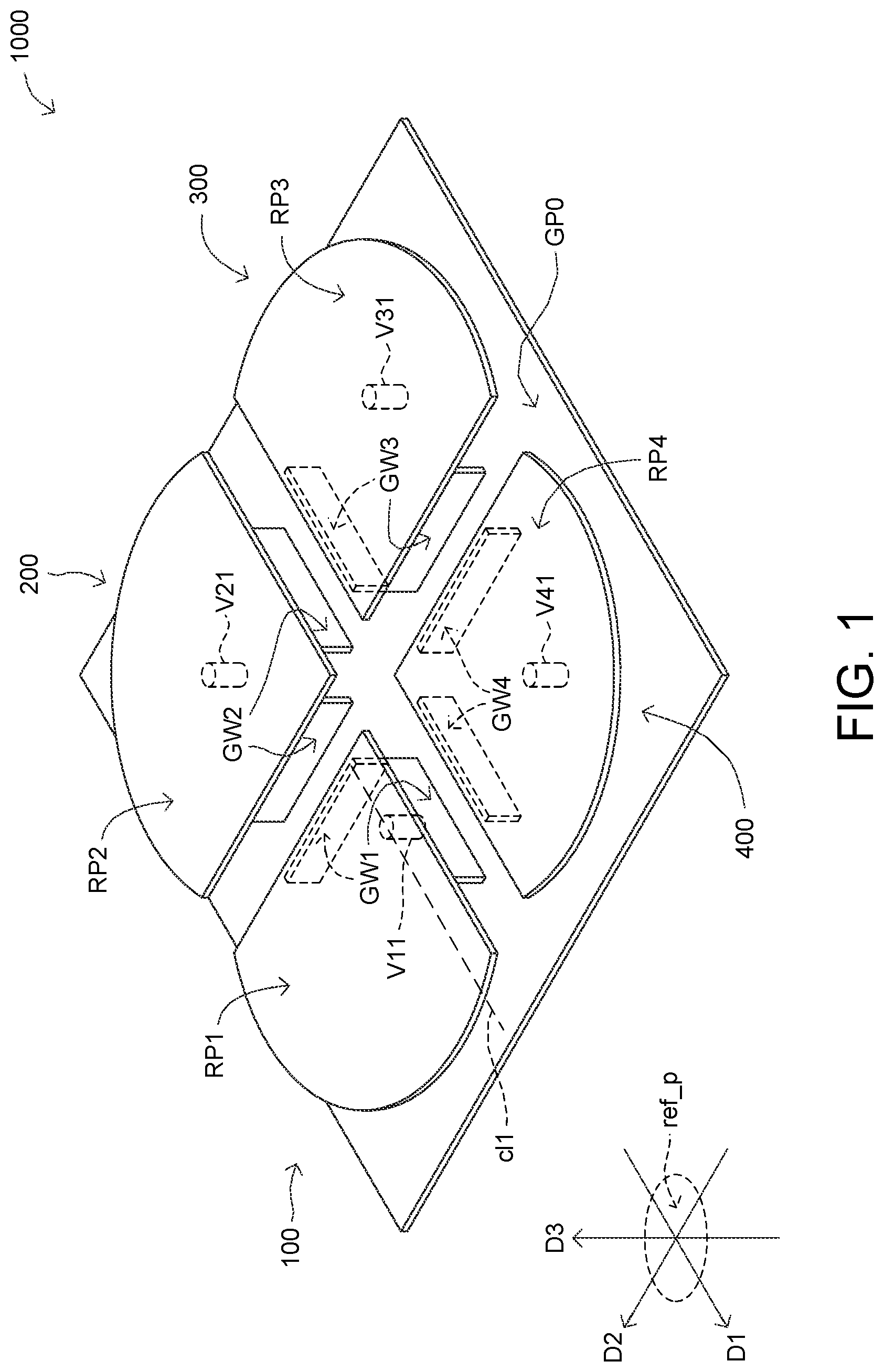
is a schematic diagram illustrating a perspective view of an antenna 1000 according to an example of the present disclosure. Referring to , the antenna 1000 includes a ground plane GP 0 and a plurality of resonating units, for example, four the resonating units 100 , 200 , 300 and 400 . The resonating units 100 - 400 are arranged above the ground plane GP 0 . Each of the resonating units 100 - 400 has a radiating plate and a ground wall. For example, the resonating unit 100 has a radiating plate RP 1 and a ground wall GW 1 . Likewise, the resonating unit 200 has a radiating plate RP 2 and a ground wall GW 2 . Similarly, the resonating unit 300 has a radiating plate RP 3 and a ground wall GW 3 , and the resonating unit 400 has a radiating plate RP 4 and a ground wall GW 4 .
The ground plane GP 0 is arranged as extending along a reference plane ref_p which is defined by a direction D 1 and a direction D 2 . Furthermore, each of the radiating plates RP 1 -RP 4 is arranged as being substantially parallel with the ground plane GP 0 . On the other hand, each of the ground walls GW 1 -GW 4 may have two portions, the ground walls GW 1 -GW 4 are arranged as extending along a direction D 3 , and the direction D 3 is substantially perpendicular to the reference plane ref_p which the ground plane GP 0 extends along. That is, the ground walls GW 1 -GW 4 are substantially perpendicular to the ground plane GP 0 and the radiating plates RP 1 -RP 4 . Moreover, the ground walls GW 1 -GW 4 may connect the ground plane GP 0 the radiating plates RP 1 -RP 4 respectively.
In the resonating unit 100 , the ground wall GW 1 is adapted to connect the radiating plate RP 1 with the ground plane GP 0 . Likewise, in the resonating unit 200 , the ground wall GW 2 is adapted to connect the radiating plate RP 2 with the ground plane GP 0 . Similarly, the ground wall GW 3 of the resonating unit 300 is adapted to connect the radiating plate RP 3 with the ground plane GP 0 , and the ground wall GW 4 of the resonating unit 400 is adapted to connect the radiating plate RP 4 with the ground plane GP 0 .
In operation, the antenna 1000 has an antenna gain for the TX signal or the RX signal. In order to make the antenna gain tunable with respect to different frequency bands, the antenna 1000 further includes connecting elements arranged in the resonating units 100 - 400 respectively. These connecting elements contribute to adjust a corresponding antenna gain at a desired frequency band. For example, the antenna 1000 includes a connecting element, i.e., a via V 11 arranged in the resonating unit 100 . The via V 11 is arranged between the radiating plate RP 1 and the ground plane GP 0 . The via V 11 extends substantially along the direction D 3 , such that the via V 11 is substantially perpendicular to the radiating plate RP 1 and the ground plane GP 0 , and substantially parallel with the ground wall GW 1 .
The via V 11 has a conductive material to convey an electrical signal or a magnetic signal, such that the via V 11 is adapted to couple the radiating plate RP 1 to the ground plane GP 0 . For example, the via V 11 serves to directly connect (e.g., conductively connect) the radiating plate RP 1 with the ground plane GP 0 , or indirectly couple (e.g., electromagnetically couple) the radiating plate RP 1 to the ground plane GP 0 . In one exemplary arrangement, the via V 11 directly contacts both the radiating plate RP 1 and the ground plane GP 0 , such that the radiating plate RP 1 is directly connected with the ground plane GP 0 through the via V 11 .
In another exemplary arrangement, the via V 11 directly contacts one of the radiating plate RP 1 and the ground plane GP 0 , but the via V 11 is indirectly coupled to the other one of the radiating plate RP 1 and the ground plane GP 0 . Therefore, the radiating plate RP 1 is indirectly coupled to the ground plane GP 0 through the via V 11 . In an alternative arrangement, the via V 11 is indirectly coupled to both the radiating plate RP 1 and the ground plane GP 0 , hence the radiating plate RP 1 is indirectly coupled to the ground plane GP 0 through the via V 11 .
Similar to the via V 11 of the resonating unit 100 , other resonating units 200 , 300 and 400 also include corresponding vias V 21 , V 31 and V 41 respectively. For the resonating unit 200 , the via V 21 is arranged between the radiating plate RP 2 and the ground plane GP 0 . The via V 21 is substantially perpendicular to the radiating plate RP 2 and the ground plane GP 0 , and substantially parallel with the ground wall GW 2 . Likewise, the via V 31 of the resonating unit 300 is arranged between the radiating plate RP 3 and the ground plane GP 0 . The via V 31 is substantially perpendicular to the radiating plate RP 3 and the ground plane GP 0 , and substantially parallel with the ground wall GW 3 . Furthermore, the via V 41 of the resonating unit 400 is arranged between the radiating plate RP 4 and the ground plane GP 0 . The via V 41 is substantially perpendicular to the radiating plate RP 4 and the ground plane GP 0 , and substantially parallel with the ground wall GW 4 .
In the example of , each of the resonating units 100 - 400 include one via. In other examples, each of the resonating units 100 - 400 may include two or more vias (not shown in ). The resonating units 100 - 400 may include different amounts of vias, such as, the resonating unit 100 includes one via, and the resonating unit 200 includes three vias, etc.
A is a schematic diagram illustrating a top view of the resonating unit 100 of , and the resonating unit 100 in A is viewed along the direction D 3 . Referring to A , the radiating plate RP 1 extends along another predefined reference plane (not shown) which is parallel with the reference plane ref_p of the ground plane GP 0 , and there are boundaries B 1 , B 2 and B 3 surrounding the radiating plate RP 1 . The via V 11 of the resonating unit 100 has a projection PJ_V 11 ( 1 ). The projection PJ_V 11 ( 1 ) is taken along the direction D 3 and projected on the radiating plate RP 1 . The projection PJ_V 11 ( 1 ) is located within the boundaries B 1 -B 3 .
Furthermore, two portions of the ground wall GW 1 also have projections taken along the direction D 3 and projected on the radiating plate RP 1 . The projections of two portions of the ground wall GW 1 may extend to intersect at a projection position PJ( 0 ), and the projection position PJ( 0 ) may be located around an intersection of the boundaries B 1 and B 2 . In a comparative example (other than the examples of the present disclosure), a via is arranged at the projection position PJ( 0 ) to serve as a part of the ground wall GW 1 . However, the via V 11 of the present disclosure may not serve as any part of the ground wall GW 1 , therefore, the projection PJ_V 11 ( 1 ) of the via V 11 may not be located at the projection position PJ( 0 ).
In addition, the antenna 100 may adjust its antenna gain by changing the location of the via V 11 . For example, when the via V 11 is changed to another location with a projection PJ_V 11 ( 2 ) (which is projected on the radiating plate RP 1 , and does not overlap projection PJ_V 11 ( 1 )), the antenna 1000 may achieve a different value of antenna gain at a desired frequency band.
B illustrates a top view of another exemplary resonating unit 100 b with respect to A . The resonating unit 100 b of B is similar to the resonating unit 100 of A except that, resonating unit 100 b of B further includes two vias V 12 and V 13 . The via V 12 has a projection PJ_V 12 on the radiating plate RP 1 , while the via V 13 has a projection PJ_V 13 on the radiating plate RP 1 . The projections PJ_V 12 and PJ_V 13 may not overlap the projection PJ_V 11 of the via V 11 . Furthermore, the projections PJ_V 11 to PJ_V 13 of the vias V 11 -V 13 may not overlap the projecting position PJ( 0 ) at which the two portions of the ground wall GW 1 intersect. Moreover, at least one of the vias V 11 -V 13 are arranged under the radiating plate RP 1 , such that, at least one of the projections PJ_V 11 to PJ_V 13 of the vias V 11 -V 13 are located within the boundaries B 1 -B 3 of the radiating plate RP 1 .
Since the resonating unit 100 b of B has a different amount of vias (i.e., three) compared to the amount of via (i.e., one) of the resonating unit 100 of A , the antenna 1000 of B may achieve an antenna gain different from that of A .
A- 3 J are schematic diagrams illustrating cross-sectional views of the resonating units 100 - 1 a to 100 - 1 j according to various examples of the present disclosure. The cross-sectional views in A- 3 J are taken along the cutting line cl 1 in , 2 A and 2 B and viewed from the direction D 2 . First, referring to A , the resonating unit 100 - 1 a includes one connecting element, the via V 11 (which may be referred to as “the first connecting element”). The via V 11 is arranged between the radiating plate RP 1 and the ground plane GP 0 .
The via V 11 substantially extends along the direction D 3 , such that the via V 11 is substantially perpendicular to the radiating plate RP 1 and the ground plane GP 0 , and substantially parallel with the ground wall GW 1 . The via V 11 may directly contact one or both of the radiating plate RP 1 and the ground plane GP 0 . Alternatively, the via V 11 may be electromagnetically coupled to one or both of the radiating plate RP 1 and the ground plane GP 0 . In the example of A , via V 11 directly contacts both of the radiating plate RP 1 and the ground plane GP 0 .
More particularly, via V 11 has one end 11 and another end 12 . The end 11 of the via V 11 directly contacts a lower surface of the radiating plate RP 1 , and the end 12 of the via V 11 directly contacts an upper surface of the ground plane GP 0 . In this arrangement, the via V 11 is conductively connected with both the radiating plate RP 1 and the ground plane GP 0 , such that the via V 11 serves to conductively connect the radiating plate RP 1 with the ground plane GP 0 .
Next, referring to B , the resonating unit 100 - 1 b is similar to the resonating unit 100 - 1 a of A except that, the via V 11 of resonating unit 100 - 1 b directly contacts the ground plane GP 0 but may not directly contact the radiating plate RP 1 .
For example, the end 11 of the via V 11 may not directly contact the radiating plate RP 1 . Instead, the end 11 of the via V 11 is connected with a pad pd 1 , and the pad pd 1 is isolated from the radiating plate RP 1 . The pad pd 1 has a conductive material, such that an electrical signal or a magnetic signal may be transmitted through the pad pd 1 . Therefore, the via V 11 may be electromagnetically coupled to the radiating plate RP 1 through the pad pd 1 . In this arrangement, the via V 11 serves to electromagnetically couple the ground plane GP 0 to the radiating plate RP 1 .
Next, referring to C , the resonating unit 100 - 1 c is similar to the resonating unit 100 - 1 a of A except that, the via V 11 of resonating unit 100 - 1 b directly contacts the radiating plate RP 1 but may not directly contact the ground plane GP 0 .
For example, the end 12 of the via V 11 may not directly contact the ground plane GP 0 . Instead, the end 12 of the via V 11 is connected with a pad pd 2 , and the pad pd 2 is isolated from the ground plane GP 0 . The pad pd 2 is similar to the pad pd 1 , and pad pd 2 may serves to convey an electrical signal or a magnetic signal. Therefore, the via V 11 may be electromagnetically coupled to the ground plane GP 0 through the pad pd 2 .
Next, referring to D , the resonating unit 100 - 1 d is similar to the resonating unit 100 - 1 c of C except that, the via V 11 of resonating unit 100 - 1 b is electromagnetically coupled to both the radiating plate RP 1 and the ground plane GP 0 . For example, the end 11 of the via V 11 is connected with a pad pd 1 , which is isolated from the radiating plate RP 1 . In this arrangement, the via V 11 may be electromagnetically coupled to the radiating plate RP 1 through the pad pd 1 and electromagnetically coupled to the ground plane GP 0 through the pad pd 2 .
Next, referring to E , the resonating unit 100 - 1 e is similar to the resonating unit 100 - 1 c of C except that, the via V 11 of the resonating unit 100 - 1 e has a portion protruding from the upper surface of the radiating plate RP 1 . More particularly, the via V 11 includes one portion V 11 a and another portion V 11 b . The portion V 11 a is arranged between the radiating plate RP 1 and the ground plane GP 0 , and the portion V 11 b is arranged above the portion V 11 a . Furthermore, the portion V 11 b is arranged above the radiating plate RP 1 , such that the portion V 11 b may protrude from the upper surface of the radiating plate RP 1 .
One end of the portion V 11 a is connected with a pad pd 2 , and another end of the portion V 11 a directly contacts the lower surface of the radiating plate RP 1 . On the other hand, one end of the portion V 11 b is connected with a pad pd 1 , and another end of the portion V 11 b directly contacts the upper surface of the radiating plate RP 1 .
Next, referring to F , the resonating unit 100 - 1 f is similar to the resonating unit 100 - 1 c of C except that, the resonating unit 100 - 1 f of F further includes a trace t 1 . The trace t 1 has a conductive material, which may convey an electrical signal or a magnetic signal. The trace t 1 is arranged as being substantially parallel with the radiating plate RP 1 and the ground plane GP 0 , and substantially perpendicular to the via V 11 and the ground wall GW 1 .
One end of the trace t 1 directly contacts the ground wall GW 1 . Another end of the trace t 1 is arranged under the pad pd 2 and isolated from the pad pd 2 , such that the trace t 1 may be electromagnetically coupled to the pad pd 2 , and then coupled to the via V 11 . In this arrangement, the via V 11 is electromagnetically coupled to the ground wall GW 1 through pad pd 2 and the trace t 1 .
Next, referring to G , the resonating unit 100 - 1 g is similar to the resonating unit 100 - 1 f of F except that, the pad pd 2 of the resonating unit 100 - 1 g directly contacts the trace t 1 . Furthermore, the via V 11 directly contacts the pad pd 2 . More particularly, the via V 11 has two portions. One portion V 11 b of via V 11 is arranged between the radiating plate RP 1 and the pad pd 2 , while another portion V 11 a of via V 11 is arranged between the pad pd 2 and another pad pd 1 . The via V 11 may be electromagnetically coupled to the ground plane GP 0 through the pad pd 1 . In this arrangement, the via V 11 serves to conductively connect the radiating plate RP 1 with the ground wall GW 1 , and serves to electromagnetically couple the radiating plate RP 1 to the ground plane GP 0 .
Next, referring to H , the resonating unit 100 - 1 h is similar to the resonating unit 100 - 1 g of G except that, the resonating unit 100 - 1 h further includes another pad pd 3 and another trace t 2 . The pad pd 3 directly contacts the trace t 2 . The V 11 is coupled to the ground wall GW 1 through the trace t 2 .
The via V 11 of resonating unit 100 - 1 h has three portions V 11 a , V 11 b and V 11 c . The portion V 11 b is arranged above the portion V 11 a , and the portion V 11 c is arranged above the portion V 11 b . Furthermore, the portion Vila is arranged between the pads pd 2 and pad 1 , the portion V 11 b is arranged between the pads pd 1 and pd 3 , and the portion V 11 c is arranged between the pad pd 3 and the lower surface of the radiating plate RP 1 . The via V 11 may be conductively connected with the ground wall GW 1 through a conductive path formed by the pad pd 1 and the trace t 1 , and through another conductive path formed by the pad pd 3 and the trace t 2 .
Next, referring to I , the resonating unit 100 - 1 i is similar to the resonating unit 100 - 1 f of F except that, the via V 11 of the resonating unit 100 - 1 i is directly connected with the trace t 1 , without connecting with the pad pd 2 . The via V 11 may be conductively connected with the ground wall GW 1 through the trace t 1 .
Next, referring to J , the resonating unit 100 - 1 j includes two vias V 11 and V 12 . The via V 11 may be referred to as “the first connecting element”, and the via V 12 may be referred to as “the second connecting element”. The via V 11 is connected with the via V 12 through the trace t 1 . The trace t 1 has one end e_ 1 connected with the via V 12 and another end e_ 2 connected with the via V 11 . The via V 11 is arranged between the end e_ 2 of the trace t 1 and the upper surface of the ground plane GP 0 , while the via V 12 is arranged between the end e_ 1 of the trace t 1 and the lower surface of the radiating plate RP 1 . In this arrangement, the radiating plate RP 1 may be conductively connected with the ground plane GP 0 through the via V 12 , the trace t 1 and the via V 11 .
The via V 11 is substantially parallel with the via V 12 , but the via V 11 may not be aligned with the via V 12 at the same vertical line along the direction D 3 . More particularly, the via V 11 has a projection PJ_V 11 . The projection PJ_V 11 is taken along the direction D 3 and projected on the predefined reference plane which the radiating plate RP 1 extends along. Furthermore, the via V 12 has a projection PJ_V 12 , which is taken along the direction D 3 and projected on the radiating plate RP 1 . The projection PJ_V 11 of the via V 11 may not overlap the projection PJ_V 12 of the via V 12 . In the example of J , projection PJ_V 12 of the via V 12 is located within the boundaries B 1 , B 2 and B 3 of the radiating plate RP 1 (the boundaries B 1 , B 2 and B 3 of the radiating plate RP 1 are shown in A and 2 B ). In contrast, the projection PJ_V 11 of the via V 11 may be located outside the boundaries B 1 , B 2 and B 3 of the radiating plate RP 1 .
A and 4 B are schematic diagrams illustrating cross-sectional views of the resonating units 100 - 2 a and 100 - 2 b according to other examples of the present disclosure. First, referring to A , the resonating unit 100 - 2 a is similar to the resonating unit 100 - 1 c of C except that, the resonating unit 100 - 2 a further includes a trace t 1 and a control element. The via V 11 is coupled to the trace t 1 through the control element. The control element is e.g., a filter f 1 . The filter f 1 is arranged between the pad pd 2 and the trace t 1 , such that the filter f 1 may conductively connect the via V 11 with the ground wall GW 1 through the pad pd 2 and the trace t 1 .
In operation, the filter f 1 serves to selectively transmit signals of interest at a desired frequency band, and the filter f 1 bypass unwanted signals at other frequency band. Therefore, antenna gain of the antenna 1000 may be adjusted for different frequency bands respectively.
In other examples, the control element of the resonating unit 100 - 2 a may be a diode, a switch or an impedance tuner (not shown in A ).
Next, referring to B , the resonating unit 100 - 2 b is similar to the resonating unit 100 - 2 a of A except that, the resonating unit 100 - 2 b includes two control elements, i.e., two diodes d 1 and d 2 . Furthermore, the resonating unit 100 - 2 b further includes another trace t 2 and another pad pd 1 . The diode d 2 , which replaces the filter f 1 of A , is connected with pad pd 2 and the trace t 1 . On the other hand, the pad pd 1 is arranged between two portions V 11 a and V 11 b of via V 11 , and another diode d 1 is connected with pad pd 1 and the trace t 2 .
The via 11 is selectively connected with the ground wall GW 1 through the pad pd 1 , the diode d 1 and the trace t 2 , according to a status of the diode d 1 . When the diode d 1 operates at a forward bias, the conductive path between the pad pd 1 and the trace t 2 is turned on (i.e., short circuit), such that the via V 11 may be conductively connected with the ground wall GW 1 . Furthermore, the via 11 may be also conductively connected with the ground wall GW 1 through the pad pd 2 , the diode d 2 and the trace t 1 , when the diode d 2 operates at a forward bias. On the other hand, the via V 11 is still electromagnetically coupled to the ground plane GP 0 through the pad pd 2 . In this arrangement, antenna gain of the antenna 1000 may be adjusted according to the status of the diodes d 1 and d 2 .
In other examples, each of the two control elements of the resonating unit 100 - 2 b may be a filter, a switch or an impedance tuner (not shown in B ).
A- 5 H are schematic diagrams illustrating cross-sectional views of the resonating units 100 - 3 a to 100 - 3 h according to still other examples of the present disclosure. First, referring to A , the resonating unit 100 - 3 a is similar to the resonating unit 100 - 2 a of A except that, the control element of the resonating unit 100 - 3 a is a switch s 1 , which replaces the filter f 1 of the resonating unit 100 - 2 a . Furthermore, the resonating unit 100 - 3 a further includes another via V 12 (i.e., the second connecting element). The via V 12 serves to conductively connect the radiating plate RP 1 with the ground wall GW 1 through the trace t 1 . In addition, the via V 11 is connected with the pad pd 1 , and the via V 12 is connected with a pad pd 2 , and the switch s 1 is connected with the pad pd 1 and the pad pd 2 . Then, the via V 11 is coupled to the via V 12 through the switch s 1 .
Both the vias V 11 and V 12 are arranged under the radiating plate RP 1 . The via V 12 is arranged as being substantially parallel with the via V 11 , and the via V 12 may not be aligned with the via V 11 at the same vertical line along the third direction D 3 . The projection PJ_V 11 of the via V 11 , which is projected on the radiating plate RP 1 , may not overlap the projection PJ_V 12 of the via V 12 . In the example of A , both the projection PJ_V 11 of the via V 11 and the projection PJ_V 12 of the via V 12 are located within the boundaries B 1 , B 2 and B 3 of the radiating plate RP 1 (the boundaries B 1 , B 2 and B 3 of the radiating plate RP 1 are shown in A and 2 B ).
In operation, the switch s 1 serves to selectively connect the via V 11 with the via V 12 , depending on the status of the switch s 1 . When the switch s 1 is turned on (i.e., short circuit), the via V 11 may be connected with the via V 12 , and further connected with the ground wall GW 1 through the trace t 1 .
In another example, the resonating unit 100 - 3 a may include another via V 13 (not shown in A ), and the switch s 1 may selectively connect the via V 11 with the via V 13 . That is, the resonating unit 100 - 3 a includes two conductive paths, the first path is formed by via V 11 , switch s 1 and via V 12 , while the second path is formed by via V 11 , switch s 1 and via V 13 . The switch s 1 functions to conduct one of the first path and the second path.
Next, referring to B , the resonating unit 100 - 3 b is similar to the resonating unit 100 - 3 a of A except that, each of the vias V 11 and V 12 has two portions. The via V 11 has one portion V 11 a and another portion V 11 b . The portion V 11 a is arranged between the pad pd 1 and ground plane GP 0 , and the portion V 11 b is arranged above the portion V 11 a , the portions V 11 b and Vila are coupled to each other through the pad pd 1 . Likewise, the via V 12 has one portion V 12 a and another portion V 12 b . The portion V 12 a is arranged between the pad pd 2 and ground plane GP 0 , and the portion V 12 b is arranged above the portion V 12 a , the portions V 12 b and V 12 a are coupled to each other through the pad pd 2 . The radiating plate RP 1 is conductively connected with the ground plane GP 0 through the portions V 11 a and V 11 b and pad pd 1 . Likewise, the radiating plate RP 1 is also conductively connected with the ground plane GP 0 through the portions V 12 a and V 12 b and pad pd 2 .
Unlike the via V 12 of A which is coupled to the ground wall GW 1 through the trace t 1 , the via V 12 of B may not be coupled to the ground wall GW 1 (i.e., the resonating unit 100 - 3 b of B may not include the trace t 1 as the resonating unit 100 - 3 a of A ).
Next, referring to C , the resonating unit 100 - 3 c is similar to the resonating unit 100 - 3 b of B except that, the via V 12 of the resonating unit 100 - 3 c has one portion, and the via V 12 may not directly contact the ground plane GP 0 . Instead, the via V 12 is electromagnetically coupled to the ground plane GP 0 through the pad pd 2 .
Next, referring to D , the resonating unit 100 - 3 d is similar to the resonating unit 100 - 3 b of B except that, each of the vias V 11 and V 12 of the resonating unit 100 - 3 d has one portion. The via V 11 may not directly contact the ground plane GP 0 , and instead, the via V 11 is electromagnetically coupled to the ground plane GP 0 through the pad pd 1 . Likewise, the via V 12 may not directly contact the radiating plate RP 1 , but is electromagnetically coupled to the radiating plate RP 1 through the pad pd 2 .
Next, referring to E , the resonating unit 100 - 3 e is similar to the resonating unit 100 - 3 a of A except that, the switch s 1 of the resonating unit 100 - 3 e is arranged on the upper surface of the radiating plate RP 1 . In one example, the vias V 11 and V 12 may penetrate the radiating plate RP 1 , such that the switch s 1 may be connected with the vias V 11 and V 12 through wires wr 11 and wr 12 respectively. In another example (not shown in E ), the vias V 11 and V 12 may not penetrate the radiating plate RP 1 , instead, the wires wr 11 and wr 12 may penetrate the radiating plate RP 1 to arrive the vias V 11 and V 12 respectively.
In other examples of A- 5 F , the control element of the resonating unit 100 - 3 a to 100 - 3 e may be a diode, a filter or an impedance tuner (not shown in A- 5 F ).
Next, referring to F , the resonating unit 100 - 3 f is similar to the resonating unit 100 - 3 e of E except that, the resonating unit 100 - 3 f includes two control elements, i.e., the switch s 1 and the diode d 1 . The switch s 1 may be referred to as “the first control element”, and the diode d 1 may be referred to as “the second control element”. The diode d 1 is adapted to couple the via V 11 to the via V 12 . The diode d 1 connects the pad pd 1 with the trace t 1 , therefore, the diode d 1 is also adapted to couple the first connecting element V 11 to the ground wall GW 1 through the trace t 1 .
In other examples, the first control element of the resonating unit 100 - 3 f may be a diode, a filter or an impedance tuner. Furthermore, the second control element of the resonating unit 100 - 3 f may be a switch, a filter or an impedance tuner (not shown in F ).
Next, referring to G , the resonating unit 100 - 3 g is similar to the resonating unit 100 - 3 b of B except that, the via V 11 of the resonating unit 100 - 3 g is connected with the via V 12 through a switch s 1 arranged on a bottom circuit board BC of the antenna 1000 . The bottom circuit board BC is, e.g., a circuit board carrying peripheral components of the antenna 1000 . In one example, the bottom circuit board BC is arranged under the ground plane GP 0 , and the switch s 1 may be arranged on a lower surface of the bottom circuit board BC. The ground plane GP 0 may have through holes to allow the vias V 11 and V 12 to penetrate. Therefore, the vias V 11 and V 12 may pass through the ground plane GP 0 to arrive and coupled to the bottom circuit board BC, and then to connect with the switch s 1 . Furthermore, the via V 12 is connected with the ground wall GW 1 through the trace t 1 .
The via V 11 has two portions V 11 a and V 11 b . The portion V 11 a may be electromagnetically coupled to the ground plane GP 0 around one through hole of the ground plane GP 0 . Likewise, one portion V 12 a may be electromagnetically coupled to the ground plane GP 0 around another through hole of the ground plane GP 0 .
Next, referring to H , the resonating unit 100 - 3 h is similar to the resonating unit 100 - 3 g of G except that, the resonating unit 100 - 3 h further includes two connecting elements, i.e., a via V 13 and a via V 14 . Unlike the vias V 11 and V 12 which are arranged between the radiating plate RP 1 and the bottom circuit board BC, on the other hand, at least one of the vias V 13 and V 14 are arranged between the ground plane GP 0 and the bottom circuit board BC. Furthermore, the vias V 13 and V 14 may not be connected with any pads, in contrast, the via V 11 is connected with the pad pd 1 , and the via V 12 is connected with the pad pd 2 .
More particularly, the vias V 11 , V 12 , V 13 and V 14 are substantially parallel with one another, but the vias V 11 , V 12 , V 13 and V 14 may not be aligned with one another at the same vertical line along the direction D 3 . More particularly, the vias V 11 , V 12 , V 13 and V 14 have respective projections PJ_V 11 , PJ_V 12 , PJ_V 13 and PJ_V 14 . For the vias V 11 , V 12 and V 14 , their projections PJ_V 11 , PJ_V 12 and PJ_V 14 are projected on the radiating plate RP 1 . On the other hand, for the via V 13 , its projection PJ_V 13 is projected on a predefined reference plane which the radiating plate RP 1 extends along. The projections PJ_V 11 , PJ_V 12 , PJ_V 13 and PJ_V 14 may not overlap one another.
In the example of H , the vias V 11 , V 12 and V 14 are arranged under the radiating plate RP 1 , such that the projections PJ_V 11 , PJ_V 12 and PJ_V 14 may fall within the boundaries B 1 , B 2 and B 3 of the radiating plate RP 1 (the boundaries B 1 , B 2 and B 3 of the radiating plate RP 1 are shown in A and 2 B ). On the other hand, the projection PJ_V 13 of the via V 13 may be located outside the boundaries B 1 , B 2 and B 3 of the radiating plate RP 1 .
In operation, the switch s 1 serves to selectively connect the vias V 11 , V 12 , V 13 and V 14 with one another. Depending on a routing scheme of the switch s 1 , one of the vias V 11 -V 14 may be connected with other one or more of the vias V 11 -V 14 . Such as, the via V 13 may be connected with the neighboring via V 11 . In another example, the via V 13 may be connected with two vias V 11 and V 12 .
In other examples of G and 5 H , the switch s 1 of the resonating unit 100 - 3 g and 100 - 3 h may be replaced by a diode, a filter or an impedance tuner (not shown in G and 5 H ).
A and 6 B are schematic diagrams illustrating cross-sectional views of the resonating units 100 - 4 a and 100 - 4 b according to yet other examples of the present disclosure. First, referring to A , the resonating unit 100 - 4 a is similar to the resonating unit 100 - 3 g of G except that, the control element of the resonating unit 100 - 4 a is an impedance tuner it 1 , which replaces the switch s 1 of G . Furthermore, the via V 12 of the resonating unit 100 - 4 a is arranged between the ground plane GP 0 and the bottom circuit board BC, and the via V 12 may not penetrating the ground plane GP 0 . Moreover, the via V 11 is electromagnetically coupled to the radiating plate RP 1 through the pad pd 1 , but via V 11 may not directly contact the ground wall GW 1 and the radiating plate RP 1 . In operation, the impedance tuner it 1 serves to adjust impedance of a conductive path formed by the via V 11 and the via V 12 , and the antenna 1000 may achieve different values of antenna gain according to different values of adjusted impedance.
In other examples, the control element of the resonating unit 100 - 4 a may be a diode, a filter or a switch (not shown in A ).
Next, referring to B , the resonating unit 100 - 4 b is similar to the resonating unit 100 - 4 a of A except that, the resonating unit 100 - 4 b further includes another connecting element (i.e., the via V 13 ) and another control element (i.e., the diode d 1 ). The via V 13 is connected with the via V 11 through the pad pd 2 , the diode d 1 and the pad pd 1 . Therefore, the radiating plate RP 1 may be conductively connected with the bottom circuit board BC through the vias V 13 and V 11 , depending on the status of the diode d 1 .
In other examples, the impedance tuner it 1 of the resonating unit 100 - 4 b may be replaced by a diode, a filter or a switch. Furthermore, the diode d 1 of the resonating unit 100 - 4 b may be replaced by a filter, a switch or an impedance tuner (not shown in B ).
It will be apparent to those skilled in the art that various modifications and variations can be made to the disclosed embodiments. It is intended that the specification and examples be considered as exemplary only, with a true scope of the disclosure being indicated by the following claims and their equivalents.
Figures (14)
Citations
This patent cites (6)
- US6914563
- US8223077
- US10833401
- US11289809
- US2021/0013610
- USWO-2021088630