Semiconductor Device with Buried Gate Word Line Drivers
Abstract
A semiconductor device includes a substrate; and a plurality of sub-word line drivers, each of the sub-word line drivers including a plurality of transistors, wherein at least one of the plurality of transistors has a buried gate structure positioned in the substrate.
Claims (18)
1. A semiconductor device, comprising: a substrate; and a plurality of sub-word line drivers, each of the sub-word line drivers including a plurality of transistors, wherein at least one of the plurality of the transistors has a buried gate structure positioned in the substrate, wherein the transistors include: a NMOS transistor having a buried gate structure; and a PMOS transistor having a planar gate structure formed over the substrate.
9. A semiconductor device, comprising: a substrate including a cell region and a sub-word line driver region; a plurality of cell word lines extending along a first direction in the substrate of the cell region and spaced apart from each other along a second direction which is perpendicular to the first direction; and a plurality of main word lines extending along the first direction in the substrate of the sub-word line driver region and spaced apart from each other along the second direction, wherein each of the plurality of the main word lines constitutes a plurality of transistors, and at least one of the plurality of the transistors includes a buried gate structure positioned in the substrate, wherein the transistors include: a first NMOS transistor having a buried gate structure; and a PMOS transistor having a planar gate structure formed over the substrate.
Show 16 dependent claims
2. The semiconductor device of claim 1 , wherein an upper surface of the buried gate structure is positioned at the same level as an upper surface of the substrate.
3. The semiconductor device of claim 1 , wherein a lower surface of the buried gate structure is positioned at a lower level than an upper surface of the substrate.
4. The semiconductor device of claim 1 , wherein the plurality of the transistors include: a PMOS transistor and first and second NMOS transistors.
5. The semiconductor device of claim 1 , wherein a line width of the PMOS transistor is greater than a line width of the first NMOS transistor.
6. The semiconductor device of claim 1 , wherein the first NMOS transistor and the PMOS transistor are electrically connected through a contact.
7. The semiconductor device of claim 1 , wherein a line width of the PMOS transistor is greater than a line width of the NMOS transistor.
8. The semiconductor device of claim 1 , wherein the NMOS transistor and the PMOS transistor are electrically connected through a contact.
10. The semiconductor device of claim 9 , wherein an upper surface of the buried gate structure is positioned at the same level as an upper surface of the substrate.
11. The semiconductor device of claim 9 , wherein a lower surface of the buried gate structure is positioned at a lower level than an upper surface of the substrate.
12. The semiconductor device of claim 9 , wherein the transistors constituted by each of the main word lines are arranged side by side along a first direction and electrically connected to each other.
13. The semiconductor device of claim 9 , further comprising: a second NMOS transistor between the main word lines that are positioned adjacent to each other along a second direction.
14. The semiconductor device of claim 13 , wherein the second NMOS transistor includes a ‘C’-shaped buried gate structure.
15. The semiconductor device of claim 13 , wherein the second NMOS transistor includes an island-shaped planar gate structure.
16. The semiconductor device of claim 9 , wherein the cell region and the sub-word line driver region are positioned adjacent to each other along the first direction.
17. The semiconductor device of claim 9 , wherein the sub-word line driver region is positioned between the neighboring cell regions.
18. The semiconductor device of claim 9 , wherein the cell word line includes a buried gate structure.
Full Description
Show full text →
CROSS-REFERENCE TO RELATED APPLICATIONS
The present application claims priority of Korean Patent Application No. 10-2021-0085650, filed on Jun. 30, 2021, which is incorporated herein by reference in its entirety.
BACKGROUND
1. Field
Various embodiments of the present invention relate generally to a semiconductor device and, more particularly, to a semiconductor device including a sub-word line driver region and a fabricating method thereof.
2. Description of the Related Art
Typically, a semiconductor device may be divided into a cell region including a plurality of memory cells and a peripheral circuit region for controlling the operation of the memory cells of the cell region. The peripheral circuit region may typically include a sense amplifier (SA) region and a sub-word line driver region.
As the size of semiconductor devices is reduced, the length of a gate channel of the peripheral circuit region is also reduced which may result in deteriorating transistor characteristics.
SUMMARY
Embodiments of the present invention are directed to a semiconductor device and a method for fabricating the semiconductor device. The semiconductor device is capable of securing the gate channel length in a sub-word line driver region
In accordance with an embodiment of the present invention, a semiconductor device includes: a substrate; and a plurality of sub-word line drivers, each of the sub-word line drivers including a plurality of transistors, wherein at least one of the plurality of transistors has a buried gate structure positioned in the substrate.
In accordance with another embodiment of the present invention, a semiconductor device includes: a substrate including a cell region and a sub-word line driver region; a plurality of cell word lines extending along a first direction in the substrate of the cell region and spaced apart from each other along a second direction which is perpendicular to the first direction; and a plurality of main word lines extending along the first direction in the substrate of the sub-word line driver region and spaced apart from each other along the second direction, wherein each of the plurality of the main word lines constitutes a plurality of transistors, and at least one of the plurality of the transistors includes a buried gate structure positioned in the substrate.
In accordance with yet another embodiment of the present invention, a method for fabricating a semiconductor device includes: providing a substrate including a cell region and a sub-word line driver region; forming a plurality of line-type first mask patterns extending along a first direction and spaced apart from each other along a second direction which is perpendicular to the first direction over the substrate of the cell region and the sub-word line driver region; forming a second mask pattern partially covering the first mask pattern; forming a gate trench in the substrate by using the first and second mask patterns; and forming a buried gate structure that gap-fills the gate trench.
These and other features and advantages of the present invention will become understood by those with ordinary skill in the art of the invention from the following drawings and detailed description.
BRIEF DESCRIPTION OF THE DRAWINGS
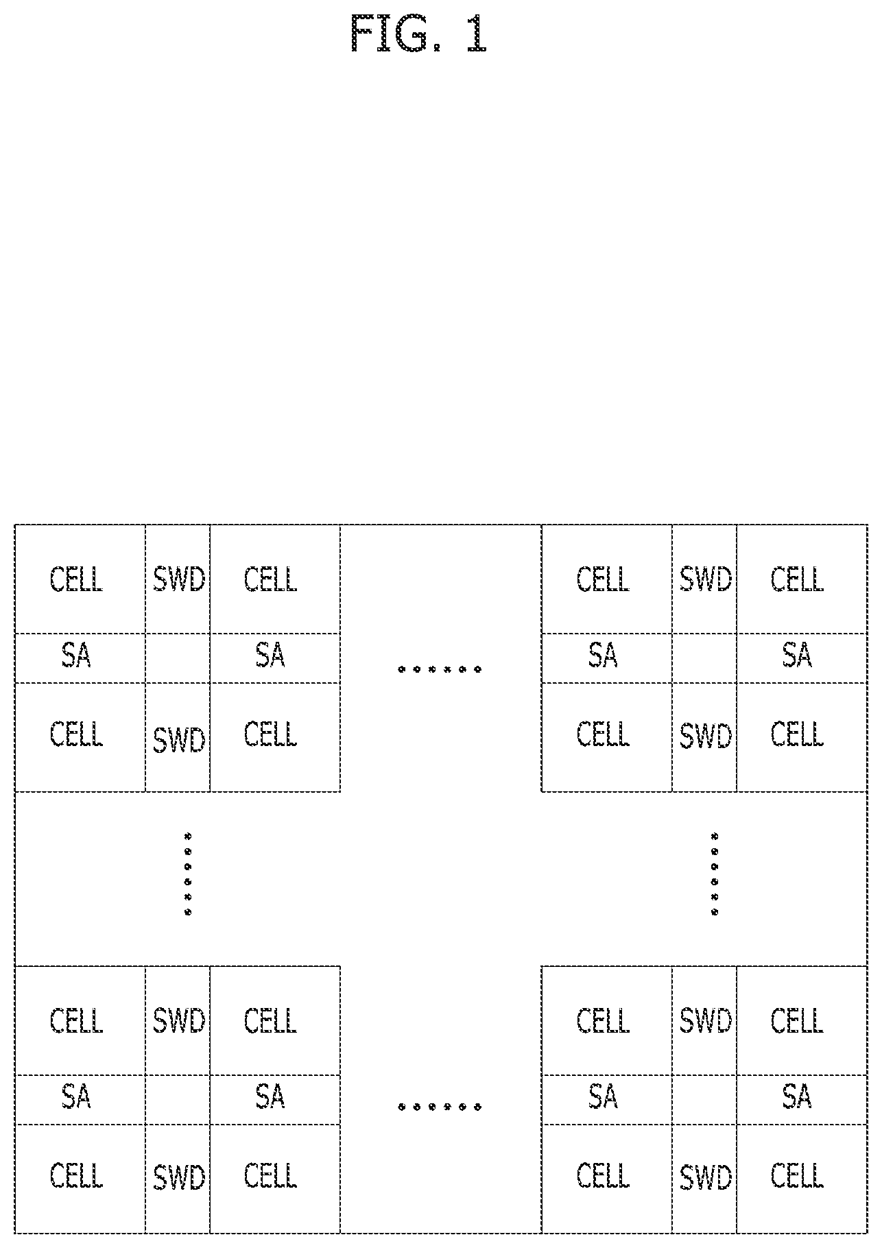
shows an arrangement relationship between a cell mat (CELL) region and a sub-word line driver (SWD) region.
A and 2 B are circuit diagrams illustrating a structure of a general sub-word line driver.
is a layout diagram illustrating a sub-word line driver region in accordance with an embodiment of the present invention.
is a plan view illustrating a semiconductor device in accordance with an embodiment of the present invention.
A and 5 B are plan views illustrating a method of forming a buried gate trench in accordance with an embodiment of the present invention.
A to 6 H are cross-sectional views illustrating a method for fabricating a semiconductor device in accordance with an embodiment of the present invention.
DETAILED DESCRIPTION
Various embodiments of the present invention will be described below in more detail with reference to the accompanying drawings. The present invention may, however, be embodied in different forms and should not be construed as limited to the embodiments set forth herein. Rather, these embodiments are provided so that this disclosure is thorough and complete, and fully conveys the scope of the present invention to those skilled in the art. Throughout the disclosure, like reference numerals refer to like parts throughout the various figures and embodiments of the present invention.
The drawings are not necessarily to scale and, in some instances, proportions may have been exaggerated in order to clearly illustrate features of the embodiments. When a first layer is referred to as being “on” a second layer or “on” a substrate, it not only refers to a case where the first layer is formed directly on the second layer or the substrate but also a case where a third layer exists between the first layer and the second layer or the substrate.
Hereinafter, the various embodiments of the present invention will be described in detail with reference to the attached drawings.
shows an arrangement relationship between a cell mat (CELL) region and a sub-word line driver (SWD) region.
Referring to , a plurality of cell mats CELL may be arranged in a vertical direction and a horizontal direction. Each cell mat CELL may include array-shaped memory cells for storing data.
A sub-word line driver SWD may be disposed between two neighboring cell mats CELL that are disposed adjacent to each other in the horizontal direction. The sub-word line driver SWD may drive a sub-word line in response to a signal which is input through a main word line (MWL) and an output signal of a word line enable driver (PXi Driver).
Each sub-word line driver SWD may operate the word lines (WL) of two neighboring cell mats CELL positioned on the left and right of the sub-word line driver SWD.
Also, a sense amplifier SA may be disposed between the two neighboring cell mats CELL that are disposed in the vertical direction. The sense amplifiers may serve to sense and amplify the data of a bit line in a corresponding cell array. In other words, the sense amplifier may sense and amplify the data of a selected memory cell.
A and 2 B are circuit diagrams illustrating a structure of a general sub-word line driver.
Referring to A , the sub-word line driver may be formed in a sub-word line driver array which respectively outputs the sub-word line drive signals SWL 0 to SWL 3 and SWL 4 to SWL 7 in response to main word line drive signals MWLB 0 and MWLB 1 and word line selection signals PX 0 , PX 2 , PX 4 , and PX 6 . In this case, each sub-word line driver may have the same structure except for input and output signals.
Representatively, the structure of each sub-word line driver will be described with reference to B as follows.
The sub-word line driver may include a PMOS transistor MP 0 and a first NMOS transistor MN 0 . Also, the sub-word line driver may include a second NMOS transistor MN 1 that is coupled to a word line SWL.
The PMOS transistor MP 0 functioning as a pull-up transistor may drive a corresponding word line in response to a main word line driving signal MWLB and a sub-word line driving signal PXID.
In the first NMOS transistor MN 0 functioning as a pull-down transistor, a drain-source channel may be coupled between a back bias voltage VBBW (or a ground voltage VSS) and the drain of the PMOS transistor MP 0 . The main word line driving signal MWLB may be received at a gate of the first NMOS transistor MN 0 .
The second NMOS transistor MN 1 function is for keeping a word line at a ground level when the word line is not selected. In the second NMOS transistor MN 1 a drain-source channel may be coupled between a back bias voltage VBBW (or the ground voltage VSS) and the sub-word line SWL coupled to the drain of the PMOS transistor. An inverted sub-word line driving signal PXIB may be received at the gate of the second NMOS transistor MN 1 .
In B , the pull-up driver of the sub-word line driver SWD is formed of a PMOS transistor, but it may also be formed of an NMOS transistor depending on the type of the sub-word line driver SWD. The second NMOS transistor MN 1 may serve to keep the sub-word line SWL at a ground level when a neighboring word line is enabled. When the second NMOS transistor MN 1 is removed, the first NMOS transistor MN 0 may partially function to keep the sub-word line SWL at the ground level.
B shows an example of a PMOS sub-word line driver. The sub-word line driver SWD may not be limited thereto and may also be realized as an NMOS sub-word line driver.
is a layout diagram illustrating a sub-word line driver region in accordance with an embodiment of the present invention.
Referring to , the sub-word line driver may include a PMOS region and an NMOS region. Herein, the PMOS region may indicate a region in which a PMOS transistor is formed, and the NMOS region may indicate a region in which an NMOS transistor is formed. In other words, gates formed in the PMOS region may constitute PMOS transistors, and gates formed in the NMOS region may constitute NMOS transistors. A plurality of active regions 100 and 110 may be disposed in each of the PMOS region and the NMOS region, respectively. Two main word lines MWL 1 and MWL 2 may be passing through the active regions 100 and 110 . The two main word lines MWL 1 and MWL 2 may include a gate line 120 and 130 , respectively. The sub-word line driver may extend along a first direction D 1 and may include the first and second gate lines 120 and 130 that are spaced apart from each other along a second direction D 2 which is perpendicular to the first direction D 1 .
Also, on both sides of each of the first and second gate lines 120 and 130 , first metal contacts C 1 to C 8 to be coupled to a sub-word line (SWL of B ) and second metal contacts PX 0 , PX 2 , PX 4 , and PX 6 for receiving a sub-word line driving signal (PXID of B ) may be disposed.
In the PMOS region and the NMOS region, the same first metal contact among the first metal contacts C 1 to C 8 may be connected to the same sub-word line (SWL of B ). For example, with referring to B , the first metal contact C 1 may indicate a common node of the PMOS transistor MP 0 and the first NMOS transistor MN 0 connected to sub-word line SWL.
The active regions 100 of the PMOS region may extend along the second direction D 2 and may be spaced apart from each other along the first direction D 1 . The active regions 100 of the PMOS region may have a bar shape.
The active regions 110 of the NMOS region may be formed in an ‘H’ shape. However, the technical concept and spirit of the present embodiment are not limited thereto.
In the PMOS region, first metal contacts C 1 to C 8 and second metal contacts PX 0 , PX 2 , PX 4 and PX 6 may be formed between the first gate line 120 and the second gate line 130 . Among them, the second metal contacts PX 0 , PX 2 , PX 4 , and PX 6 may be disposed in the middle of the active region 100 of the PMOS region. The second metal contacts PX 0 , PX 2 , PX 4 , and PX 6 may be disposed between the first gate line 120 and the second gate line 130 . The first metal contacts C 1 to C 8 may be spaced apart from the second metal contacts PX 0 , PX 2 , PX 4 , and PX 6 . Each one of the second metal contacts may be aligned with two of the first metal contacts in the second direction D 2 and disposed between the two of the first metal contacts. For, example, the second metal contact PX 6 is aligned with the C 4 and C 8 first metal contacts and disposed between the C 4 and C 8 first metal contacts. The second metal contact PX 4 is aligned with the C 3 and C 7 first metal contacts and disposed between the C 3 and C 7 first metal contacts. The second metal contact PX 2 is aligned with the C 1 and C 5 first metal contacts and disposed between the C 1 and C 5 first metal contacts. The second metal contact PX 0 is aligned with the C 2 and C 6 first metal contacts and disposed between the C 2 and C 6 first metal contacts. The first and second gate lines 120 and 130 may be disposed between the first metal contacts C 1 to C 8 and the second metal contacts PX 0 , PX 2 , PX 4 , and PX 6 .
In the NMOS region, the metal contacts C 1 to C 8 and the back bias voltage VBBW (or the ground voltage VSS) may be disposed between the first gate line 120 and the second gate line 130 . In the NMOS region, two second NMOS transistors 140 (NM 1 in B ) each having a ‘C’ shape may be added between the first gate line 120 and the second gate line 130 . The two second NMOS transistors 140 may be disposed to be spaced apart from each other by a predetermined gap along the first direction D 1 . The two neighboring second NMOS transistors 140 may be disposed in a right-and-left symmetrical shape. Although this embodiment of the present invention shows the second NMOS transistors 140 each having a ‘C’ shape, the shape of the second NMOS transistors 140 is not limited thereto so long as it is a transistor suitable for PXIB, that is, a transistor of diverse shapes that may receive an inverted sub-word line driving signal PXIB, and capable of keeping a word line to the ground level when the word line is not selected. According to another embodiment of the present invention, the second NMOS transistors 140 may include an island-shaped transistor.
is a plan view illustrating a semiconductor device 100 M in accordance with an embodiment of the present invention.
Referring to , the semiconductor device 100 M may include cell regions CELL and a sub-word line driver region SWD which is disposed between the neighboring cell regions CELL. The sub-word line driver region SWD may include a PMOS region and NMOS region. In the embodiment of the present invention, the PMOS region disposed between two neighboring NMOS regions. Herein, the PMOS region may be a region in which a PMOS transistor is formed, and the NMOS region may be a region in which an NMOS transistor is formed. In other words, in the PMOS region, a PMOS gate constituting the PMOS transistor is formed, and in the NMOS region, a NMOS gate constituting the NMOS transistor is formed.
A cell word line CL may be formed in the cell region CELL. The cell word line CL may include a buried gate structure. The cell word line CL may be formed in a line type extending along the first direction D 1 . A plurality of neighboring cell word lines CL may be disposed to be spaced apart from each other along the second direction D 2 which is perpendicular to the first direction D 1 .
The sub-word line driver region SWD may include a first main word line MWL 1 and a second main word line MWL 2 that extend along the first direction D 1 . The first and second main word lines MWL 1 and MWL 2 may be disposed to be spaced apart from each other along the second direction D 2 . In this embodiment of the present invention, a sub-word line driver region SWD including the first and second main word lines MWL 1 and MWL 2 is illustrated, but the present invention is not limited thereto.
The first main word line MWL 1 according to the embodiment of the present invention may include first to third gate lines GL 1 , GL 2 , and GL 3 . The first to third gate lines GL 1 , GL 2 , and GL 3 may constitute a plurality of transistors that are coupled to a plurality of active regions (see ). The active regions (refer to ) may be isolated and defined by an isolation region.
The first and third gate lines GL 1 and GL 3 disposed in the NMOS region may constitute a first NMOS transistor, respectively. The second gate line GL 2 disposed in the PMOS region may constitute a PMOS transistor. The first to third gate lines GL 1 , GL 2 , and GL 3 may be electrically connected to each other. The first to third gate lines GL 1 , GL 2 , and GL 3 may extend along the first direction D 1 in the sub-word line driver region SWD.
A plurality of transistors formed by the first to third gate lines GL 1 , GL 2 , and GL 3 may be formed to have different line widths. The transistors formed the first to third gate lines GL 1 , GL 2 , and GL 3 may include gate structures of different structures. According to another embodiment of the present invention, the transistors formed the first to third gate lines GL 1 , GL 2 , and GL 3 may include gate structures having the same line width and the same structure.
For example, each of the first NMOS transistors may include a buried gate structure. The buried gate structure may include a buried gate structure formed in a substrate, in other words, the upper surface of the buried gate structure may be positioned at the same level as the upper surface of the substrate and the lower surface of the buried gate structure may be positioned at a lower level than the upper surface of the substrate. The PMOS transistor may include a planar gate structure which is formed over the substrate. According to another embodiment of the present invention, all of the first to third gate lines GL 1 , GL 2 , and GL 3 may include gate structures having the same structure. For example, all of the first to third gate lines GL 1 , GL 2 , and GL 3 may include a buried gate structure. According to yet another embodiment of the present invention, all of the first to third gate lines GL 1 , GL 2 , and GL 3 may include a planar gate structure. When the first to third gate lines GL 1 , GL 2 , and GL 3 include gate structures of the same structure, the first to third gate lines GL 1 , GL 2 , and GL 3 may be a single gate line that extends along the first direction D 1 .
When the first gate line GL 1 and the second gate line GL 2 include gate structures of different structures, a contact for coupling the first gate line GL 1 and the second gate line GL 2 may be further included. According to the embodiment of the present invention, a first contact CT 1 may be applied to couple the first gate line GL 1 and the second gate line GL 2 , and a detailed structure thereof will be described later. When the second gate line GL 2 and the third gate line GL 3 include gate structures of different structures, a contact for coupling the second gate line GL 2 and the third gate line GL 3 may be further included. According to the embodiment of the present invention, a second contact CT 2 may be applied to couple the second gate line GL 2 and the third gate line GL 3 .
The second main word line MWL 2 in accordance with the embodiment of the present invention may include fourth to sixth gate lines GL 4 , GL 5 , and GL 6 . The second main word line MWL 2 may have the same structure as that of the first main word line MWL 1 . The second main word line MWL 2 may be disposed to be spaced apart from the first main word line MWL 1 along the second direction D 2 . The fourth to sixth gate lines GL 4 , GL 5 , and GL 6 may constitute a plurality of transistors that are coupled to a plurality of active regions (see ). A plurality of active regions (see ) may be isolated and defined by an isolation region (not shown).
The fourth and sixth gate lines GL 4 and GL 6 disposed in the NMOS region may constitute a first NMOS transistor. The fifth gate line GL 5 disposed in the PMOS region may constitute a PMOS transistor. The fourth to sixth gate lines GL 4 , GL 5 , and GL 6 may be electrically connected to each other. The fourth to sixth gate lines GL 4 , GL 5 , and GL 6 may extend along the first direction D 1 in the sub-word line driver region SWD.
The transistors formed by the fourth to sixth gate lines GL 4 , GL 5 , and GL 6 may be formed to have different line widths. The transistors forming the fourth to sixth gate lines GL 4 , GL 5 , and GL 6 may include gate structures having different structures. According to another embodiment of the present invention, the transistors forming the fourth to sixth gate lines GL 4 , GL 5 , and GL 6 may include a gate structure having the same structure and having the same line width.
For example, the fourth and sixth gate lines GL 4 and GL 6 may constitute a first NMOS transistor of a buried gate structure. The buried gate structure may include a buried gate structure that is formed in a substrate, in other words, the upper surface of the buried gate structure may be positioned at the same level as the upper surface of the substrate and the lower surface of the buried gate structure may be positioned at a lower level than the upper surface of the substrate. The fifth gate line GL 5 may constitute a PMOS transistor of a planar gate structure which is formed over the substrate. According to another embodiment of the present invention, all of the fourth to sixth gate lines GL 4 , GL 5 , and GL 6 may include gate structures of the same structure. For example, the fourth to sixth gate lines GL 4 , GL 5 , and GL 6 may include a buried gate structure. According to yet another embodiment of the present invention, all of the fourth to sixth gate lines GL 4 , GL 5 , and GL 6 may include a planar gate structure. When the fourth to sixth gate lines GL 4 , GL 5 , and GL 6 include gate structures of the same structure, the fourth to sixth gate lines GL 4 , GL 5 , and GL 6 may be a single gate line that extends along the first direction D 1 .
When the fourth gate line GL 4 and the fifth gate line GL 5 include gate structures of different structures, a contact for coupling the fourth gate line GL 4 and the fifth gate line GL 5 may be further included. According to the embodiment of the present invention, a third contact CT 3 may be applied to couple the fourth gate line GL 4 and the fifth gate line GL 5 . When the fifth gate line GL 5 and the sixth gate line GL 6 include gate structures of different structures, a contact for coupling the fifth gate line GL 5 and the sixth gate line GL 6 may be further included. According to the embodiment of the present invention, the fourth contact CT 4 may be applied to couple the fifth gate line GL 5 and the sixth gate line GL 6 .
Seventh to fourteenth gate lines GL 7 to GL 14 for receiving an inverted sub-word line driving signal PXIB may be disposed between the first main word line MWL 1 and the second main word line MWL 2 . All of the seventh to fourteenth gate lines GL 7 to GL 14 may include gate structures of the same structure. For example, the seventh to fourteenth gate lines GL 7 to GL 14 may constitute second NMOS transistors of a buried gate structure. The buried gate structure may include a buried gate structure which is formed in the substrate, that is, the upper surface of the buried gate structure may be positioned at the same level as the upper surface of a substrate and the lower surface of the buried gate structure may be positioned at a lower level than the upper surface of the substrate.
The gate lines neighboring in the up and down direction (i.e., the second direction D 2 ) may be coupled to each other by a contact to operate as one transistor. For example, the seventh gate line GL 7 and the eighth gate line GL 8 may be coupled by a fifth contact CT 5 . The ninth gate line GL 9 and the 10 th gate line GL 10 may be coupled by a sixth contact CT 6 . The 11 th gate line GL 11 and the 12 th gate line GL 12 may be coupled by a seventh contact CT 7 . The 13 th gate line GL 13 and the 14 th gate line GL 14 may be coupled by an eighth contact CT 8 . All of the seventh to 14 th gate lines GL 7 to GL 14 may include gate structures of the same structure.
According to another embodiment of the present invention, the second NMOS transistors formed by the seventh to 14 th gate lines GL 7 to GL 14 may include a ‘C’-shaped planar gate structure. They may include a ‘C’-shaped planar gate structure or an island-shaped planar gate structure. However, the concept and spirit of the embodiment of the present invention are not limited thereto and may include all possible types of gate structures.
In the sub-word line driver region SWD of the embodiment of the present invention, among the transistors formed by the gate line, the transistors including a buried gate structure may be formed through the same mask process as that of a cell word line CL of the cell region CELL. In other words, a patterned mask may be formed to extend from the cell word line CL to the sub-word line driver region SWD to form a buried gate structure. Thus, a separate mask process for forming the buried gate structure in the sub-word line driver region may be omitted. Furthermore, by forming some or all of the transistors as buried gate structures, it may be possible to integrate a semiconductor device. Also, the reliability of the semiconductor device may be secured by increasing the channel length of a transistor.
Among the transistors formed by the gate line in the sub-word line driver region SWD, transistors including the planar gate structure may be formed through a separate mask process. For example, in the embodiment of the present invention, the line widths of the second and fifth gate lines GL 2 and GL 5 disposed in the PMOS region may be greater than the line widths of the other gate lines, but the present invention is not limited thereto. The line widths of the second and fifth gate lines GL 2 and GL 5 may be defined through a separate mask process from the mask process for the other gate lines. The second and fifth gate lines GL 2 and GL 5 may include a planar gate structure.
A and 5 B are plan views illustrating a method of forming a buried gate trench in accordance with an embodiment of the present invention.
Referring to A , a substrate 11 may include a sub-word line driver region SWD disposed between two neighboring cell regions CELL. An etch target layer 12 A may be formed over the substrate 11 , and a first mask pattern 13 may be formed over the etch target layer 12 A. The etch target layer 12 A may serve as an etch barrier for the subsequent etching process of the substrate 11 . The etch target layer 12 A may include a material having an etch selectivity with respect to the substrate 11 and the first mask pattern 13 .
The first mask pattern 13 may serve as an etch barrier for etching the etch target layer 12 A. The first mask pattern 13 may include a material having an etch selectivity with respect to the etch target layer 12 A. The first mask pattern 13 may extend from the cell region CELL to the sub-word line driver region SWD. The first mask pattern 13 may include a plurality of line patterns extending along the first direction D 1 and spaced apart from each other along the second direction D 2 which is perpendicular to the first direction D 1 .
The first mask pattern 13 may be a mask pattern for forming a cell word line. The first mask pattern 13 may be formed by a double patterning process, but the concept and spirit of the present invention is not limited thereto.
Referring to B , a second mask pattern 14 may be formed. The second mask pattern 14 may selectively cover the first mask pattern 13 and the etch target layer 12 A. The second mask pattern 14 may selectively cover a region where a buried gate structure is not to be formed. The second mask pattern 14 may cover the boundary between the cell region CELL and the sub-word line driver region SWD. The second mask pattern 14 may cover all of the PMOS region. The second mask pattern 14 may cover a portion of the NMOS region.
The second mask pattern 14 may be used for forming the gate structure in accordance with the embodiment of the present invention of , and the area covered by the second mask pattern 14 may vary depending on the area to which the buried gate structure is applied.
A to 6 H are cross-sectional views illustrating a method for fabricating a semiconductor device in accordance with an embodiment of the present invention. A to 6 H illustrate a method for fabricating the semiconductor device shown in . The cross-sectional views of A and 6 B may correspond to the plan views of A and 5 B . Lines A-A′, B-B′, C-C′, and D-D′ shown in A to 6 H may show the cross-sectional views according to the lines A-A′, B-B′, C-C′, and D-D′ shown in .
Referring to A , an etch target layer 12 A may be formed over the substrate 11 . The substrate 11 may include a semiconductor substrate, such as a silicon substrate. The substrate 11 may be formed of a silicon-containing material. The substrate 11 may include diverse doping structures according to the design requirements. The substrate 11 may include germanium, silicon carbide (SiC), silicon germanium (SiGe), or other semiconductors, such as diamond. The substrate 11 may include a compound semiconductor and/or an alloy semiconductor. The substrate 11 may include a III-V group semiconductor substrate. The substrate 11 may include a compound semiconductor substrate, such as GaAs, InAs, or InP. The substrate 11 may include a Silicon-On-Insulator (SOI) substrate. The substrate 11 may include a conductive region, for example, a well and channel doped with an impurity, or a structure doped with an impurity.
The etch target layer 12 A may serve as an etch barrier for etching the substrate 11 . The etch target layer 12 A may include a material having an etch selectivity with respect to the substrate 11 .
Subsequently, a first mask pattern 13 may be formed over the etch target layer 12 A. The first mask pattern 13 may open a gate trench region. The first mask pattern 13 may serve as an etch barrier for patterning the etch target layer 12 A. The first mask pattern 13 may include a material having an etch selectivity with respect to the etch target layer 12 A. The first mask pattern 13 may be formed by a double patterning process, but the concept and spirit of the embodiment of the present invention are not limited thereto. The first mask pattern 13 may be formed of a plurality of line patterns that extend along the first direction D 1 and are spaced apart from each other by a predetermined gap along the second direction D 2 as illustrated in the plan view of A . In particular, the first mask pattern 13 of the embodiment of the present invention may be a mask pattern for forming a cell word line in the cell region.
Referring to B and 6 C , the second mask pattern 14 may be formed over the first mask pattern 13 . The second mask pattern 14 may cover the first mask pattern 13 and the etch target layer 12 A in a region where the gate trench is not formed. The second mask pattern 14 may include a material having an etch selectivity with respect to the first mask pattern 13 . The second mask pattern 14 may cover, for example, a photoresist. As illustrated in the plan view of B , the second mask pattern 14 of the embodiment of the present invention may cover all of the PMOS region and a portion of the NMOS region.
Subsequently, the etch target layer 12 A may be etched to form a hard mask 12 . The hard mask 12 may be formed in a line type that opens the gate trench region.
Referring to D and 6 E , the first and second mask patterns 13 and 14 may be removed.
Subsequently, the gate trench 15 may be formed by etching the substrate 11 by using the hard mask 12 as an etch barrier. The gate trench 15 of the embodiment of the present invention may be selectively formed only in the NMOS region. The gate trench 15 may be formed by using a mask having the same line width as the line width of the cell word line CL shown in . The gate trench 15 may have a line width similar to the line width of the cell word line CL shown in . The gate trench 15 may be etched to a sufficient depth so as to have a channel length capable of improving the gate characteristics.
Referring to F , a buried gate structure BG may be formed to gap-fill the gate trench 15 . The buried gate structure BG may include a first gate electrode 16 filling a lower part of the gate trench and a capping layer 17 that caps an upper portion of the first gate electrode 16 . A first gate dielectric layer (not shown) may be formed at the interface between the gate electrode 16 and the capping layer 17 and the gate trench 15 .
The gate electrode 16 may include a conductive material. The gate electrode 16 of the embodiment of the present invention may include a conductive material appropriate for an NMOS transistor. The capping layer 17 may include a dielectric material. The capping layer 17 may include, for example, silicon nitride.
Referring to G , a planar gate structure PG may be formed over the substrate 11 of the PMOS region. The planar gate structure PG may include a stacked structure of a second gate dielectric layer 18 , a second gate electrode 19 , and a gate hard mask 20 . The second gate electrode 19 may include a conductive material. The second gate electrode 19 of the embodiment of the present invention may include a conductive material appropriate for a PMOS transistor.
As described above, according to the embodiment of the present invention, the mask pattern for forming a cell word line of the cell region may extend to the sub-word line driver region and may be used as a mask for forming a transistor of the sub-word line driver region. In this way, a separate mask process may be omitted so as to simplify the fabrication process. Also, semiconductors may be integrated by applying the buried gate structure to the sub-word line driver region and, at the same time, the reliability of the semiconductor may be improved by increasing the channel length of a transistor.
Referring to H , a first contact 21 for coupling buried gate structures BG to each other and a second contact 22 for coupling the buried gate structure BG and the planar gate structure PG to each other may be formed.
The first contact 21 may represent contacts CT 5 to CT 8 for coupling the vertically neighboring gate lines when the seventh to 14 th gate lines of are formed of a buried gate structure. The upper surface of the first contact 21 may be positioned at the same level as the upper surface of the substrate 11 . A lower surface of the first contact 21 may contact the first gate electrodes 16 of the buried gate structure BG. In other words, the lower surface of the first contact 21 may be positioned at the same level as the upper surface of the first gate electrodes 16 or may be positioned at a lower level than the upper surface of the first gate electrodes 16 .
The second contact 22 may represent the case where the first to sixth gate lines GL 1 to GL 6 forming the first and second main word lines MWL 1 and MWL 2 in are formed of gate structures having different structures. In other words, the second contact 22 may represent the contacts CT 1 to CT 4 for coupling a buried gate structure and a planar gate structure.
According to the embodiment of the present invention, there may be an effect of improving the reliability of a semiconductor device by increasing the channel length of a gate by applying a buried gate to a sub-word line driver.
While the present invention has been described with respect to the specific embodiments, it will be apparent to those skilled in the art that various changes and modifications may be made without departing from the spirit and scope of the invention as defined in the following claims.
Figures (15)
Citations
This patent cites (6)
- US8212293
- US2009/0001482
- US2017/0178706
- US2020/0091303
- US2021/0057339
- US2022/0139443