Pixel Driving Circuit and Display Apparatus
Abstract
A pixel driving circuit is provided. The pixel driving circuit includes a driving transistor; a storage capacitor having a first capacitor electrode and a second capacitor electrode; a coupling capacitor having a third capacitor electrode and a fourth capacitor electrode; a control transistor; and a data write transistor having a gate electrode connected to a gate line, a first electrode connected to a data line, and a second electrode connected to a first electrode of the control transistor; wherein the control transistor has a gate electrode connected to a fourth control signal line, a first electrode connected to the second electrode of the data write transistor, and a second electrode connected to the first capacitor electrode and the fourth capacitor electrode; a gate electrode of the driving transistor is connected to the third capacitor electrode; and the control transistor is an n-type transistor.
Claims (16)
1. A pixel driving circuit, comprising: a driving transistor; a storage capacitor having a first capacitor electrode and a second capacitor electrode; a coupling capacitor having a third capacitor electrode and a fourth capacitor electrode; a control transistor; a data write transistor having a gate electrode connected to a gate line, a first electrode connected to a data line, and a second electrode connected a first electrode of the control transistor; and a compensating transistor having a gate electrode connected to a first control signal line; a first electrode connected to the first capacitor electrode, the fourth capacitor electrode, and the second electrode of the control transistor; and a second electrode connected to a first electrode of the driving transistor; wherein the control transistor has a gate electrode connected to a fourth control signal line, a first electrode connected to the second electrode of the data write transistor, and a second electrode connected to the first capacitor electrode and the fourth capacitor electrode; a gate electrode of the driving transistor is connected to the third capacitor electrode; and the control transistor is an n-type transistor; wherein the compensating transistor is an n-type transistor; and the first control signal line and the fourth control signal line are connected to a same scan circuit, and are configured to receive output signals of different stages, respectively, from the same scan circuit.
9. A display apparatus, comprising a pixel driving circuit, and one or more scan circuits configured to provide control signals to the pixel driving circuit; wherein the pixel driving circuit comprises: a driving transistor; a storage capacitor having a first capacitor electrode and a second capacitor electrode; a coupling capacitor having a third capacitor electrode and a fourth capacitor electrode; a control transistor; and a data write transistor having a gate electrode connected to a gate line, a first electrode connected to a data line, and a second electrode connected a first electrode of the control transistor; wherein the control transistor has a gate electrode connected to a fourth control signal line, a first electrode connected to the second electrode of the data write transistor, and a second electrode connected to the first capacitor electrode and the fourth capacitor electrode; a gate electrode of the driving transistor is connected to the third capacitor electrode; and the control transistor is an n-type transistor; wherein the pixel driving circuit further comprises a compensating transistor having a gate electrode connected to a first control signal line; a first electrode connected to the first capacitor electrode, the fourth capacitor electrode, and the second electrode of the control transistor; and a second electrode connected to a first electrode of the driving transistor; the one or more scan circuits comprise a first scan circuit; the compensating transistor is an n-type transistor; and the first control signal line and the fourth control signal line are connected to the first scan circuit, and are configured to receive output signals of different stages, respectively, from the first scan circuit.
13. A method of operating a pixel driving circuit having a driving transistor; a storage capacitor having a first capacitor electrode and a second capacitor electrode; a coupling capacitor having a third capacitor electrode and a fourth capacitor electrode; a control transistor; and a data write transistor having a gate electrode connected to a gate line, a first electrode connected to a data line, and a second electrode connected a first electrode of the control transistor, wherein the control transistor has a gate electrode connected to a fourth control signal line, a first electrode connected to the second electrode of the data write transistor, and a second electrode connected to the first capacitor electrode and the fourth capacitor electrode; a gate electrode of the driving transistor is connected to the third capacitor electrode; and the control transistor is an n-type transistor; wherein the method comprises, in a data write phase of a frame of image, providing a turning on control signal through the gate line to the gate electrode of the data write transistor; and providing a turning on control signal through the fourth control signal line to the gate electrode of the control transistor; wherein the pixel driving circuit further comprises a compensating transistor having a gate electrode connected to a first control signal line; a first electrode connected to the first capacitor electrode, the fourth capacitor electrode, and the second electrode of the control transistor; and a second electrode connected to a first electrode of the driving transistor; the compensating transistor is an n-type transistor; and the method further comprises providing output signals of different stages from a first scan circuit to the first control signal line and the fourth control signal line, respectively.
Show 13 dependent claims
2. The pixel driving circuit of claim 1 , wherein the data write transistor is a p-type transistor.
3. The pixel driving circuit of claim 1 , further comprising a first reset transistor having a gate electrode connected to a first control signal line, a first electrode connected to a first reset signal line, and a second electrode connected to the gate electrode of the driving transistor and the third capacitor electrode.
4. The pixel driving circuit of claim 3 , wherein the first reset transistor is an n-type transistor; and the first control signal line and the fourth control signal line are connected to a same scan circuit, and are configured to receive output signals of different stages, respectively, from the same scan circuit.
5. The pixel driving circuit of claim 1 , further comprising: a compensating transistor having a gate electrode connected to a first control signal line; a first electrode connected to the first capacitor electrode, the fourth capacitor electrode, and the second electrode of the control transistor; and a second electrode connected to a first electrode of the driving transistor; and a first reset transistor having a gate electrode connected to a first control signal line, a first electrode connected to the first reset signal line, and a second electrode connected to the gate electrode of the driving transistor and the third capacitor electrode; wherein the compensating transistor and the first reset transistor are an n-type transistor; and the first control signal line and the fourth control signal line are connected to a same scan circuit, and are configured to receive output signals of different stages, respectively, from the same scan circuit.
6. The pixel driving circuit of claim 1 , further comprising a third reset transistor having a gate electrode connected to a third control signal line; a first electrode connected to a third reset signal line; and a second electrode connected to the first electrode of the driving transistor, the second electrode of the light emitting control transistor, and the second electrode of the compensating transistor.
7. The pixel driving circuit of claim 6 , wherein the third control signal line and the gate line are connected to a same scan circuit, and are configured to receive output signals of different stages, respectively, from the same scan circuit.
8. The pixel driving circuit of claim 7 , wherein the third reset transistor and the data write transistor are p-type transistors.
10. The display apparatus of claim 9 , wherein the pixel driving circuit further comprises a first reset transistor having a gate electrode connected to a first control signal line, a first electrode connected to a first reset signal line, and a second electrode connected to the gate electrode of the driving transistor and the third capacitor electrode; the one or more scan circuits comprise a first scan circuit; the first reset transistor is an n-type transistor; and the first control signal line and the fourth control signal line are connected to the first scan circuit, and are configured to receive output signals of different stages, respectively, from the first scan circuit.
11. The display apparatus of claim 9 , wherein the pixel driving circuit further comprises: a compensating transistor having a gate electrode connected to a first control signal line; a first electrode connected to the first capacitor electrode, the fourth capacitor electrode, and the second electrode of the control transistor; and a second electrode connected to a first electrode of the driving transistor; and a first reset transistor having a gate electrode connected to a first control signal line, a first electrode connected to the first reset signal line, and a second electrode connected to the gate electrode of the driving transistor and the third capacitor electrode; the one or more scan circuits comprise a first scan circuit; the compensating transistor and the first reset transistor are an n-type transistor; and the first control signal line and the fourth control signal line are connected to the first scan circuit, and are configured to receive output signals of different stages, respectively, from the first scan circuit.
12. The display apparatus of claim 9 , wherein the pixel driving circuit further comprises a third reset transistor having a gate electrode connected to a third control signal line; a first electrode connected to a third reset signal line; and a second electrode connected to the first electrode of the driving transistor, the second electrode of the light emitting control transistor, and the second electrode of the compensating transistor; the one or more scan circuits comprise a second scan circuit; and the third control signal line and the gate line are connected to a same scan circuit, and are configured to receive output signals of different stages, respectively, from the same scan circuit.
14. The method of claim 13 , wherein the pixel driving circuit further comprises a first reset transistor having a gate electrode connected to a first control signal line, a first electrode connected to a first reset signal line, and a second electrode connected to the gate electrode of the driving transistor and the third capacitor electrode; and the method further comprises providing output signals of different stages from a first scan circuit to the first control signal line and the fourth control signal line, respectively.
15. The method of claim 13 , wherein the pixel driving circuit further comprises: a compensating transistor having a gate electrode connected to a first control signal line; a first electrode connected to the first capacitor electrode, the fourth capacitor electrode, and the second electrode of the control transistor; and a second electrode connected to a first electrode of the driving transistor; and a first reset transistor having a gate electrode connected to a first control signal line, a first electrode connected to the first reset signal line, and a second electrode connected to the gate electrode of the driving transistor and the third capacitor electrode; wherein the compensating transistor and the first reset transistor are an n-type transistor; and the method further comprises providing output signals of different stages from a first scan circuit to the first control signal line and the fourth control signal line, respectively.
16. The method of claim 13 , wherein the pixel driving circuit further comprises a third reset transistor having a gate electrode connected to a third control signal line; a first electrode connected to a third reset signal line; and a second electrode connected to the first electrode of the driving transistor, the second electrode of the light emitting control transistor, and the second electrode of the compensating transistor; and the method further comprises providing output signals of different stages from a second scan circuit to the third control signal line and the gate line, respectively.
Full Description
Show full text →
CROSS-REFERENCE TO RELATED APPLICATION
This application is a national stage application under 35 U.S.C. § 371 of International Application No. PCT/CN2023/073090, filed Jan. 19, 2023, the contents of which are incorporated by reference in the entirety.
TECHNICAL FIELD
The present invention relates to display technology, more particularly, to a pixel driving circuit and a display apparatus.
BACKGROUND
Organic Light Emitting Diode (OLED) display is one of the hotspots in the field of flat panel display research today. Unlike Thin Film Transistor-Liquid Crystal Display (TFT-LCD), which uses a stable voltage to control brightness, OLED is driven by a driving current required to be kept constant to control illumination. The OLED display panel includes a plurality of pixel units configured with pixel-driving circuits arranged in multiple rows and columns. Each pixel-driving circuit includes a driving transistor having a gate terminal connected to one gate line per row and a drain terminal connected to one data line per column. When the row in which the pixel unit is gated is turned on, the switching transistor connected to the driving transistor is turned on, and the data voltage is applied from the data line to the driving transistor via the switching transistor, so that the driving transistor outputs a current corresponding to the data voltage to an OLED device. The OLED device is driven to emit light of a corresponding brightness.
SUMMARY
In one aspect, the present disclosure provides a pixel driving circuit, comprising: a driving transistor; a storage capacitor having a first capacitor electrode and a second capacitor electrode; a coupling capacitor having a third capacitor electrode and a fourth capacitor electrode; a control transistor; and a data write transistor having a gate electrode connected to a gate line, a first electrode connected to a data line, and a second electrode connected to a first electrode of the control transistor; wherein the control transistor has a gate electrode connected to a fourth control signal line, a first electrode connected to the second electrode of the data write transistor, and a second electrode connected to the first capacitor electrode and the fourth capacitor electrode; a gate electrode of the driving transistor is connected to the third capacitor electrode; and the control transistor is an n-type transistor.
Optionally, the data write transistor is a p-type transistor.
Optionally, the pixel driving circuit further comprises a compensating transistor having a gate electrode connected to a first control signal line; a first electrode connected to the first capacitor electrode, the fourth capacitor electrode, and the second electrode of the control transistor; and a second electrode connected to a first electrode of the driving transistor.
Optionally, the compensating transistor is an n-type transistor; and the first control signal line and the fourth control signal line are connected to a same scan circuit, and are configured to receive output signals of different stages, respectively, from the same scan circuit.
Optionally, the pixel driving circuit further comprises a first reset transistor having a gate electrode connected to a first control signal line, a first electrode connected to a first reset signal line, and a second electrode connected to the gate electrode of the driving transistor and the third capacitor electrode.
Optionally, the first reset transistor is an n-type transistor; and the first control signal line and the fourth control signal line are connected to a same scan circuit, and are configured to receive output signals of different stages, respectively, from the same scan circuit.
Optionally, the pixel driving circuit further comprises: a compensating transistor having a gate electrode connected to a first control signal line; a first electrode connected to the first capacitor electrode, the fourth capacitor electrode, and the second electrode of the control transistor; and a second electrode connected to a first electrode of the driving transistor; and a first reset transistor having a gate electrode connected to the first control signal line, a first electrode connected to a first reset signal line, and a second electrode connected to the gate electrode of the driving transistor and the third capacitor electrode; wherein the compensating transistor and the first reset transistor are an n-type transistor; the first control signal line and the fourth control signal line are connected to a same scan circuit, and are configured to receive output signals of different stages, respectively, from the same scan circuit.
Optionally, the pixel driving circuit further comprises a third reset transistor having a gate electrode connected to a third control signal line; a first electrode connected to a third reset signal line; and a second electrode connected to a first electrode of the driving transistor, a second electrode of a light emitting control transistor, and a second electrode of a compensating transistor.
Optionally, the third control signal line and the gate line are connected to a same scan circuit, and are configured to receive output signals of different stages, respectively, from the same scan circuit.
Optionally, the third reset transistor and the data write transistor are p-type transistors.
In another aspect, the present disclosure provides a display apparatus, comprising the pixel driving circuit described herein, and one or more scan circuits configured to provide control signals to the pixel driving circuit.
Optionally, the pixel driving circuit further comprises a compensating transistor having a gate electrode connected to a first control signal line; a first electrode connected to the first capacitor electrode, the fourth capacitor electrode, and the second electrode of the control transistor; and a second electrode connected to a first electrode of the driving transistor; the one or more scan circuits comprise a first scan circuit; the compensating transistor is an n-type transistor; and the first control signal line and the fourth control signal line are connected to the first scan circuit, and are configured to receive output signals of different stages, respectively, from the first scan circuit.
Optionally, the pixel driving circuit further comprises a first reset transistor having a gate electrode connected to a first control signal line, a first electrode connected to a first reset signal line, and a second electrode connected to the gate electrode of the driving transistor and the third capacitor electrode; the one or more scan circuits comprise a first scan circuit; the first reset transistor is an n-type transistor; and the first control signal line and the fourth control signal line are connected to the first scan circuit, and are configured to receive output signals of different stages, respectively, from the first scan circuit.
Optionally, the pixel driving circuit further comprises: a compensating transistor having a gate electrode connected to a first control signal line; a first electrode connected to the first capacitor electrode, the fourth capacitor electrode, and the second electrode of the control transistor; and a second electrode connected to a first electrode of the driving transistor; and a first reset transistor having a gate electrode connected to the first control signal line, a first electrode connected to a first reset signal line, and a second electrode connected to the gate electrode of the driving transistor and the third capacitor electrode; the one or more scan circuits comprise a first scan circuit; the compensating transistor and the first reset transistor are an n-type transistor; and the first control signal line and the fourth control signal line are connected to the first scan circuit, and are configured to receive output signals of different stages, respectively, from the first scan circuit.
Optionally, the pixel driving circuit further comprises a third reset transistor having a gate electrode connected to a third control signal line; a first electrode connected to a third reset signal line; and a second electrode connected to a first electrode of the driving transistor, a second electrode of a light emitting control transistor, and a second electrode of a compensating transistor; the one or more scan circuits comprise a second scan circuit; and the third control signal line and the gate line are connected to the second scan circuit, and are configured to receive output signals of different stages, respectively, from the second scan circuit.
In another aspect, the present disclosure provides a method of operating a pixel driving circuit comprising a driving transistor; a storage capacitor having a first capacitor electrode and a second capacitor electrode; a coupling capacitor having a third capacitor electrode and a fourth capacitor electrode; a control transistor; and a data write transistor having a gate electrode connected to a gate line, a first electrode connected to a data line, and a second electrode connected to a first electrode of the control transistor, wherein the control transistor has a gate electrode connected to a fourth control signal line, a first electrode connected to the second electrode of the data write transistor, and a second electrode connected to the first capacitor electrode and the fourth capacitor electrode; a gate electrode of the driving transistor is connected to the third capacitor electrode; and the control transistor is an n-type transistor; wherein the method comprises, in a data write phase of a frame of image, providing a turning on control signal through the gate line to the gate electrode of the data write transistor; and providing a turning on control signal through the fourth control signal line to the gate electrode of the control transistor.
Optionally, the pixel driving circuit further comprises a compensating transistor having a gate electrode connected to a first control signal line; a first electrode connected to the first capacitor electrode, the fourth capacitor electrode, and the second electrode of the control transistor; and a second electrode connected to a first electrode of the driving transistor; the compensating transistor is an n-type transistor; and the method further comprises providing output signals of different stages from a first scan circuit to the first control signal line and the fourth control signal line, respectively.
Optionally, the pixel driving circuit further comprises a first reset transistor having a gate electrode connected to a first control signal line, a first electrode connected to a first reset signal line, and a second electrode connected to the gate electrode of the driving transistor and the third capacitor electrode; and the method further comprises providing output signals of different stages from a first scan circuit to the first control signal line and the fourth control signal line, respectively.
Optionally, the pixel driving circuit further comprises: a compensating transistor having a gate electrode connected to a first control signal line; a first electrode connected to the first capacitor electrode, the fourth capacitor electrode, and the second electrode of the control transistor; and a second electrode connected to a first electrode of the driving transistor; and a first reset transistor having a gate electrode connected to the first control signal line, a first electrode connected to a first reset signal line, and a second electrode connected to the gate electrode of the driving transistor and the third capacitor electrode; wherein the compensating transistor and the first reset transistor are an n-type transistor; and the method further comprises providing output signals of different stages from a first scan circuit to the first control signal line and the fourth control signal line, respectively.
Optionally, the pixel driving circuit further comprises a third reset transistor having a gate electrode connected to a third control signal line; a first electrode connected to a third reset signal line; and a second electrode connected to a first electrode of the driving transistor, a second electrode of a light emitting control transistor, and a second electrode of a compensating transistor; and the method further comprises providing output signals of different stages from a second scan circuit to the third control signal line and the gate line, respectively.
BRIEF DESCRIPTION OF THE FIGURES
The following drawings are merely examples for illustrative purposes according to various disclosed embodiments and are not intended to limit the scope of the present invention.
is a plan view of a display substrate in some embodiments according to the present disclosure.
is a circuit diagram illustrating the structure of a pixel driving circuit in some embodiments according to the present disclosure.
is a timing diagram illustrating the operation of a pixel driving circuit in some embodiments according to the present disclosure.
A illustrates a current pathway in a phase t 1 of a frame of image in a pixel driving circuit in some embodiments according to the present disclosure.
B illustrates a current pathway in a phase t 2 of a frame of image in a pixel driving circuit in some embodiments according to the present disclosure.
C illustrates a current pathway in a phase t 3 of a frame of image in a pixel driving circuit in some embodiments according to the present disclosure.
D illustrates a current pathway in a phase t 4 of a frame of image in a pixel driving circuit in some embodiments according to the present disclosure.
E illustrates a current pathway in a phase t 5 of a frame of image in a pixel driving circuit in some embodiments according to the present disclosure.
is a circuit diagram illustrating the structure of a pixel driving circuit in some embodiments according to the present disclosure.
is a timing diagram illustrating the operation of a pixel driving circuit in some embodiments according to the present disclosure.
is a timing diagram illustrating the operation of a pixel driving circuit in some embodiments according to the present disclosure.
is a circuit diagram illustrating the structure of a pixel driving circuit in some embodiments according to the present disclosure.
is a timing diagram illustrating the operation of a pixel driving circuit in some embodiments according to the present disclosure.
A is a schematic diagram illustrating the structure of a scan circuit in some embodiments according to the present disclosure.
B is a schematic diagram illustrating the structure of a scan circuit in some embodiments according to the present disclosure.
is a circuit diagram of a scan unit in a scan circuit in some embodiments according to the present disclosure.
is a circuit diagram of a scan unit in a scan circuit in some embodiments according to the present disclosure.
is a circuit diagram of a scan unit in a scan circuit in some embodiments according to the present disclosure.
is a timing diagram illustrating an operation of a stage of a scan unit in some embodiments according to the present disclosure.
DETAILED DESCRIPTION
The disclosure will now be described more specifically with reference to the following embodiments. It is to be noted that the following descriptions of some embodiments are presented herein for purpose of illustration and description only. It is not intended to be exhaustive or to be limited to the precise form disclosed.
The present disclosure provides, inter alia, a pixel driving circuit and a display apparatus that substantially obviate one or more of the problems due to limitations and disadvantages of the related art. In one aspect, the present disclosure provides a pixel driving circuit. In some embodiments, the pixel driving circuit includes a driving transistor; a storage capacitor having a first capacitor electrode and a second capacitor electrode; a coupling capacitor having a third capacitor electrode and a fourth capacitor electrode; a control transistor; and a data write transistor having a gate electrode connected to a gate line, a first electrode connected to a data line, and a second electrode connected a first electrode of the control transistor. Optionally, the control transistor has a gate electrode connected to a fourth control signal line, a first electrode connected to the second electrode of the data write transistor, and a second electrode connected to the first capacitor electrode and the fourth capacitor electrode. Optionally, a gate electrode of the driving transistor is connected to the third capacitor electrode. Optionally, the control transistor is an n-type transistor.
Various appropriate pixel driving circuits may be used in the present array substrate. Examples of appropriate driving circuits include 3T1C, 2T1C, 4T1C, 4T2C, 5T2C, 6T1C, 7T1C, 7T2C, 8T1C, and 8T2C. In some embodiments, the respective one of the plurality of pixel driving circuits is an 7T1C driving circuit. Various appropriate light emitting elements may be used in the present array substrate. Examples of appropriate light emitting elements include organic light emitting diodes, quantum dots light emitting diodes, and micro light emitting diodes. Optionally, the light emitting element is micro light emitting diode. Optionally, the light emitting element is an organic light emitting diode including an organic light emitting layer.
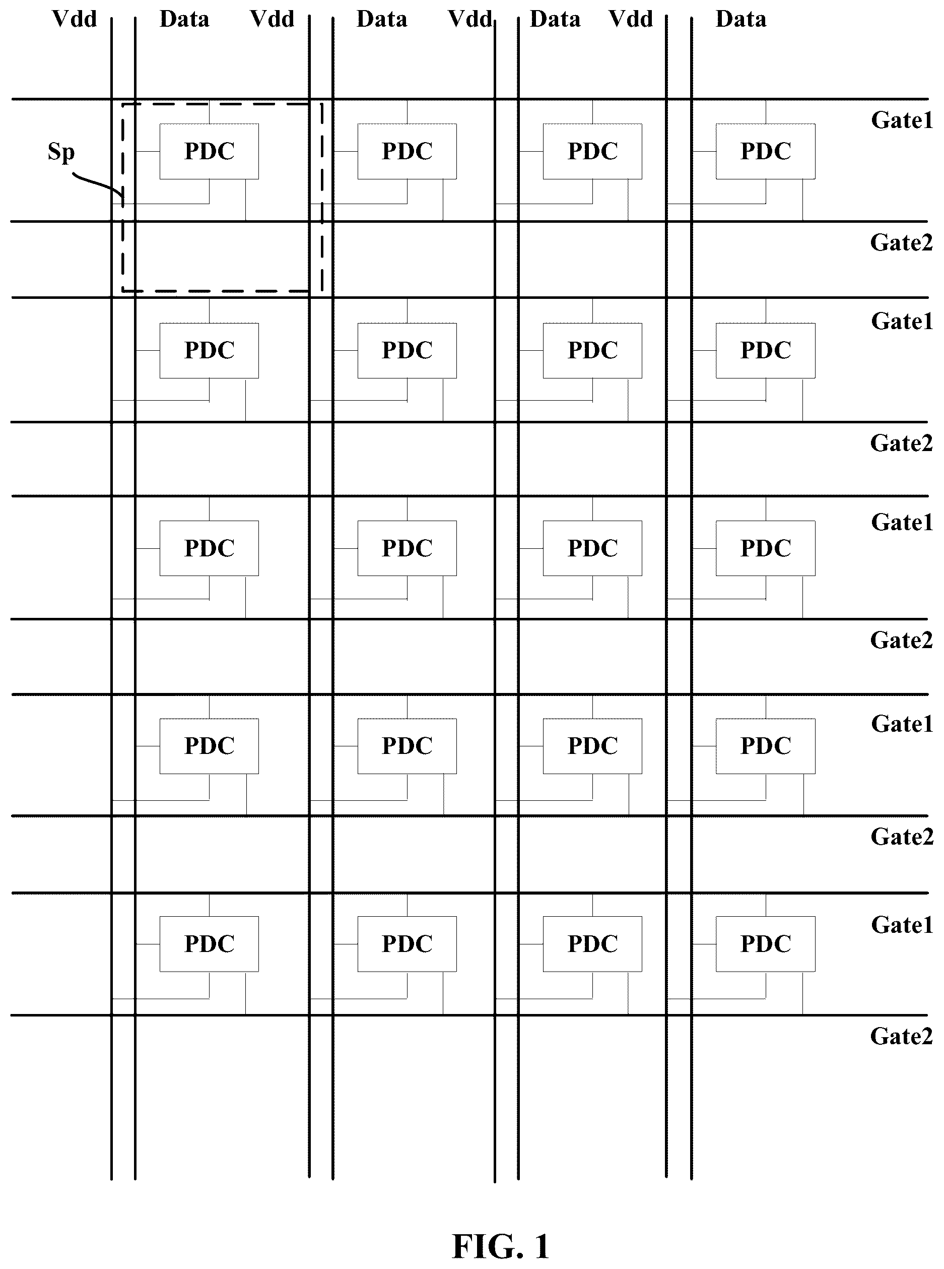
is a plan view of an array substrate in some embodiments according to the present disclosure. Referring to , the array substrate includes an array of subpixels Sp. Each subpixel includes an electronic component, e.g., a light emitting element. In one example, the light emitting element is driven by a respective pixel driving circuit PDC. The array substrate includes a plurality of first gate lines Gate 1 , a plurality of second gate lines Gate 2 , a plurality of data lines Data, a plurality of voltage supply line Vdd, and a respective second voltage supply line (e.g., a low voltage supply line Vss). Light emission in a respective subpixel Sp is driven by a respective pixel driving circuit PDC. In one example, a high voltage signal (e.g., a VDD signal) is input, through the respective high voltage supply line of the plurality of voltage supply line Vdd, to the respective pixel driving circuit PDC connected to an anode of the light emitting element; a low voltage signal (e.g., a VSS signal) is input, through a low voltage supply line Vss, to a cathode of the light emitting element. A voltage difference between the high voltage signal (e.g., the VDD signal) and the low voltage signal (e.g., the VSS signal) is a driving voltage ΔV that drives light emission in the light emitting element.
is a circuit diagram illustrating the structure of a pixel driving circuit in some embodiments according to the present disclosure. Referring to , the pixel driving circuit includes a driving transistor T 3 , a storage capacitor C 1 having a first capacitor electrode Ce 1 and a second capacitor electrode Ce 2 ; a coupling capacitor C 2 having a third capacitor electrode Ce 3 and a fourth capacitor electrode Ce 4 ; a data write transistor T 4 having a gate electrode connected to a first gate line Gate_N, a first electrode connected to a data line Data, and a second electrode connected to the first capacitor electrode Ce 1 and the fourth capacitor electrode Ce 4 . A gate electrode of the driving transistor T 3 is connected to the third capacitor electrode Ce 3 .
In some embodiments, the pixel driving circuit further includes a compensating transistor T 2 having a gate electrode connected to a first control signal line S 1 _N; a first electrode connected to the first capacitor electrode Ce 1 , the fourth capacitor electrode Ce 4 , and the second electrode of the data write transistor T 4 ; and a second electrode connected to a first electrode of the driving transistor T 3 .
In some embodiments, the first capacitor electrode Ce 1 of the storage capacitor C 1 is connected to the second electrode of the data write transistor T 4 , the first electrode of the compensating transistor T 2 , and the fourth capacitor electrode Ce 4 . The second capacitor electrode Ce 2 of the storage capacitor C 1 is connected to a first voltage supply line Vdd (e.g., a high voltage signal line).
In some embodiments, the fourth capacitor electrode Ce 4 of the coupling capacitor C 2 is connected to the second electrode of the data write transistor T 4 , the first electrode of the compensating transistor T 2 , and the first capacitor electrode Ce 1 . The third capacitor electrode Ce 3 of the coupling capacitor C 2 is connected to the gate electrode of the driving transistor T 3 .
In some embodiments, the pixel driving circuit further includes a light emitting control transistor T 5 having a gate electrode connected to a light emitting control signal line EM_N, a first electrode connected to the first voltage supply line Vdd, and a second electrode connected to the first electrode of the driving transistor T 3 and the second electrode of the compensating transistor T 2 .
In some embodiments, the pixel driving circuit further includes at least one reset transistor. In some embodiments, the pixel driving circuit further includes a first reset transistor T 1 having a gate electrode connected to a first control signal line S 1 _N, a first electrode connected to a first reset signal line Vint 1 , and a second electrode connected to the gate electrode of the driving transistor T 3 and the third capacitor electrode Ce 3 of the coupling capacitor C 2 .
In some embodiments, the pixel driving circuit further includes a second reset transistor T 7 having a gate electrode connected to a second control signal line S 2 _N, a first electrode connected to a second reset signal line Vint 2 , and a second electrode connected to the second electrode of the driving transistor T 3 and an anode of a light emitting element LE.
In some embodiments, the pixel driving circuit further includes a third reset transistor T 6 having a gate electrode connected to a third control signal line S 3 _N; a first electrode connected to a third reset signal line Vint 3 ; and a second electrode connected to the first electrode of the driving transistor T 3 , the second electrode of the light emitting control transistor T 5 , and the second electrode of the compensating transistor T 2 .
The pixel driving circuit further include a first node N 1 , a second node N 2 , a third node N 3 , and a fourth node N 4 . The first node N 1 is connected to the gate electrode of the driving transistor T 3 , the third capacitor electrode Ce 3 , and the second electrode of the first reset transistor T 1 . The second node N 2 is connected to the first electrode of the driving transistor T 3 , the second electrode of the light emitting control transistor T 5 , the second electrode of the compensating transistor T 2 , and the second electrode of the third reset transistor T 6 . The third node N 3 is connected to the second electrode of the data write transistor T 4 , the first electrode of the compensating transistor T 2 , the first capacitor electrode Ce 1 , and the fourth capacitor electrode Ce 4 . The fourth node N 4 is connected to the second electrode of the driving transistor T 3 , the second electrode of the second reset transistor T 7 , and the anode of the light emitting element LE.
As used herein, a first electrode or a second electrode refers to one of a first terminal and a second terminal of a transistor, the first terminal and the second terminal being connected to an active layer of the transistor. A direction of a current flowing through the transistor may be configured to be from a first electrode to a second electrode, or from a second electrode to a first electrode. Accordingly, depending on the direction of the current flowing through the transistor, in one example, the first electrode is configured to receive an input signal and the second electrode is configured to output an output signal; in another example, the second electrode is configured to receive an input signal and the first electrode is configured to output an output signal.
The present disclosure may be implemented in pixel driving circuit having transistors of various types, including a pixel driving circuit having p-type transistors, a pixel driving circuit having n-type transistors, and a pixel driving circuit having one or more p-type transistors and one or more n-type transistors. Referring to , the data write transistor T 4 , the compensating transistor T 2 , the first reset transistor T 1 , the second reset transistor T 7 , and the third reset transistor T 6 are n-type transistors such as metal oxide transistors, and the driving transistor T 3 and the light emitting control transistor T 5 are p-type transistors such as polysilicon transistors. For a p-type transistor, an effective control signal (e.g., a turn-on control signal) is a low voltage signal, and an ineffective control signal (e.g., a turn-off control signal) is a high voltage signal. For an n-type transistor, an effective control signal (e.g., a turn-on control signal) is a high voltage signal, and an ineffective control signal (e.g., a turn-off control signal) is a low voltage signal.
is a timing diagram illustrating the operation of a pixel driving circuit in some embodiments according to the present disclosure. Referring to and , during one frame of image, the operation of the pixel driving circuit includes a first phase t 1 , a second phase t 2 , a third phase t 3 , a fourth phase t 4 , and a fifth phase t 5 .
In the first phase t 1 , a turning-on control signal is provided through the first control signal line S 1 _N to the gate electrode of the first reset transistor T 1 to turn on the first reset transistor T 1 , allowing a reset signal from the first reset signal line Vint 1 to pass from a first electrode of the first reset transistor T 1 to a second electrode of the first reset transistor T 1 , and in turn to the third capacitor electrode Ce 3 and the gate electrode of the driving transistor T 3 . The node N 1 (the gate electrode of the driving transistor T 3 ) is reset. The turning-on control signal is also provided through the first control signal line S 1 _N to the gate electrode of the compensating transistor T 2 to turn on the compensating transistor T 2 . A turning-on control signal is provided through the second control signal line S 2 _N to the gate electrode of the second reset transistor T 7 to turn on the second reset transistor T 7 , allowing a reset signal from the second reset signal line Vint 2 to pass from a first electrode of the second reset transistor T 7 to a second electrode of the second reset transistor T 7 , and in turn to the second electrode of the driving transistor T 3 and the anode of the light emitting element LE. The node N 4 (the anode of the light emitting element LE) is reset. A turning-off light emitting control signal is provided through the light emitting control signal line EM_N to the gate electrode of the light emitting control transistor T 5 to turn off the light emitting control transistor T 5 . A turning-off control signal is provided through the third control signal line S 3 _N to the gate electrode of the third reset transistor T 6 to turn off the third reset transistor T 6 . A turning-off gate signal is provided through the first gate line Gate_N to the gate electrode of the data write transistor T 4 to turn off the data write transistor T 4 . A illustrates a current pathway in a phase t 1 of a frame of image in a pixel driving circuit in some embodiments according to the present disclosure. The shaded arrows in A indicates a current flow in the phase t 1 .
In the second phase t 2 , a turning-on control signal is provided through the first control signal line S 1 _N to the gate electrode of the first reset transistor T 1 to turn on the first reset transistor T 1 , and also provided through the first control signal line S 1 _N to the gate electrode of the compensating transistor T 2 to turn on the compensating transistor T 2 . A turning-on control signal is provided through the second control signal line S 2 _N to the gate electrode of the second reset transistor T 7 to turn on the second reset transistor T 7 . A turning-on control signal is provided through the third control signal line S 3 _N to the gate electrode of the third reset transistor T 6 to turn on the third reset transistor T 6 , allowing a reset signal from the third reset signal line Vint 3 to pass from a first electrode of the third reset transistor T 6 to a second electrode of the third reset transistor T 6 , and in turn to the first electrode of the driving transistor T 3 , the second electrode of the light emitting control transistor T 5 , and the second electrode of the compensating transistor T 2 . The node N 2 (the first electrode of the driving transistor T 3 ) is charged with a voltage of the third reset signal line Vint 3 . In some embodiments, the voltage of the third reset signal line Vint 3 has a high voltage level, to ensure Vgs<Vth, thereby ensuring the driving transistor T 3 remains in a turning-on state. B illustrates a current pathway in a phase t 2 of a frame of image in a pixel driving circuit in some embodiments according to the present disclosure. The shaded arrows in B indicates a current flow in the phase t 2 .
In the third phase t 3 (Vth compensating phase), a turning-off control signal is provided through the third control signal line S 3 _N to the gate electrode of the third reset transistor T 6 to turn off the third reset transistor T 6 . In the third phase t 3 , the first reset transistor T 1 , the compensating transistor T 2 , the driving transistor T 3 , and the second reset transistor T 7 remain turning on. A second reset signal is provided through the second reset signal line Vint 2 , the second reset signal passes through the second reset transistor T 7 and the driving transistor T 3 , charging the node N 2 (the first electrode of the driving transistor T 3 ). When the node N 2 is charged to a point when Vgs=Vth, the driving transistor T 3 is turned off. Vgs=VN 1 −VN 2 , wherein VN 1 is a voltage level at the node N 1 , and VN 2 is a voltage level at the node N 2 . In the third phase t 3 , VN 1 =a voltage level of the first reset signal provided by the first reset signal line Vint 1 . Thus, VN 2 =VN 1 −Vgs=VN 1 −Vth, i.e., VN 2 =Vint 1 −Vth. Because the compensating transistor T 2 is turning on in the third phase t 3 , VN 3 =VN 2 =VN 1 −Vth, wherein VN 3 is a voltage level at the node N 3 . C illustrates a current pathway in a phase t 3 of a frame of image in a pixel driving circuit in some embodiments according to the present disclosure. The shaded arrows in C indicates a current flow in the phase t 3 .
In the phase t 4 (data write phase), a turning-off control signal is provided through the first control signal line S 1 _N to the gate electrode of the first reset transistor T 1 to turn off the first reset transistor T 1 , and also provided through the first control signal line S 1 _N to the gate electrode of the compensating transistor T 2 to turn off the compensating transistor T 2 . A turning-off control signal is provided through the second control signal line S 2 _N to the gate electrode of the second reset transistor T 7 to turn off the second reset transistor T 7 . A turning-on gate signal is provided through the first gate line Gate_N to the gate electrode of the data write transistor T 4 to turn on the data write transistor T 4 , allowing a data signal provided through the data line Data to pass from a first electrode of the data write transistor T 4 to a second electrode of the data write transistor T 4 , and in turn to the node N 3 . In the phase t 3 , VN 1 =a voltage level of the first reset signal provided by the first reset signal line Vint 1 (denoted as Vre 1 ). In the phase t 4 , a voltage level at the node N 3 changes from (Vre 1 −Vth) to a voltage level of the data signal Vdata. The change is ΔVN 3 =Vdata−Vre 1 +Vth. The coupling capacitor C 2 induces a voltage coupling at the node N 1 by ΔVN 3 . Due to the voltage coupling, VN 1 changes to (Vre 1 +ΔVN 3 )=(Vre 1 +Vdata−Vre 1 +Vth)=(Vdata+Vth), wherein the Vdata is the voltage level of the data voltage signal, and the Vth is the voltage level of the threshold voltage Th of the PN junction of the driving transistor T 3 . D illustrates a current pathway in a phase t 4 of a frame of image in a pixel driving circuit in some embodiments according to the present disclosure. The shaded arrows in D indicates a current flow in the phase t 4 .
In the phase t 5 (light emission phase), a turning-on light emitting control signal is provided through the light emitting control signal line EM_N to the gate electrode of the light emitting control transistor T 5 to turn on the light emitting control transistor T 5 , allowing a first power supply voltage signal provided through the first voltage supply line Vdd to pass from a first electrode of the light emitting control transistor T 5 to a second electrode of the light emitting control transistor T 5 , in turn pass from a first electrode of the driving transistor T 3 to a second electrode of the driving transistor T 3 , and to the anode of the light emitting element LE. The light emitting element is configured to emit light. E illustrates a current pathway in a phase t 5 of a frame of image in a pixel driving circuit in some embodiments according to the present disclosure. The shaded arrows in E indicates a current flow in the phase t 5 .
The inventors of the present disclosure discover that, by having an n-type transistor (e.g., the data write transistor T 4 in ) between the data signal line Data and the node N 3 (the first electrode of the compensating transistor T 2 ), leakage current from the data signal line Data to the node N 3 can be effectively prevented. A voltage level at the node N 3 (the fourth capacitor electrode Ce 4 ) can be stabilized, and in turn a voltage level at the node N 1 (the third capacitor electrode Ce 3 ) can be stabilized. The n-type transistor (e.g., the data write transistor T 4 in ) is configured to control supply of the data signal to the node N 3 (the first electrode of the compensating transistor T 2 , the fourth capacitor electrode Ce 4 , the first capacitor electrode Ce 1 ).
The gate electrode of the n-type transistor configured to control supply of the data signal to the node N 3 is connected to a first gate line Gate_N. The inventors of the present disclosure discover that, when an effective control signal of a first gate scanning signal provided to the n-type transistor is pulse having a pulse width equal to or less than 1H, and the pulse has a high voltage level, the leakage current from the data signal line Data to the node N 3 can be effectively prevented. H refers to a period of a horizontal sync signal. A scan circuit (e.g., a gate driving circuit or a gate-on-array) can be used to provide the first gate scanning signal.
Various appropriate implementations may be practiced in the present disclosure. In the pixel driving circuit depicted in , the n-type transistor configured to control supply of the data signal to the node N 3 is the data write transistor T 4 having a first electrode connected to the data signal line. is a circuit diagram illustrating the structure of a pixel driving circuit in some embodiments according to the present disclosure. Referring to , the pixel driving circuit in some embodiments includes a driving transistor T 3 , a storage capacitor C 1 having a first capacitor electrode Ce 1 and a second capacitor electrode Ce 2 ; a coupling capacitor C 2 having a third capacitor electrode Ce 3 and a fourth capacitor electrode Ce 4 ; a data write transistor T 4 and a control transistor T 8 connect to each other. A gate electrode of the data write transistor T 4 is connected to a second gate line Gate_P, a first electrode of the data write transistor T 4 is connected to a data line Data, and a second electrode of the data write transistor T 4 is connected to a first electrode of the control transistor T 8 . A gate electrode of the control transistor T 8 is connected to a fourth control signal line S 4 _N, a first electrode of the control transistor T 8 is connected to the second electrode of the data write transistor T 4 , and a second electrode of the control transistor T 8 is connected to the first capacitor electrode Ce 1 and the fourth capacitor electrode Ce 4 . A gate electrode of the driving transistor T 3 is connected to the third capacitor electrode Ce 3 .
In some embodiments, the pixel driving circuit further includes a compensating transistor T 2 having a gate electrode connected to a first control signal line S 1 _N; a first electrode connected to the first capacitor electrode Ce 1 , the fourth capacitor electrode Ce 4 , and the second electrode of the control transistor T 8 ; and a second electrode connected to a first electrode of the driving transistor T 3 .
In some embodiments, the first capacitor electrode Ce 1 of the storage capacitor C 1 is connected to the second electrode of the control transistor T 8 , the first electrode of the compensating transistor T 2 , and the fourth capacitor electrode Ce 4 . The second capacitor electrode Ce 2 of the storage capacitor C 1 is connected to a first voltage supply line Vdd (e.g., a high voltage signal line).
In some embodiments, the fourth capacitor electrode Ce 4 of the coupling capacitor C 2 is connected to the second electrode of the control transistor T 8 , the first electrode of the compensating transistor T 2 , and the first capacitor electrode Ce 1 . The third capacitor electrode Ce 3 of the coupling capacitor C 2 is connected to the gate electrode of the driving transistor T 3 .
In some embodiments, the pixel driving circuit further includes a light emitting control transistor T 5 having a gate electrode connected to a light emitting control signal line EM_N, a first electrode connected to the first voltage supply line Vdd, and a second electrode connected to the first electrode of the driving transistor T 3 and the second electrode of the compensating transistor T 2 .
In some embodiments, the pixel driving circuit further includes at least one reset transistor. In some embodiments, the pixel driving circuit further includes a first reset transistor T 1 having a gate electrode connected to a first control signal line S 1 _N, a first electrode connected to a first reset signal line Vint 1 , and a second electrode connected to the gate electrode of the driving transistor T 3 and the third capacitor electrode Ce 3 of the coupling capacitor C 2 .
In some embodiments, the pixel driving circuit further includes a second reset transistor T 7 having a gate electrode connected to a second control signal line S 2 _N, a first electrode connected to a second reset signal line Vint 2 , and a second electrode connected to the second electrode of the driving transistor T 3 and an anode of a light emitting element LE.
In some embodiments, the pixel driving circuit further includes a third reset transistor T 6 having a gate electrode connected to a third control signal line S 3 _N; a first electrode connected to a third reset signal line Vint 3 ; and a second electrode connected to the first electrode of the driving transistor T 3 , the second electrode of the light emitting control transistor T 5 , and the second electrode of the compensating transistor T 2 .
The pixel driving circuit further include a first node N 1 , a second node N 2 , a third node N 3 , and a fourth node N 4 . The first node N 1 is connected to the gate electrode of the driving transistor T 3 , the third capacitor electrode Ce 3 , and the second electrode of the first reset transistor T 1 . The second node N 2 is connected to the first electrode of the driving transistor T 3 , the second electrode of the light emitting control transistor T 5 , the second electrode of the compensating transistor T 2 , and the second electrode of the third reset transistor T 6 . The third node N 3 is connected to the second electrode of the control transistor T 8 , the first electrode of the compensating transistor T 2 , the first capacitor electrode Ce 1 , and the fourth capacitor electrode Ce 4 . The fourth node N 4 is connected to the second electrode of the driving transistor T 3 , the second electrode of the second reset transistor T 7 , and the anode of the light emitting element LE.
The present disclosure may be implemented in pixel driving circuit having transistors of various types, including a pixel driving circuit having p-type transistors, a pixel driving circuit having n-type transistors, and a pixel driving circuit having one or more p-type transistors and one or more n-type transistors. Referring to , the control transistor T 8 , the compensating transistor T 2 , the first reset transistor T 1 , the second reset transistor T 7 , and the third reset transistor T 6 are n-type transistors such as metal oxide transistors; and the driving transistor T 3 , the data write transistor T 4 , and the light emitting control transistor T 5 are p-type transistors such as polysilicon transistors. For a p-type transistor, an effective control signal (e.g., a turn-on control signal) is a low voltage signal, and an ineffective control signal (e.g., a turn-off control signal) is a high voltage signal. For an n-type transistor, an effective control signal (e.g., a turn-on control signal) is a high voltage signal, and an ineffective control signal (e.g., a turn-off control signal) is a low voltage signal.
Various appropriate driving methods may be implemented in the present disclosure. is a timing diagram illustrating the operation of a pixel driving circuit in some embodiments according to the present disclosure. Referring to and , during one frame of image, the operation of the pixel driving circuit includes a first phase t 1 , a second phase t 2 , a third phase t 3 , a fourth phase t 4 , a fifth phase t 5 , a sixth phase t 6 , a seventh phase t 7 , and an eight phase t 8 .
In the first phase t 1 , a turning-on control signal is provided through the first control signal line S 1 _N to the gate electrode of the first reset transistor T 1 to turn on the first reset transistor T 1 , allowing a reset signal from the first reset signal line Vint 1 to pass from a first electrode of the first reset transistor T 1 to a second electrode of the first reset transistor T 1 , and in turn to the third capacitor electrode Ce 3 and the gate electrode of the driving transistor T 3 . The node N 1 (the gate electrode of the driving transistor T 3 ) is reset. The turning-on control signal is also provided through the first control signal line S 1 _N to the gate electrode of the compensating transistor T 2 to turn on the compensating transistor T 2 . A turning-on control signal is provided through the second control signal line S 2 _N to the gate electrode of the second reset transistor T 7 to turn on the second reset transistor T 7 , allowing a reset signal from the second reset signal line Vint 2 to pass from a first electrode of the second reset transistor T 7 to a second electrode of the second reset transistor T 7 , and in turn to the second electrode of the driving transistor T 3 and the anode of the light emitting element LE. The node N 4 (the anode of the light emitting element LE) is reset. A turning-off light emitting control signal is provided through the light emitting control signal line EM_N to the gate electrode of the light emitting control transistor T 5 to turn off the light emitting control transistor T 5 . A turning-off control signal is provided through the third control signal line S 3 _N to the gate electrode of the third reset transistor T 6 to turn off the third reset transistor T 6 . A turning-off gate signal is provided through the second gate line Gate_P to the gate electrode of the data write transistor T 4 to turn off the data write transistor T 4 . A turning-off control signal is provided through the fourth control signal line S 4 _N to the gate electrode of the control transistor T 8 to turn off the control transistor T 8 .
In the second phase t 2 , a turning-on control signal is provided through the first control signal line S 1 _N to the gate electrode of the first reset transistor T 1 to turn on the first reset transistor T 1 , and also provided through the first control signal line S 1 _N to the gate electrode of the compensating transistor T 2 to turn on the compensating transistor T 2 . A turning-on control signal is provided through the second control signal line S 2 _N to the gate electrode of the second reset transistor T 7 to turn on the second reset transistor T 7 . A turning-on control signal is provided through the third control signal line S 3 _N to the gate electrode of the third reset transistor T 6 to turn on the third reset transistor T 6 , allowing a reset signal from the third reset signal line Vint 3 to pass from a first electrode of the third reset transistor T 6 to a second electrode of the third reset transistor T 6 , and in turn to the first electrode of the driving transistor T 3 , the second electrode of the light emitting control transistor T 5 , and the second electrode of the compensating transistor T 2 . The node N 2 (the first electrode of the driving transistor T 3 ) is charged with a voltage of the third reset signal line Vint 3 . In some embodiments, the voltage of the third reset signal line Vint 3 has a high voltage level, to ensure Vgs<Vth, thereby ensuring the driving transistor T 3 remains in a turning-on state. A turning-off gate signal is provided through the second gate line Gate_P to the gate electrode of the data write transistor T 4 to turn off the data write transistor T 4 . A turning-off control signal is provided through the fourth control signal line S 4 _N to the gate electrode of the control transistor T 8 to turn off the control transistor T 8 .
In the third phase t 3 (Vth compensating phase), a turning-off control signal is provided through the third control signal line S 3 _N to the gate electrode of the third reset transistor T 6 to turn off the third reset transistor T 6 . In the third phase t 3 , the first reset transistor T 1 , the compensating transistor T 2 , the driving transistor T 3 , and the second reset transistor T 7 remain turning on. A second reset signal is provided through the second reset signal line Vint 2 , the second reset signal passes through the second reset transistor T 7 and the driving transistor T 3 , charging the node N 2 (the first electrode of the driving transistor T 3 ). When the node N 2 is charged to a point when Vgs=Vth, the driving transistor T 3 is turned off. Vgs=VN 1 −VN 2 , wherein VN 1 is a voltage level at the node N 1 , and VN 2 is a voltage level at the node N 2 . In the third phase t 3 , VN 1 =a voltage level of the first reset signal provided by the first reset signal line Vint 1 . Thus, VN 2 =VN 1 −Vgs=VN 1 −Vth, i.e., VN 2 =Vint 1 −Vth. Because the compensating transistor T 2 is turning on in the third phase t 3 , VN 3 =VN 2 =VN 1 −Vth, wherein VN 3 is a voltage level at the node N 3 . A turning-off gate signal is provided through the second gate line Gate_P to the gate electrode of the data write transistor T 4 to turn off the data write transistor T 4 . A turning-off control signal is provided through the fourth control signal line S 4 _N to the gate electrode of the control transistor T 8 to turn off the control transistor T 8 .
In the phase t 4 , a turning-off control signal is provided through the first control signal line S 1 _N to the gate electrode of the first reset transistor T 1 to turn off the first reset transistor T 1 , and also provided through the first control signal line S 1 _N to the gate electrode of the compensating transistor T 2 to turn off the compensating transistor T 2 . A turning-off control signal is provided through the second control signal line S 2 _N to the gate electrode of the second reset transistor T 7 to turn off the second reset transistor T 7 . Optionally, in the middle of the phase t 4 , a turning-on control signal is provided through the fourth control signal line S 4 _N to the gate electrode of the control transistor T 8 to turn on the control transistor T 8 . A turning-off gate signal is provided through the second gate line Gate_P to the gate electrode of the data write transistor T 4 to turn off the data write transistor T 4 . In the phase t 4 , the data signal is not provided to the node N 3 .
In the phase t 5 (data write phase), a turning-off control signal is provided through the first control signal line S 1 _N to the gate electrode of the first reset transistor T 1 to turn off the first reset transistor T 1 , and also provided through the first control signal line S 1 _N to the gate electrode of the compensating transistor T 2 to turn off the compensating transistor T 2 . A turning-off control signal is provided through the second control signal line S 2 _N to the gate electrode of the second reset transistor T 7 to turn off the second reset transistor T 7 . A turning-on control signal is provided through the fourth control signal line S 4 _N to the gate electrode of the control transistor T 8 to turn on the control transistor T 8 . In the phase t 5 , a turning-on gate signal is provided through the second gate line Gate_P to the gate electrode of the data write transistor T 4 to turn on the data write transistor T 4 . In the phase t 5 , both the data write transistor T 4 and the control transistor T 8 are turned on, allowing a data signal provided through the data line Data to pass from a first electrode of the data write transistor T 4 to a second electrode of the data write transistor T 4 , then pass from a first electrode of the control transistor T 8 to a second electrode of the control transistor T 8 , and in turn to the node N 3 . In the phase t 4 , VN 1 =a voltage level of the first reset signal provided by the first reset signal line Vint 1 (denoted as Vre 1 ). In the phase t 5 , a voltage level at the node N 3 changes from (Vre 1 −Vth) to a voltage level of the data signal Vdata. The change is ΔVN 3 =Vdata−Vre 1 +Vth. The coupling capacitor C 2 induces a voltage coupling at the node N 1 by ΔVN 3 . Due to the voltage coupling, VN 1 changes to (Vre 1 +ΔVN 3 )=(Vre 1 +Vdata−Vre 1 +Vth)=(Vdata+Vth), wherein the Vdata is the voltage level of the data voltage signal, and the Vth is the voltage level of the threshold voltage Th of the PN junction of the driving transistor T 3 .
In the phase t 6 , a turning-off gate signal is provided through the second gate line Gate_P to the gate electrode of the data write transistor T 4 to turn off the data write transistor T 4 . In the middle of the phase t 6 , a turning-off control signal is provided through the fourth control signal line S 4 _N to the gate electrode of the control transistor T 8 to turn off the control transistor T 8 . Both the data write transistor T 4 and the control transistor T 8 are turned off, effectively preventing leakage current from the data signal line Data.
In the phase t 7 (light emission phase), a turning-on light emitting control signal is provided through the light emitting control signal line EM_N to the gate electrode of the light emitting control transistor T 5 to turn on the light emitting control transistor T 5 , allowing a first power supply voltage signal provided through the first voltage supply line Vdd to pass from a first electrode of the light emitting control transistor T 5 to a second electrode of the light emitting control transistor T 5 , in turn pass from a first electrode of the driving transistor T 3 to a second electrode of the driving transistor T 3 , and to the anode of the light emitting element LE. The light emitting element is configured to emit light.
The phase t 8 is a blanking phase of the frame of image.
Referring to , in some embodiments, a first period during which the control transistor T 8 is turned on is longer than a second period during which the data write transistor T 4 is turned on. The second period is a sub-period of the first period.
The inventors of the present disclosure discover that, by having an n-type transistor (e.g., the control transistor T 8 in ) between the data signal line Data and the node N 3 (the first electrode of the compensating transistor T 2 ), leakage current from the data signal line Data to the node N 3 can be effectively prevented. A voltage level at the node N 3 (the fourth capacitor electrode Ce 4 ) can be stabilized, and in turn a voltage level at the node N 1 (the third capacitor electrode Ce 3 ) can be stabilized. The n-type transistor (e.g., the control transistor T 8 in in concert with the data write transistor T 4 ) is configured to control supply of the data signal to the node N 3 (the first electrode of the compensating transistor T 2 , the fourth capacitor electrode Ce 4 , the first capacitor electrode Ce 1 ).
The gate electrode of the data write transistor T 4 is controlled by the second gate scanning signal provided by the second gate line Gate_P, the gate electrode of the control transistor T 8 is controlled by a fourth control signal provided by the fourth control signal line S 4 _N. Two different scan circuits may be used to provide the second gate scanning signal to the second gate line Gate_P, and provide the fourth control signal to the fourth control signal line S 4 _N. For example, a gate scanning signal generating circuit is configured to generate gate scanning signals for the second gate line Gate_P, and a light emitting control signal generating circuit is configured to generate control signals for the fourth control signal line S 4 _N.
Various alternative driving methods may be practiced in the present disclosure. For example, the fourth control signal line S 4 _N may share a same scan circuit with one or more control signal lines or gate lines, however, configured to receive an output from the same scan circuit at a different stage. Optionally, the one or more control signal lines or gate lines are configured to receive an output signal of a present stage, and the fourth control signal line S 4 _N is configured to receive an output signal of a previous stage. Optionally, the one or more control signal lines or gate lines are configured to receive an output signal of a present stage, and the fourth control signal line S 4 _N is configured to receive an output signal of a later stage. Optionally, the one or more control signal lines or gate lines are configured to receive a m-th stage output from the same scan circuit, and the fourth control signal line S 4 _N is configured to receive a (m−n)-th stage output from the same scan circuit, m and n being positive integers, m>n. Optionally, the one or more control signal lines or gate lines are configured to receive a m-th stage output from the same scan circuit, and the fourth control signal line S 4 _N is configured to receive a (m+n)-th stage output from the same scan circuit, m and n being positive integers, n>m.
is a timing diagram illustrating the operation of a pixel driving circuit in some embodiments according to the present disclosure. Referring to , the fourth control signal line S 4 _N and the first control signal line S 1 _N are configured to receive output signals of different stages, respectively, from a same scan circuit. Optionally, the first control signal line S 1 _N is configured to receive an output signal of a present stage, and the fourth control signal line S 4 _N is configured to receive an output signal of a previous stage (not necessarily an immediately previous stage). An effective voltage of the output signal from the same scan circuit is provided to the fourth control signal line S 4 _N at a time point in the middle of the phase t 4 , e.g., after the output signal provided to the first control signal line S 1 _N becomes an ineffective voltage. The second control signal line S 2 _N and the third control signal line S 3 _N are configured to receive control signals from independent scan circuits, so that the first electrode and the gate electrode of the driving transistor T 3 can be reset during the blanking period t 8 , reducing flicker and residual image.
The present disclosure may be implemented in pixel driving circuit having transistors of various types, including a pixel driving circuit having p-type transistors, a pixel driving circuit having n-type transistors, and a pixel driving circuit having one or more p-type transistors and one or more n-type transistors. is a circuit diagram illustrating the structure of a pixel driving circuit in some embodiments according to the present disclosure. Referring to , the control transistor T 8 , the compensating transistor T 2 , the first reset transistor T 1 , and the second reset transistor T 7 are n-type transistors such as metal oxide transistors; and the driving transistor T 3 , the data write transistor T 4 , the light emitting control transistor T 5 , and the third reset transistor T 6 are p-type transistors such as polysilicon transistors. For a p-type transistor, an effective control signal (e.g., a turn-on control signal) is a low voltage signal, and an ineffective control signal (e.g., a turn-off control signal) is a high voltage signal. For an n-type transistor, an effective control signal (e.g., a turn-on control signal) is a high voltage signal, and an ineffective control signal (e.g., a turn-off control signal) is a low voltage signal.
Various alternative driving methods may be practiced in the present disclosure. For example, the third control signal line S 3 _N may share a same scan circuit with one or more control signal lines or gate lines, however, configured to receive an output from the same scan circuit at a different stage. Optionally, the one or more control signal lines or gate lines are configured to receive an output signal of a present stage, and the third control signal line S 3 _N is configured to receive an output signal of a previous stage. Optionally, the one or more control signal lines or gate lines are configured to receive an output signal of a present stage, and the third control signal line S 3 _N is configured to receive an output signal of a later stage. Optionally, the one or more control signal lines or gate lines are configured to receive a m-th stage output from the same scan circuit, and the third control signal line S 3 _N is configured to receive a (m-n)-th stage output from the same scan circuit, m and n being positive integers, m>n. Optionally, the one or more control signal lines or gate lines are configured to receive a m-th stage output from the same scan circuit, and the third control signal line S 3 _N is configured to receive a (m+n)-th stage output from the same scan circuit, m and n being positive integers, n>m.
In another example, the fourth control signal line S 4 _N may share a same scan circuit with one or more control signal lines or gate lines, however, configured to receive an output from the same scan circuit at a different stage. Optionally, the one or more control signal lines or gate lines are configured to receive an output signal of a present stage, and the fourth control signal line S 4 _N is configured to receive an output signal of a previous stage. Optionally, the one or more control signal lines or gate lines are configured to receive an output signal of a present stage, and the fourth control signal line S 4 _N is configured to receive an output signal of a later stage. Optionally, the one or more control signal lines or gate lines are configured to receive a m-th stage output from the same scan circuit, and the fourth control signal line S 4 _N is configured to receive a (m−n)-th stage output from the same scan circuit, m and n being positive integers, m>n. Optionally, the one or more control signal lines or gate lines are configured to receive a m-th stage output from the same scan circuit, and the fourth control signal line S 4 _N is configured to receive a (m+n)-th stage output from the same scan circuit, m and n being positive integers, n>m.
is a timing diagram illustrating the operation of a pixel driving circuit in some embodiments according to the present disclosure. Referring to and , the third control signal line S 3 _N and the second gate line Gate_P are configured to receive output signals of different stages, respectively, from a same scan circuit (e.g., a same gate scanning signal generating circuit). Optionally, the second gate line Gate_P is configured to receive an output signal of a present stage, and the third control signal line S 3 _N is configured to receive an output signal of a previous stage (not necessarily an immediately previous stage).
Referring to and , the fourth control signal line S 4 _N and the first control signal line S 1 _N are configured to receive output signals of different stages, respectively, from a same scan circuit. Optionally, the first control signal line S 1 _N is configured to receive an output signal of a present stage, and the fourth control signal line S 4 _N is configured to receive an output signal of a previous stage (not necessarily an immediately previous stage). An effective voltage of the output signal from the same scan circuit is provided to the fourth control signal line S 4 _N at a time point in the middle of the phase t 4 , e.g., after the output signal provided to the first control signal line S 1 _N becomes an ineffective voltage. The second control signal line S 2 _N and the third control signal line S 3 _N are configured to receive control signals from independent scan circuits, so that the first electrode and the gate electrode of the driving transistor T 3 can be reset during the blanking period t 8 , reducing flicker and residual image.
In another aspect, the present disclosure provides a display panel having the pixel driving circuit described herein, and one or more scan circuits configured to provide control signals to the pixel driving circuit. Various appropriate scan circuits may be implemented in the present disclosure. In some embodiments, each of the one or more scan circuits includes a plurality of stages of cascaded scan units. Optionally, the plurality of stages of cascaded scan units are configured to provide a plurality of control signals to a plurality of rows of pixel driving circuits.
A is a schematic diagram illustrating the structure of a scan circuit in some embodiments according to the present disclosure. Referring to A , the scan circuit in some embodiments includes N number of stages. A respective stage of the N number of stages includes a respective scan unit. As depicted in A , the scan circuit includes a 1 st scan unit, a 2 nd scan unit, a 3 rd scan unit, a 4 th scan unit, . . . , an N-th scan unit. The N number of scan units are configured to provide N number of control signals (e.g., gate scanning signals, reset control signals, or light emission control signals) to N number of rows of subpixels. The N number of control signals are denoted as Output 1 , Output 2 , Output 3 , Output 4 , . . . , OutputN in A . An n-th scan unit is configured to receive a start signal SS or an output signal from an output terminal of a previous scan unit (e.g., a (n−1)-th scan unit, a (n−2)-th scan unit, or a (n−3)-th scan unit). As used herein, the term “previous scan unit” is not limited to immediately previous scan unit (e.g., the (n−1)-th scan unit), but includes any appropriate previous scan unit (e.g., the (n−2)-th scan unit, or the (n−3)-th scan unit). In A , the 1 st scan unit is configured to receive the start signal SS as the input signal, the 2 nd scan unit is configured to receive an output signal from the 1 st scan unit as an input signal Input 2 , the 3 rd scan unit is configured to receive an output signal from the 2 nd scan unit as an input signal Input 3 , the 4 th scan unit is configured to receive an output signal from the 3 rd scan unit as an input signal Input 4 , the N-th scan unit is configured to receive an output signal from the (N−1)-th scan unit as an input signal InputN.
Referring to A , an n-th scan unit is configured to receive an output signal from a subsequent scan unit (e.g., a (n+1)-th scan unit, a (n+2)-th scan unit, or a (n+3)-th scan unit) as a reset signal. As used herein, the term “subsequent scan unit” is not limited to immediately subsequent scan unit (e.g., the (n+1)-th scan unit), but includes any appropriate subsequent scan unit (e.g., the (n+2)-th scan unit, or the (n+3)-th scan unit). In A , the 1 st scan unit is configured to receive an output signal from the 2nd scan unit as a reset signal Reset 1 , the 2 nd scan unit is configured to receive an output signal from the 3 rd scan unit as a reset signal Reset 2 , the 3 rd scan unit is configured to receive an output signal from the 4 th scan unit as a reset signal Reset 3 , and the 4 th scan unit is configured to receive an output signal from the 5 th scan unit as a reset signal Reset 4 .
In some embodiments, the scan circuit may be operated in a forward scanning mode and a reverse scanning mode. A illustrates the forward scanning mode of the scan circuit. B is a schematic diagram illustrating the structure of a scan circuit in some embodiments according to the present disclosure. B illustrates the reverse scanning mode of the scan circuit. Referring to B , an n-th scan unit is configured to receive a start signal SS or an output signal from an output terminal of a subsequent scan unit (e.g., a (n+1)-th scan unit, a (n+2)-th scan unit, or a (n+3)-th scan unit). In B , the N-th scan unit is configured to receive the start signal SS as the input signal, the 4 th scan unit is configured to receive an output signal from a 5 th scan unit as an input signal Input 4 , the 3 rd scan unit is configured to receive an output signal from the 4 th scan unit as an input signal Input 3 , the 2 nd scan unit is configured to receive an output signal from the 3 rd scan unit as an input signal Input 2 ; and the 1 st scan unit is configured to receive an output signal from the 2 nd scan unit as an input signal Input 1 .
Referring to B , in the reverse scanning mode, an n-th scan unit is configured to receive an output signal from a previous scan unit (e.g., a (n−1)-th scan unit, a (n−2)-th scan unit, or a (n−3)-th scan unit) as a reset signal. In B , the 2 nd scan unit is configured to receive an output signal from the 1 st scan unit as a reset signal Reset 2 , the 3 rd scan unit is configured to receive an output signal from the 2 nd scan unit as a reset signal Reset 3 , the 4 th scan unit is configured to receive an output signal from the 3 rd scan unit as a reset signal Reset 4 , and the 5 th scan unit is configured to receive an output signal from the 4 th scan unit as a reset signal Reset 5 .
is a circuit diagram of a scan unit in a scan circuit in some embodiments according to the present disclosure. Referring to , the scan unit in some embodiments includes a first control transistor T 1 to an eighth control transistor T 8 , a first control capacitor C 1 and a second control capacitor C 2 . In some embodiments, a gate electrode of the first control transistor T 1 is electrically connected to a first clock signal terminal CK, a first electrode of the first control transistor T 1 is electrically connected to an input terminal IN, a second electrode of the first control transistor T 1 is electrically connected to a first node G 1 ; a gate electrode of the second control transistor T 2 is electrically connected to the first node G 1 , a first electrode of the second control transistor T 2 is electrically connected to the first clock signal terminal CK, the second electrode of the second control transistor T 2 is electrically connected to a second node G 2 ; a gate electrode of the third control transistor T 3 is electrically connected to a first clock signal terminal CK, a first electrode of the third control transistor T 3 is electrically connected to a second power supply VGL, a second electrode of the third control transistor T 3 is electrically connected to the second node G 2 ; a gate electrode of the fourth control transistor T 4 is electrically connected to the second node G 2 , a first electrode of the fourth control transistor T 4 is electrically connected to a first power supply VGH, a second electrode of the fourth control transistor T 4 is electrically connected to an output terminal OUT; a gate electrode of the fifth control transistor T 5 is electrically connected to a third node G 3 , a first electrode of the fifth control transistor T 5 is electrically connected to a second clock signal terminal CB, a second electrode of the fifth control transistor T 5 is electrically connected to the output terminal OUT; a gate electrode of the sixth control transistor T 6 is electrically connected to the second node G 2 , a first electrode of the sixth control transistor T 6 is electrically connected to the first power supply VGH, a second electrode of the sixth control transistor T 6 is electrically connected to a first electrode of a seventh control transistor T 7 ; a gate electrode of the seventh control transistor T 7 is electrically connected to the second clock signal terminal CB, a second electrode of the seventh control transistor T 7 is electrically connected to the first node G 1 ; a gate electrode of the eighth control transistor T 8 is electrically connected to a second power supply VGL, a first electrode of the eighth control transistor T 8 is electrically connected to the first node G 1 , a second electrode of the eighth control transistor T 8 is electrically connected to a third node G 3 ; a first electrode plate C 11 of a first control capacitor C 1 is electrically connected to the second node G 2 , a second electrode plate C 12 of the first control capacitor C 1 is electrically connected to the first power supply VGH; and a first electrode plate C 21 of a second control capacitor C 2 is electrically connected to the third node G 3 , and a second electrode plate C 22 of the second control capacitor C 2 is electrically connected to the output terminal OUT. In one example, the first control transistor T 1 to the eighth control transistor T 8 may be a p-type transistor or may be an n-type transistor. In another example, the first power supply VGH provides a continuous high level signal and the second power supply VGL provides a continuous low level signal.
In one example, the scan circuit depicted in may be configured to provide control signals to the second gate line Gate_P in the pixel driving circuits depicted in and .
is a circuit diagram of a scan unit in a scan circuit in some embodiments according to the present disclosure. Referring to , the scan unit in some embodiments includes an input subcircuit ISC, an output subcircuit OSC, a first processing subcircuit PSC 1 , a second processing subcircuit PSC 2 , a third processing subcircuit PSC 3 , and a stabilizing subcircuit SSC.
In some embodiments, the output subcircuit OSC is configured to supply the voltage of a first power supply VGH or a second power supply VGL to an output terminal TM 4 in response to voltages of a fourth node N 4 and a first node N 1 . Optionally, the output subcircuit OSC includes a ninth transistor T 9 and a tenth transistor T 10 .
The ninth transistor T 9 is coupled between a first power supply VGH and the output terminal TM 4 . A gate electrode of the ninth transistor T 9 is coupled to the fourth node N 4 . The ninth transistor T 9 may be turned on or off depending on the voltage of the fourth node N 4 . Optionally, when the ninth transistor T 9 is turned on, the voltage of the first power supply VGH is provided to the output terminal TM 4 , which (annotated as Outc in ) may be transmitted to an n-th gate line and used as a gate driving signal having a gate-on level.
The tenth transistor T 10 is coupled between the output terminal TM 4 and a second power supply VGL. A gate electrode of the tenth transistor T 10 is coupled to the first node N 1 . The tenth transistor T 10 may be turned on or off depending on the voltage of the first node N 1 . Optionally, when the tenth transistor T 10 is turned on, the voltage of the second power supply VGL is provided to the output terminal TM 4 , which (annotated as Outc in ) may be provided to an n-th gate line and used as a gate driving signal having a gate-off level. In one example, when the gate driving signal has a gate-off level, it may be understood that the gate driving signal is not provided.
In some embodiments, the input subcircuit ISC is configured to control the voltages of the first node N 1 in response to signals provided to the first input terminal TM 1 and the second input terminal TM 2 , respectively. Optionally, the input subcircuit ISC includes a first transistor T 1 .
The first transistor T 1 is coupled between the first input terminal TM 1 and the first node N 1 . A gate electrode of the first transistor T 1 is coupled to the second input terminal TM 2 . When the first clock signal CK is provided to the second input terminal TM 2 , the first transistor T 1 is turned on to electrically couple the first input terminal TM 1 with the first node N 1 .
In some embodiments, the first processing subcircuit PSC 1 is configured to control the voltage of the fourth node N 4 in response to the voltage of the first node N 1 . Optionally, the first processing subcircuit PSC 1 includes an eighth transistor T 8 and a second capacitor C 2 .
The eighth transistor T 8 is coupled between the first power supply VGH and the fourth node N 4 . A gate electrode of the eighth transistor T 8 is coupled to the first node N 1 . The eighth transistor T 8 may be turned on or off depending on the voltage of the first node N 1 . Optionally, when the eighth transistor T 8 is turned on, the voltage of the first power supply VGH may be provided to the fourth node N 4 .
The second capacitor C 2 is coupled between the first power supply VGH and the fourth node N 4 . Optionally, the second capacitor C 2 is configured to charge a voltage to be applied to the fourth node N 4 . Optionally, the second capacitor C 2 is configured to stably maintain the voltage of the fourth node N 4 .
In some embodiments, the second processing subcircuit PSC 2 is coupled to the second node N 2 , and is configured to control the voltage of the fourth node N 4 in response to a signal input to the third input terminal TM 3 . Optionally, the second processing subcircuit PSC 2 includes a sixth transistor T 6 , a seventh transistor T 7 , and a first capacitor C 1 .
A first terminal of the first capacitor C 1 is coupled to the second node N 2 , and a second terminal of the first capacitor C 1 is coupled to a third node N 3 that is a common node between the sixth transistor T 6 and the seventh transistor T 7 .
The sixth transistor T 6 is coupled between the third node N 3 and the second node N 2 . A gate electrode of the sixth transistor T 6 is coupled to the second node N 2 . The sixth transistor T 6 may be turned on depending on the voltage of the second node N 2 so that a voltage corresponding to the second clock signal CB provided to the third input terminal TM 3 may be applied to the third node N 3 .
The seventh transistor T 7 is coupled between the fourth node N 4 and the third node N 3 . A gate electrode of the seventh transistor T 7 is coupled to the third input terminal TM 3 . The seventh transistor T 7 may be turned on in response to the second clock signal CB provided to the third input terminal TM 3 , and thus, applies the voltage of the first power supply VGH to the third node N 3 .
In some embodiments, the third processing subcircuit PSC 3 is configured to control the voltage of the second node N 2 . Optionally, the third processing subcircuit PSC 3 includes a second transistor T 2 , a third transistor T 3 , a fourth transistor T 4 , and a fifth transistor T 5 .
The fifth transistor T 5 is coupled between the first power supply VGH and the fourth transistor T 4 . A gate electrode of the fifth transistor T 5 is coupled to the second node N 2 . The fifth transistor T 5 may be turned on or off depending on the voltage of the second node N 2 .
The fourth transistor T 4 is coupled between the fifth transistor T 5 and the first node N 1 . A gate electrode of the fourth transistor T 4 is configured to be provided with the second clock signal CB provided to the third input terminal TM 3 .
The second transistor T 2 is coupled between the second node N 2 and the second input terminal TM 2 . A gate electrode of the second transistor T 2 is coupled to the first node N 1 .
The third transistor T 3 is coupled between the second node N 2 and the second power supply VGL. A gate electrode of the third transistor T 3 is coupled to the second input terminal TM 2 . When the first clock signal CK is provided to the second input terminal TM 2 , the third transistor T 3 may be turned on so that the voltage of the second power supply VGL may be provided to the second node N 2 .
In some embodiments, the stabilizing subcircuit SSC is coupled between the input subcircuit ISC and the output subcircuit OSC. Optionally, the stabilizing subcircuit SSC is configured to limit a voltage drop width of the first node N 1 . Optionally, the stabilizing subcircuit SSC includes a third capacitor C 3 .
A first electrode of the third capacitor C 3 is coupled to the gate electrode of the tenth transistor T 10 , and a second electrode of the third capacitor C 3 is configured to be provided with the second clock signal CB provided to the third input terminal TM 3 .
In some embodiments, referring to , each of the first to tenth transistors T 1 to T 10 may be formed of a p-type transistor. In some embodiments, the gate-on voltage of the first to tenth transistors T 1 to T 10 may be set to a low level, and the gate-off voltage thereof may be set to a high level.
In alternative embodiments, each of the first to tenth transistors T 1 to T 10 may be formed of an n-type transistor. In some embodiments, the gate-on voltage of the first to tenth transistors T 1 to T 10 may be set to a high level, and the gate-off voltage thereof may be set to a low level.
In one example, the scan circuit depicted in may be configured to provide control signals to at least one of the first control signal line S 1 _N, the second control signal line S 2 _N, the third control signal line S 3 _N, the fourth control signal line S 4 _N, or the first gate line Gate_N depicted in , , or .
is a circuit diagram of a scan unit in a scan circuit in some embodiments according to the present disclosure. Referring to , the respective scan unit in some embodiments includes an input subcircuit ISC, an output subcircuit OSC, a first processing subcircuit PSC 1 , a second processing subcircuit PSC 2 , a third processing subcircuit PSC 3 , a first stabilizing subcircuit SSC 1 , and a second stabilizing subcircuit SSC 2 . A respective scan unit may be configured to transmit control signals to one or more rows of subpixels. In one example, the respective scan unit is configured to transmit control signals to a single row of subpixels. In another example, the respective scan unit is configured to transmit control signals to two or more rows of subpixels.
In some embodiments, the output subcircuit OSC is configured to supply the voltage of a first power supply VGH or a second power supply VGL to an output terminal TM 4 in response to voltages of a fourth node N 4 and a first node N 1 . Optionally, the output subcircuit OSC includes a ninth transistor T 9 and a tenth transistor T 10 .
The ninth transistor T 9 is coupled between a first power supply VGH and the output terminal TM 4 . A gate electrode of the ninth transistor T 9 is coupled to the fourth node N 4 . The ninth transistor T 9 may be turned on or off depending on the voltage of the fourth node N 4 . Optionally, when the ninth transistor T 9 is turned on, the voltage of the first power supply VGH is provided to the output terminal TM 4 , which (annotated as Outc in ) may be transmitted to an n-th gate line and used as a gate driving signal having a gate-on level.
The tenth transistor T 10 is coupled between the output terminal TM 4 and a second power supply VGL. A gate electrode of the tenth transistor T 10 is coupled to the first node N 1 . The tenth transistor T 10 may be turned on or off depending on the voltage of the first node N 1 . Optionally, when the tenth transistor T 10 is turned on, the voltage of the second power supply VGL is provided to the output terminal TM 4 , which (annotated as Outc in ) may be provided to an n-th gate line and used as a gate driving signal having a gate-off level. In one example, when the gate driving signal has a gate-off level, it may be understood that the gate driving signal is not provided.
In some embodiments, the input subcircuit ISC is configured to control the voltages of the first node N 1 in response to signals provided to the first input terminal TM 1 and the second input terminal TM 2 , respectively. Optionally, the input subcircuit ISC includes a first transistor T 1 .
The first transistor T 1 is coupled between the first input terminal TM 1 and the first node N 1 . A gate electrode of the first transistor T 1 is coupled to the second input terminal TM 2 . When the first clock signal CK is provided to the second input terminal TM 2 , the first transistor T 1 is turned on to electrically couple the first input terminal TM 1 with the first node N 1 .
In some embodiments, the first processing subcircuit PSC 1 is configured to control the voltage of the fourth node N 4 in response to the voltages of the first node N 1 . Optionally, the first processing subcircuit PSC 1 includes an eighth transistor T 8 and a second capacitor C 2 .
The eighth transistor T 8 is coupled between the first power supply VGH and the fourth node N 4 . A gate electrode of the eighth transistor T 8 is coupled to the first node N 1 . The eighth transistor T 8 may be turned on or off depending on the voltage of the first node N 1 . Optionally, when the eighth transistor T 8 is turned on, the voltage of the first power supply VGH may be provided to the fourth node N 4 .
The second capacitor C 2 is coupled between the first power supply VGH and the fourth node N 4 . Optionally, the second capacitor C 2 is configured to charge a voltage to be applied to the fourth node N 4 . Optionally, the second capacitor C 2 is configured to stably maintain the voltage of the fourth node N 4 .
In some embodiments, the second processing subcircuit PSC 2 is coupled to a fifth node N 5 , and is configured to control the voltage of the fourth node N 4 in response to a signal input to the third input terminal TM 3 . Optionally, the second processing subcircuit PSC 2 includes a sixth transistor T 6 , a seventh transistor T 7 , and a first capacitor C 1 .
A first terminal of the first capacitor C 1 is coupled to the fifth node N 5 , and a second terminal of the first capacitor C 1 is coupled to a third node N 3 that is a common node between the sixth transistor T 6 and the seventh transistor T 7 .
The sixth transistor T 6 is coupled between the third node N 3 and the fifth node N 5 . A gate electrode of the sixth transistor T 6 is coupled to the fifth node N 5 . The sixth transistor T 6 may be turned on depending on the voltage of the fifth node N 5 so that a voltage corresponding to the second clock signal CB provided to the third input terminal TM 3 may be applied to the third node N 3 .
The seventh transistor T 7 is coupled between the fourth node N 4 and the third node N 3 . A gate electrode of the seventh transistor T 7 is coupled to the third input terminal TM 3 . The seventh transistor T 7 may be turned on in response to the second clock signal CB provided to the third input terminal TM 3 , and thus, applies the voltage of the first power supply VGH to the third node N 3 .
In some embodiments, the third processing subcircuit PSC 3 is configured to control the voltage of the second node N 2 . Optionally, the third processing subcircuit PSC 3 includes a second transistor T 2 , a third transistor T 3 , a fourth transistor T 4 , a fifth transistor T 5 , and a third capacitor C 3 .
The fifth transistor T 5 is coupled between the first power supply VGH and the fourth transistor T 4 . A gate electrode of the fifth transistor T 5 is coupled to the second node N 2 . The fifth transistor T 5 may be turned on or off depending on the voltage of the second node N 2 .
The fourth transistor T 4 is coupled between the fifth transistor T 5 and the third input terminal TM 3 . A first electrode of the fourth transistor T 4 is configured to be provided with the second clock signal CB provided to the third input terminal TM 3 . A gate electrode of the fourth transistor T 4 is coupled to the gate electrode of the tenth transistor T 10 . A second electrode of the fourth transistor T 4 is coupled to the second electrode of the fifth transistor T 5 .
The second transistor T 2 is coupled between the second node N 2 and the second input terminal TM 2 . A gate electrode of the second transistor T 2 is coupled to the first node N 1 .
The third transistor T 3 is coupled between the second node N 2 and the second power supply VGL. A gate electrode of the third transistor T 3 is coupled to the second input terminal TM 2 . When the first clock signal CK is provided to the second input terminal TM 2 , the third transistor T 3 may be turned on so that the voltage of the second power supply VGL may be provided to the second node N 2 .
The third capacitor C 3 is coupled between the tenth transistor T 10 and the fifth transistor T 5 . A first capacitor electrode of the third capacitor C 3 is coupled to the second electrode of the fifth transistor T 5 and the first electrode of the fourth transistor T 4 . A second capacitor electrode of the third capacitor C 3 is coupled to the gate electrode of the fourth transistor T 4 and the gate electrode of the tenth transistor T 10 .
In some embodiments, the first stabilizing subcircuit SSC 1 is coupled between the second processing subcircuit PSC 2 and the third processing subcircuit PSC 3 . Optionally, the first stabilizing subcircuit SSC 1 is configured to limit a voltage drop width of the second node N 2 . Optionally, the first stabilizing subcircuit SSC 1 includes an eleventh transistor T 11 .
The eleventh transistor T 11 is coupled between the second node N 2 and the fifth node N 5 . A gate electrode of the eleventh transistor T 11 is coupled to the second power supply VGL. Since the second power supply VGL has a gate-on level voltage, the eleventh transistor T 11 may always remain turned on. Therefore, the second node N 2 and the fifth node N 5 may be maintained at the same voltage, and operated as substantially the same node.
In some embodiments, the second stabilizing subcircuit SSC 2 is coupled between the first node N 1 and the output subcircuit OSC. Optionally, the second stabilizing subcircuit SSC 2 is configured to limit a voltage drop width of the first node N 1 . Optionally, the second stabilizing subcircuit SSC 2 includes a twelfth transistor T 12 .
The twelfth transistor T 12 is coupled between the first node N 1 and a gate electrode of the tenth transistor T 10 . A gate electrode of the twelfth transistor T 12 is coupled to the second power supply VGL. Since the second power supply VGL has a gate-on level voltage, the twelfth transistor T 12 may always remain turned on. Therefore, the first node N 1 and the gate electrode of the tenth transistor T 10 may be maintained at the same voltage.
In some embodiments, referring to , each of the first to twelfth transistors T 1 to T 12 may be formed of a p-type transistor. In some embodiments, the gate-on voltage of the first to twelfth transistors T 1 to T 12 may be set to a low level, and the gate-off voltage thereof may be set to a high level.
In alternative embodiments, each of the first to twelfth transistors T 1 to T 12 may be formed of an n-type transistor. In some embodiments, the gate-on voltage of the first to twelfth transistors T 1 to T 12 may be set to a high level, and the gate-off voltage thereof may be set to a low level.
In one example, the scan circuit depicted in may be configured to provide control signals to at least one of the first control signal line S 1 _N, the second control signal line S 2 _N, the third control signal line S 3 _N, the fourth control signal line S 4 _N, or the first gate line Gate_N depicted in , , or .
is a timing diagram illustrating an operation of a stage of a scan unit in some embodiments according to the present disclosure. Referring to , the operation of the stage of a scan unit in some embodiments includes a first period p 1 , a second period p 2 , a third period p 3 , a fourth period p 4 , and a fifth period p 5 .
In some embodiments, during a first period p 1 , the first clock signal CK is provided to the second input terminal TM 2 . The first transistor T 1 and the third transistor T 3 are turned on. Furthermore, during the first period p 1 , the second clock signal CB is not provided to the third input terminal TM 3 , the seventh transistor T 7 is turned off.
In some embodiments, when the first transistor T 1 is turned on, the first input terminal TM 1 and the first node N 1 are electrically coupled to each other. The twelfth transistor T 12 remains turned on, the first input terminal TM 1 is electrically coupled with the sixth node N 6 via the first node N 1 .
In some embodiments, during the first period p 1 , the start signal STV or the output signal Outp from the output terminal of the previous scan unit to be provided to the first input terminal TM 1 has the low level, a low voltage (e.g., the voltage of the second power supply VGL) may be applied to the sixth node N 6 and the first node N 1 . When the sixth node N 6 and the first node N 1 are set to the low voltage, the second transistor T 2 , the fourth transistor T 4 , the eighth transistor T 8 , and the tenth transistor T 10 are turned on.
In some embodiments, when the fourth transistor T 4 is turned on, the third input terminal TM 3 and the seventh node N 7 are electrically coupled to each other. The second clock signal CB is not provided to the third input terminal TM 3 during the first period p 1 , a high voltage may be provided to the seventh node N 7 . The third capacitor C 3 is configured to charge a voltage corresponding to the turned-on state of the fourth transistor T 4 .
In some embodiments, when the fourth transistor T 4 is turned on, the fifth transistor T 5 is connected in the form of a diode between the second node N 2 and the first power supply VGH. When the fifth transistor T 5 is turned on during the first period p 1 , the voltage of the first power supply VGH is not transmitted to the second node N 2 , and the voltage of the second node N 2 is maintained at the voltage of the preceding state, e.g., the high voltage. The eleventh transistor T 11 remains turned on, the high voltage of the second node N 2 is applied to the fifth node N 5 , and the fifth node N 5 is set to the high voltage. The fifth transistor T 5 and the sixth transistor T 6 are turned off.
In some embodiments, when the eighth transistor T 8 is turned on, the voltage of the first power supply VGH is provided to the fourth node N 4 . The ninth transistor T 9 is turned off.
In some embodiments, when the tenth transistor T 10 is turned on, the voltage of the second power supply VGL is provided to the output terminal TM 4 . During the first period p 1 , the gate driving signal is not provided to the n-th stage gate line.
In some embodiments, during a second period p 2 , the supply of the first clock signal CK to the second input terminal TM 2 is interrupted. The first transistor T 1 and the third transistor T 3 are turned off. The fourth node N 4 and the first node N 1 maintain the voltages of the preceding period by the second capacitor C 2 and the third capacitor C 3 . Since the fourth node N 4 remains in the high voltage state, the ninth transistor T 9 remains turned off. Since the first node N 1 remains in the low voltage state, the second transistor T 2 , the fourth transistor T 4 , the eighth transistor T 8 , and the tenth transistor T 10 remain turned on.
In some embodiments, during the second period p 2 , the second clock signal CB is provided to the third input terminal TM 3 . The seventh transistor T 7 is turned on by the second clock signal CB provided to the third input terminal TM 3 . When the seventh transistor T 7 is turned on, the fourth node N 4 and the third node N 3 are electrically coupled to each other. The third node N 3 is set to the high voltage.
In some embodiments, during the second period p 2 , the second clock signal CB is provided to the seventh node N 7 via the fourth transistor T 4 that is turned on. A low voltage is provided to the seventh node N 7 . The voltage of the first node N 1 is maintained at a voltage (a 2-step low voltage) less than the voltage of the second power supply VGL by coupling of the third capacitor C 3 .
In some embodiments, during a third period p 3 , the supply of the second clock signal CB to the third input terminal TM 3 is interrupted. When the supply of the second clock signal CB is interrupted, the seventh transistor T 7 is turned off.
In some embodiments, during the third period p 3 , the start signal STV or the output signal Outp from the output terminal of the previous scan unit is provided to the first input terminal TM 1 , and the first clock signal CK is provided to the second input terminal TM 2 . When the first clock signal CK is provided to the second input terminal TM 2 , the first transistor T 1 and the third transistor T 3 are turned on.
In some embodiments, when the first transistor T 1 is turned on, the first input terminal TM 1 and the first node N 1 are electrically coupled to each other. The twelfth transistor T 12 remains turned on, the first input terminal TM 1 is electrically coupled with the sixth node N 6 via the first node N 1 . The sixth node N 6 and the first node N 1 are set to the high voltage by the start signal STV or the output signal Outp from the output terminal of the previous scan unit that is provided to the first input terminal TM 1 . When the sixth node N 6 and the first node N 1 are set to the high voltage, the second transistor T 2 , the fourth transistor T 4 , the eighth transistor T 8 , and the tenth transistor T 10 are turned off.
In some embodiments, when the third transistor T 3 is turned on, the low voltage of the second power supply VGL is applied to the second node N 2 so that the second node N 2 and the fifth node N 5 are set to the low voltage. The fifth transistor T 5 and the sixth transistor T 6 may be turned on.
In some embodiments, when the fifth transistor T 5 is turned on, the voltage of the first power supply VGH is applied to the seventh node N 7 . The seventh node N 7 is maintained at the high voltage. Since the fourth transistor T 4 remains turned off, the voltage of the second clock signal CB to be applied to the third input terminal TM 3 is not transmitted to the seventh node N 7 . Since both the seventh node N 7 and the sixth node N 6 that are the opposite ends of the third capacitor C 3 are maintained at the high voltage, the third capacitor C 3 is not charged or discharged. A current path is formed from the first power supply VGH to the first node N 1 via the fifth transistor T 5 , and the high voltage of the first power supply VGH is transmitted to the first node N 1 . The voltage of the first node N 1 is stably maintained at the high level.
In some embodiments, when the sixth transistor T 6 is turned on, the third input terminal TM 3 and the third node N 3 are electrically coupled to each other. Since the second clock signal CB is not provided to the third input terminal TM 3 during the third period p 3 , the third node N 3 is maintained at the high voltage. Since the seventh transistor T 7 remains turned off, the voltage of the third node N 3 does not affect the voltage of the fourth node N 4 . The first capacitor C 1 is configured to store a voltage corresponding to the turn-on level of the sixth transistor T 6 .
In some embodiments, during a fourth period p 4 , the second clock signal CB may be provided to the third input terminal TM 3 . When the second clock signal CB is provided to the third input terminal TM 3 , the seventh transistor T 7 is turned on.
In some embodiments, when the seventh transistor T 7 is turned on, the fourth node N 4 and the third node N 3 are electrically coupled to each other. The low voltage of the second clock signal CB that is provided to the third input terminal TM 3 via the sixth transistor T 6 that remains turned on is provided to the third node N 3 and the fourth node N 4 . When the low voltage is provided to the fourth node N 4 , the ninth transistor T 9 is turned on.
In some embodiments, when the ninth transistor T 9 is turned on, the voltage of the first power supply VGH is provided to the output terminal TM 4 . The voltage of the first power supply VGH that is provided to the output terminal TM 4 is provided to the n-th stage gate line as the gate driving signal.
In some embodiments, during a fifth period p 5 , the supply of the second clock signal CB to the third input terminal TM 3 is interrupted. When the supply of the second clock signal CB is interrupted, the seventh transistor T 7 is turned off. The fourth node N 4 is stably maintained at the high voltage by the second capacitor C 2 . The ninth transistor T 9 remains turned on, and the voltage of the first power supply VGH is provided to the n-th stage gate line as the gate driving signal.
Although the supply of the second clock signal CB is interrupted during the fifth period p 5 , the fourth transistor T 4 remains turned off and, therefore, the voltage of the second clock signal CB is not provided to the seventh node N 7 and does not affect the voltage of the first node N 1 .
In another aspect, the present disclosure provides a display apparatus comprising the pixel driving circuit described herein, and one or more scan circuits configured to provide control signals to the pixel driving circuit. Examples of appropriate display apparatuses include, but are not limited to, an electronic paper, a mobile phone, a tablet computer, a television, a monitor, a notebook computer, a digital album, a GPS, etc. Optionally, the display apparatus is an organic light emitting diode display apparatus. Optionally, the display apparatus is a micro light emitting diode display apparatus. Optionally, the display apparatus is a mini light emitting diode display apparatus.
In some embodiments, the pixel driving circuit further comprises a compensating transistor having a gate electrode connected to a first control signal line; a first electrode connected to the first capacitor electrode, the fourth capacitor electrode, and the second electrode of the control transistor; and a second electrode connected to a first electrode of the driving transistor. Optionally, the one or more scan circuits comprise a first scan circuit. Optionally, the compensating transistor is an n-type transistor. Optionally, the first control signal line and the fourth control signal line are connected to the first scan circuit, and are configured to receive output signals of different stages, respectively, from the first scan circuit.
In some embodiments, the pixel driving circuit further comprises a first reset transistor having a gate electrode connected to a first control signal line, a first electrode connected to a first reset signal line, and a second electrode connected to the gate electrode of the driving transistor and the third capacitor electrode. Optionally, the one or more scan circuits comprise a first scan circuit. Optionally, the first reset transistor is an n-type transistor. Optionally, the first control signal line and the fourth control signal line are connected to the first scan circuit, and are configured to receive output signals of different stages, respectively, from the first scan circuit.
In some embodiments, the pixel driving circuit further comprises a compensating transistor having a gate electrode connected to a first control signal line; a first electrode connected to the first capacitor electrode, the fourth capacitor electrode, and the second electrode of the control transistor; and a second electrode connected to a first electrode of the driving transistor; and a first reset transistor having a gate electrode connected to a first control signal line, a first electrode connected to the first reset signal line, and a second electrode connected to the gate electrode of the driving transistor and the third capacitor electrode. Optionally, the one or more scan circuits comprise a first scan circuit. Optionally, the compensating transistor and the first reset transistor are an n-type transistor. Optionally, the first control signal line and the fourth control signal line are connected to the first scan circuit, and are configured to receive output signals of different stages, respectively, from the first scan circuit.
In some embodiments, the pixel driving circuit further comprises a third reset transistor having a gate electrode connected to a third control signal line; a first electrode connected to a third reset signal line; and a second electrode connected to the first electrode of the driving transistor, the second electrode of the light emitting control transistor, and the second electrode of the compensating transistor. Optionally, the one or more scan circuits comprise a second scan circuit. Optionally, the third control signal line and the gate line are connected to a same scan circuit, and are configured to receive output signals of different stages, respectively, from the same scan circuit.
In another aspect, the present disclosure provides a method of operating a pixel driving circuit having a driving transistor; a storage capacitor having a first capacitor electrode and a second capacitor electrode; and a coupling capacitor having a third capacitor electrode and a fourth capacitor electrode; a control transistor; and a data write transistor having a gate electrode connected to a gate line, a first electrode connected to a data line, and a second electrode connected to a first electrode of the control transistor, wherein the control transistor has a gate electrode connected to a fourth control signal line, a first electrode connected to the second electrode of the data write transistor, and a second electrode connected to the first capacitor electrode and the fourth capacitor electrode; a gate electrode of the driving transistor is connected to the third capacitor electrode; and the control transistor is an n-type transistor. Optionally, the method comprises, in a data write phase of a frame of image, providing a turning on control signal through the gate line to the gate electrode of the data write transistor; and providing a turning on control signal through the fourth control signal line to the gate electrode of the control transistor.
In some embodiments, the pixel driving circuit further comprises a compensating transistor having a gate electrode connected to a first control signal line; a first electrode connected to the first capacitor electrode, the fourth capacitor electrode, and the second electrode of the control transistor; and a second electrode connected to a first electrode of the driving transistor. Optionally, the compensating transistor is an n-type transistor. Optionally, the method further comprises providing output signals of different stages from a first scan circuit to the first control signal line and the fourth control signal line, respectively.
In some embodiments, the pixel driving circuit further comprises a first reset transistor having a gate electrode connected to a first control signal line, a first electrode connected to a first reset signal line, and a second electrode connected to the gate electrode of the driving transistor and the third capacitor electrode. Optionally, the method further comprises providing output signals of different stages from a first scan circuit to the first control signal line and the fourth control signal line, respectively.
In some embodiments, the pixel driving circuit further comprises a compensating transistor having a gate electrode connected to a first control signal line; a first electrode connected to the first capacitor electrode, the fourth capacitor electrode, and the second electrode of the control transistor; and a second electrode connected to a first electrode of the driving transistor; and a first reset transistor having a gate electrode connected to a first control signal line, a first electrode connected to the first reset signal line, and a second electrode connected to the gate electrode of the driving transistor and the third capacitor electrode. Optionally, the compensating transistor and the first reset transistor are an n-type transistor. Optionally, the method further comprises providing output signals of different stages from a first scan circuit to the first control signal line and the fourth control signal line, respectively.
In some embodiments, the pixel driving circuit further comprises a third reset transistor having a gate electrode connected to a third control signal line; a first electrode connected to a third reset signal line; and a second electrode connected to the first electrode of the driving transistor, the second electrode of the light emitting control transistor, and the second electrode of the compensating transistor. Optionally, the method further comprises providing output signals of different stages from a second scan circuit to the third control signal line and the gate line, respectively.
The foregoing description of the embodiments of the invention has been presented for purposes of illustration and description. It is not intended to be exhaustive or to limit the invention to the precise form or to exemplary embodiments disclosed. Accordingly, the foregoing description should be regarded as illustrative rather than restrictive. Obviously, many modifications and variations will be apparent to practitioners skilled in this art. The embodiments are chosen and described in order to explain the principles of the invention and its best mode practical application, thereby to enable persons skilled in the art to understand the invention for various embodiments and with various modifications as are suited to the particular use or implementation contemplated. It is intended that the scope of the invention be defined by the claims appended hereto and their equivalents in which all terms are meant in their broadest reasonable sense unless otherwise indicated. Therefore, the term “the invention”, “the present invention” or the like does not necessarily limit the claim scope to a specific embodiment, and the reference to exemplary embodiments of the invention does not imply a limitation on the invention, and no such limitation is to be inferred. The invention is limited only by the spirit and scope of the appended claims. Moreover, these claims may refer to use “first”, “second”, etc. following with noun or element. Such terms should be understood as a nomenclature and should not be construed as giving the limitation on the number of the elements modified by such nomenclature unless specific number has been given. Any advantages and benefits described may not apply to all embodiments of the invention. It should be appreciated that variations may be made in the embodiments described by persons skilled in the art without departing from the scope of the present invention as defined by the following claims. Moreover, no element and component in the present disclosure is intended to be dedicated to the public regardless of whether the element or component is explicitly recited in the following claims.
Figures (14)
Citations
This patent cites (30)
- US11049458
- US11620950
- US11749196
- US2005/0200618
- US2011/0157126
- US2013/0241562
- US2016/0155387
- US2017/0162118
- US2018/0247591
- US2020/0258966
- US2021/0142735
- US2021/0150989
- US2021/0193036
- US2021/0201759
- US2021/0312866
- US2022/0310017
- US2023/0105490
- US2023/0112488
- US2023/0360600
- US2024/0013705
- US1667681
- US105679237
- US105679242
- US110264946
- US112951154
- US113129818
- US115527487
- US115938276
- USWO-2019109673
- USWO-2023201678