Input Sensing Part and Display Device Including the Same
Abstract
An input sensing part includes a first sensing electrode. A second sensing electrode is electrically insulated from the first sensing electrode and crosses the first sensing electrode. A first- 1 pen sensing electrode is adjacent to the first sensing electrode, is electrically insulated from the second sensing electrode, and crosses the second sensing electrode. A second- 1 pen sensing electrode is adjacent to the second sensing electrode, is electrically insulated from the first sensing electrode and the first- 1 pen sensing electrode, and crosses the first sensing electrode and the first- 1 pen sensing electrode. A first- 2 pen sensing electrode is disposed on a layer that is different from that on which the first sensing electrode and the first- 1 pen sensing electrode are disposed, and overlaps a portion of the first sensing electrode, a plan view.
Claims (23)
1. An input sensing part, comprising: a first sensing electrode; a second sensing electrode electrically insulated from the first sensing electrode and crossing the first sensing electrode; a first- 1 pen sensing electrode disposed adjacent to the first sensing electrode, electrically insulated from the second sensing electrode, and crossing the second sensing electrode; a second- 1 pen sensing electrode disposed adjacent to the second sensing electrode, electrically insulated from both the first sensing electrode and the first- 1 pen sensing electrode, and crossing the first sensing electrode and the first- 1 pen sensing electrode; and a first- 2 pen sensing electrode disposed on a layer that is different from that on which the first sensing electrode and the first- 1 pen sensing electrode are disposed, and overlapping at least a portion of the first sensing electrode, in a plan view, wherein the first sensing electrode is divided into two parts that are spaced apart from one another with the first- 1 pen sensing electrode disposed therebetween, and wherein a width of a portion of the first- 2 pen sensing electrode overlapping the first sensing electrode is larger than a width of a portion of the first- 1 pen sensing electrode disposed on the portion of the first- 2 pen sensing electrode.
20. An input sensing part, comprising: a first sensing electrode; a second sensing electrode electrically insulated from the first sensing electrode and crossing the first sensing electrode; a first- 1 pen sensing electrode adjacent to the first sensing electrode, electrically insulated from the second sensing electrode, and crossing the second sensing electrode; a second- 1 pen sensing electrode adjacent to the second sensing electrode, electrically insulated from both the first sensing electrode and the first- 1 pen sensing electrode, and crossing the first sensing electrode and the first- 1 pen sensing electrode; a first- 2 pen sensing electrode disposed on a layer that is different from that on which the first sensing electrode and the first- 1 pen sensing electrode are disposed, and overlapping at least a portion of the first sensing electrode, in a plan view; and a second- 2 pen sensing electrode disposed on a layer that is different from that on which a portion of the second sensing electrode and a portion of the second- 1 pen sensing electrode are disposed, and overlapping at least a portion of the second sensing electrode, in the plan view, wherein a first overlapping portion of the first- 2 pen sensing electrode, which overlap the first sensing electrode, has an area that is different from that of a second overlapping portion of the second- 2 pen sensing electrode, which overlaps the second sensing electrode.
21. A display device, comprising: a display panel; and an input sensing part disposed on the display panel, wherein the input sensing part comprises: a first sensing electrode; a second sensing electrode electrically insulated from the first sensing electrode and crossing the first sensing electrode; a first- 1 pen sensing electrode adjacent to the first sensing electrode, electrically insulated from the second sensing electrode, and crossing the second sensing electrode; a second- 1 pen sensing electrode adjacent to the second sensing electrode, electrically insulated from the first sensing electrode and the first- 1 pen sensing electrode, and crossing the first sensing electrode and the first- 1 pen sensing electrode; and a first- 2 pen sensing electrode disposed on a layer that is different from that on which the first sensing electrode and the first- 1 pen sensing electrode are disposed, electrically connected to the first- 1 pen sensing electrode, and overlapping at least a portion of the first sensing electrode, wherein the first sensing electrode is divided into two parts that are spaced apart from one another with the first- 1 pen sensing electrode disposed therebetween, and wherein a width of a portion of the first- 2 pen sensing electrode overlapping the first sensing electrode is larger than a width of a portion of the first- 1 pen sensing electrode disposed on the portion of the first- 2 pen sensing electrode.
22. A display device, comprising: a first sensing electrode extending in a first direction; a first- 1 pen sensing electrode electrically insulated from the first sensing electrode, extending in the first direction, and disposed on a same layer as the first sensing electrode; and a first- 2 pen sensing electrode disposed on a layer that is different from that on which the first sensing electrode and the first- 1 pen sensing electrode are disposed and electrically connected to the first- 1 pen sensing electrode, wherein, in a plan view, the first- 2 pen sensing electrode overlaps at least a portion of the first sensing electrode, wherein the first sensing electrode is divided into two parts that are spaced apart from one another with the first- 1 pen sensing electrode disposed therebetween, and wherein a width of a portion of the first- 2 pen sensing electrode overlapping the first sensing electrode is larger than a width of a portion of the first- 1 pen sensing electrode disposed on the portion of the first- 2 pen sensing electrode.
23. An electronic device for provide an image, comprising: a display device comprising: a display panel; and an input sensing part disposed on the display panel, wherein the input sensing part comprises: a first sensing electrode; a second sensing electrode electrically insulated from the first sensing electrode and crossing the first sensing electrode; a first- 1 pen sensing electrode disposed adjacent to the first sensing electrode, electrically insulated from the second sensing electrode, and crossing the second sensing electrode; a second- 1 pen sensing electrode disposed adjacent to the second sensing electrode, electrically insulated from both the first sensing electrode and the first- 1 pen sensing electrode, and crossing the first sensing electrode and the first- 1 pen sensing electrode; and a first- 2 pen sensing electrode disposed on a layer that is different from that on which the first sensing electrode and the first- 1 pen sensing electrode are disposed, and overlapping at least a portion of the first sensing electrode, in a plan view, wherein the first sensing electrode is divided into two parts that are spaced apart from one another with the first- 1 pen sensing electrode disposed therebetween, and wherein a width of a portion of the first- 2 pen sensing electrode overlapping the first sensing electrode is larger than a width of a portion of the first- 1 pen sensing electrode disposed on the portion of the first- 2 pen sensing electrode.
Show 18 dependent claims
2. The input sensing part of claim 1 , wherein the first- 2 pen sensing electrode is electrically connected to the first- 1 pen sensing electrode.
3. The input sensing part of claim 2 , wherein, in the plan view, the first- 2 pen sensing electrode overlaps at least a portion of the first- 1 pen sensing electrode.
4. The input sensing part of claim 1 , further comprising a second- 2 pen sensing electrode disposed on a layer that is different from that on which at least a portion of the second sensing electrode and at least a portion of the second- 1 pen sensing electrode are disposed, and overlapping at least a portion of the second sensing electrode, in the plan view.
5. The input sensing part of claim 4 , wherein the second- 2 pen sensing electrode is electrically connected to the second- 1 pen sensing electrode.
6. The input sensing part of claim 5 , wherein, in the plan view, the second- 2 pen sensing electrode overlaps at least a portion of the second- 1 pen sensing electrode.
7. The input sensing part of claim 4 , wherein a first overlapping portion of the first- 2 pen sensing electrode, which overlap the first sensing electrode, has a same area as a second overlapping portion of the second- 2 pen sensing electrode, which overlaps the second sensing electrode.
8. The input sensing part of claim 4 , wherein a first overlapping portion of the first- 2 pen sensing electrode, which overlap the first sensing electrode, has an area that is different from that of a second overlapping portion of the second- 2 pen sensing electrode, which overlaps the second sensing electrode.
9. The input sensing part of claim 8 , wherein the first overlapping portion has an area that is greater than that of the second overlapping portion.
10. The input sensing part of claim 8 , wherein the first overlapping portion has an area that is less than that of the second overlapping portion.
11. The input sensing part of claim 4 , wherein the first- 1 and second- 1 pen sensing electrodes are disposed on a same layer as the first and second sensing electrodes.
12. The input sensing part of claim 11 , wherein the first- 2 pen sensing electrode is disposed on a same layer as the second- 2 pen sensing electrode.
13. The input sensing part of claim 4 , wherein the first sensing electrode comprises a first- 1 sensing electrode and a first- 2 sensing electrode, which have shapes that are symmetrical to each other, wherein the second sensing electrode comprises a second- 1 sensing electrode and a second- 2 sensing electrode, which have shapes that are symmetrical to each other, and wherein the first- 1 pen sensing electrode is disposed between the first- 1 sensing electrode and the first- 2 sensing electrode, and the second- 1 pen sensing electrode is disposed between the second- 1 sensing electrode and the second- 2 sensing electrode.
14. The input sensing part of claim 13 , wherein each of the first- 1 and first- 2 sensing electrodes comprises: a plurality of first sensing parts; and a plurality of first extension patterns disposed between the first sensing parts and extending from the first sensing parts, and wherein each of the second- 1 and second- 2 sensing electrode comprises: a plurality of second sensing parts; and a plurality of first connection patterns disposed between the second sensing parts to connect the second sensing parts to each other, wherein the first and second sensing parts and the first extension patterns are disposed on the same layer, and the first connection patterns are disposed on a layer that is different from that on which the first and second sensing parts and the first extension patterns are disposed, and wherein the first- 2 and second- 2 pen sensing electrodes are disposed on a same layer as the first and second connection patterns.
15. The input sensing part of claim 14 , further comprising a sensing circuit electrically connected to the first and second sensing electrodes, wherein the first- 2 pen sensing electrode is provided in plural, and the second- 2 pen sensing electrode is provided in plural, wherein the plurality of first- 2 pen sensing electrodes overlap at least portions of the first sensing parts, and the plurality of second- 2 pen sensing electrodes overlap at least portions of the second sensing parts, and wherein an area of each of the portions of the first- 2 pen sensing electrodes, which overlap the first sensing parts, and an area of each of the portions of the second- 2 pen sensing electrodes, which overlap the second sensing parts, gradually decrease toward the sensing circuit.
16. The input sensing part of claim 14 , wherein the first- 1 pen sensing electrode comprises: a plurality of first- 1 pen sensing electrodes; and a plurality of extension patterns disposed between the first pen sensing parts and extending from the first pen sensing parts, and wherein the second- 1 pen sensing electrodes comprise: a plurality of second pen sensing parts; and a plurality of second connection patterns disposed between the second pen sensing parts to connect the second pen sensing parts to each other, wherein the first and second connection patterns are electrically insulated from the first and second extension patterns and cross the first and second extension patterns, wherein the first and second pen sensing parts and the second extension patterns are disposed on a same layer as the first and second sensing parts and the first extension pattern, and wherein the second connection patterns are disposed on a same layer as the first connection patterns.
17. The input sensing part of claim 16 , wherein each of the first- 2 pen sensing electrode and the second- 2 pen sensing electrode is provided in plural, wherein the plurality of first- 2 pen sensing electrodes overlap the first pen sensing parts, respectively, and wherein the plurality of second- 2 pen sensing electrodes overlap the second pen sensing parts, respectively.
18. The input sensing part of claim 1 , wherein the first and second sensing electrodes are configured to sense a touch of a user, and wherein the first- 1 and second- 1 sensing electrodes are configured to sense a touch of a pen.
19. The input sensing part of claim 1 , further comprising a dummy electrode disposed proximate to the first- 2 pen sensing electrode and overlapping at least a portion of the first sensing electrode, wherein the first- 2 pen sensing electrode and the dummy electrode have a mesh shape, and wherein a boundary between the first- 2 pen sensing electrode and the dummy electrode has a zigzag pattern shape.
Full Description
Show full text →
CROSS-REFERENCE TO RELATED APPLICATIONS
This U.S. non-provisional patent application claims priority under 35 U.S.C. § 119 to Korean Patent Application No. 10-2022-0151855, filed on Nov. 14, 2022, the entire contents of which are hereby incorporated by reference.
TECHNICAL FIELD
The present disclosure relates to a display device and, more specifically, to an input sensing part and a display device including the same.
DISCUSSION OF THE RELATED ART
Electronic equipment that are capable of providing an image to a user, such as smartphones, digital cameras, laptop computers, navigation systems, and smart televisions, generally include a display device for displaying an image.
The display device includes a display panel that displays an image, a touch panel disposed on the display panel to sense a user's touch, and a digitizer disposed below the display panel to sense a touch of a pen (e.g., an electronic stylus). The digitizer may sense a touch of the pen in an electromagnetic manner, in an electromagnetic resonance manner, or by some other suitable means.
The digitizer may include a plurality of coils. When the user moves a pen on the display device, the pen may be driven by an AC signal to generate vibrating magnetic fields, and the vibrating magnetic fields may induce a signal within the coils. A position of the pen may be sense through the signal induced within the coil. The digitizer may sense the position of the pen by sensing an electromagnetic change generated by the approach of the pen.
Since two separate input devices, such as the touch panel and the digitizer, are used, a thickness of the display device may increase.
SUMMARY
An input sensing part includes a first sensing electrode. A second sensing electrode is electrically insulated from the first sensing electrode and crosses the first sensing electrode. A first- 1 pen sensing electrode is adjacent to the first sensing electrode, is electrically insulated from the second sensing electrode, and crosses the second sensing electrode. A second- 1 pen sensing electrode is adjacent to the second sensing electrode, is electrically insulated from both the first sensing electrode and the first- 1 pen sensing electrode, and crosses the first sensing electrode and the first- 1 pen sensing electrode. A first- 2 pen sensing electrode is disposed on a layer that is different from that on which the first sensing electrode and the first- 1 pen sensing electrode are disposed, and overlapping at least a portion of the first sensing electrode, in a plan view.
An input sensing part includes a first sensing electrode. A second sensing electrode is electrically insulated from the first sensing electrode and crosses the first sensing electrode. A first- 1 pen sensing electrode is adjacent to the first sensing electrode, is electrically insulated from the second sensing electrode, and crosses the second sensing electrode. A second- 1 pen sensing electrode is adjacent to the second sensing electrode, is electrically insulated from both the first sensing electrode and the first- 1 pen sensing electrode, and crosses the first sensing electrode and the first- 1 pen sensing electrode. A first- 2 pen sensing electrode is disposed on a layer that is different from that on which the first sensing electrode and the first- 1 pen sensing electrode are disposed, and overlaps at least a portion of the first sensing electrode, in a plan view. A second- 2 pen sensing electrode is disposed on a layer that is different from that on which a portion of the second sensing electrode and a portion of the second- 1 pen sensing electrode are disposed, and overlaps at least a portion of the second sensing electrode, in the plan view.
IA display device includes a display panel and an input sensing part disposed on the display panel. The input sensing part includes a first sensing electrode, a second sensing electrode electrically insulated from the first sensing electrode and crossing the first sensing electrode, a first- 1 pen sensing electrode adjacent to the first sensing electrode, electrically insulated from the second sensing electrode, and crossing the second sensing electrode, a second- 1 pen sensing electrode adjacent to the second sensing electrode and electrically insulated from both the first sensing electrode and the first- 1 pen sensing electrode, and crossing the first sensing electrode and the first- 1 pen sensing electrode, and a first- 2 pen sensing electrode disposed on a layer that is different from that on which the first sensing electrode and the first- 1 pen sensing electrode are disposed and overlapping at least a portion of the first sensing electrode.
A display device includes a first sensing electrode extending in a first direction. A first- 1 pen sensing electrode is electrically insulated from the first sensing electrode, extends in the first direction, and is disposed on a same layer as the first sensing electrode. A first- 2 pen sensing electrode is disposed on a layer that is different from that on which the first sensing electrode and the first- 1 pen sensing electrode are disposed, and electrically connected to the first- 1 pen sensing electrode. In a plan view, the first- 2 pen sensing electrode overlaps at least a portion of the first sensing electrode.
BRIEF DESCRIPTION OF THE FIGURES
The accompanying drawings are included to provide a further understanding of the inventive concept, and are incorporated in and constitute a part of this specification. The drawings illustrate embodiments of the inventive concept and, together with the description, serve to explain principles of the inventive concept. In the drawings:
is a perspective view of a display device according to an embodiment of the inventive concept;
is a perspective view illustrating a folded state of the display device of ;
is a cross-sectional view taken along line I-I′ of ;
is a cross-sectional view illustrating an electronic panel having a configuration of that of ;
is a cross-sectional view illustrating a configuration of a display panel of ;
is a plan view illustrating the display panel of ;
is a cross-sectional view illustrating an example of one pixel of the electronic panel of ;
is a plan view illustrating an input sensing part of ;
is an enlarged view illustrating a first area AA 1 of ;
is a plan view illustrating a first- 2 pen sensing electrode, a second- 2 pen sensing electrode, a dummy electrode, and first and second connection patterns, which are illustrated in ;
is a plan view illustrating detailed shapes of the first- 2 pen sensing electrode and the dummy electrode, which are illustrated on a second area AA 2 of ;
is a plan view illustrating a mesh shape of a first pen sensing electrode of ;
is a cross-sectional view taken along line II-II of ;
is a cross-sectional view taken along line III-III of ;
is a cross-sectional view taken along line IV-IV of ;
is a cross-sectional view taken along line V-V′ illustrated in ;
A to 17 C are plan views illustrating pen sensing electrodes of ;
is a plan view illustrating a charging operation of a pen disposed on the input sensing part;
is a plan view illustrating a sensing operation with respect to a touch of the pen of ;
is a cross-sectional view illustrating a capacitor disposed between the first- 2 pen sensing electrode and the first sensing part in the cross-sectional view of ;
is a plan view illustrating sensing operations at various positions of the pen of .
is a plan view illustrating connection configuration between first- 1 and first- 2 pen sensing electrodes and second- 1 and second- 2 pen sensing electrodes according to an embodiment of the inventive concept;
to 26 are cross-sectional views illustrating electrodes of an input sensing part according to an embodiment of the inventive concept;
is a plan view illustrating a configuration of electrodes of an input sensing part according to an embodiment of the inventive concept;
is a plan view illustrating a configuration of electrodes of an input sensing part according to an embodiment of the inventive concept;
is a plan view illustrating a configuration of electrodes of an input sensing part according to an embodiment of the inventive concept;
is a plan view illustrating a configuration of electrodes of an input sensing part according to an embodiment of the inventive concept;
is a graph illustrating sensing signals of an input sensing part of , an input sensing part of , and an input sensing part of with respect to distances from a sensing circuit; and
is a plan view illustrating a configuration of an input sensing part according to an embodiment of the inventive concept.
DETAILED DESCRIPTION
In this specification, it will be understood that when one component (or area, layer, portion) is referred to as being “on”, “connected to”, or “coupled to” another component, it can be directly disposed/connected/coupled on/to the one component, or an intervening third component may also be present.
Like reference numerals may refer to like elements throughout the specification and the drawings. While each drawing may represent one or more particular embodiments of the present disclosure, drawn to scale, such that the relative lengths, thicknesses, ratios, dimensions, and angles can be inferred therefrom, it is to be understood that the present invention is not necessarily limited to the relative lengths, thicknesses, ratios, dimensions, and angles shown. Changes to these values may be made within the spirit and scope of the present disclosure, for example, to allow for manufacturing limitations and the like.
It will be understood that although the terms such as ‘first’ and ‘second’ are used herein to describe various elements, these elements should not necessarily be limited by these terms. These terms are used to distinguish one component from other components. For example, a first element referred to as a first element in an embodiment can be referred to as a second element in another embodiment without departing from the scope of the present disclosure. The terms of a singular form may include plural forms unless referred to the contrary.
Also, “under”, “below”, “above”, “upper”, and the like may be used for explaining relation association of components illustrated in the drawings. The terms may be a relative concept and described based on directions expressed in the drawings.
The meaning of ‘include’ or ‘comprise’ specifies a property, a fixed number, a process, an operation, an element, a component or a combination thereof, but does not exclude other properties, fixed numbers, processes, operations, elements, components or combinations thereof.
Hereinafter, embodiments of the inventive concept will be described with reference to the accompanying drawings.
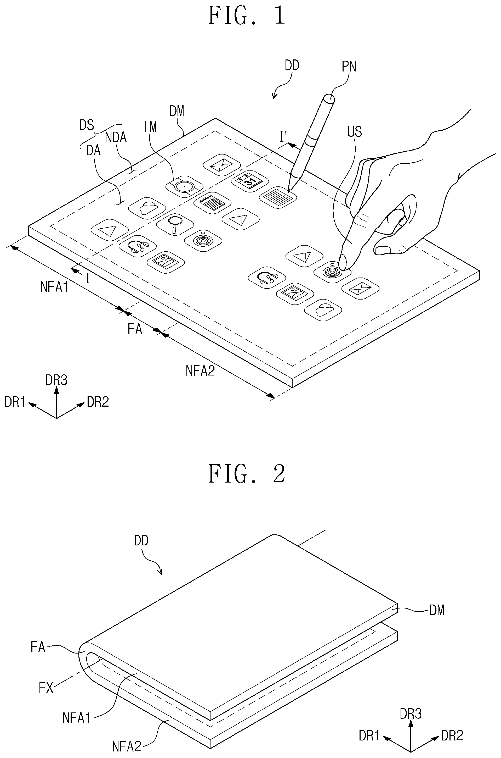
is a perspective view of a display device according to an embodiment of the inventive concept. is a perspective view illustrating a folded state of the display device of .
Referring to , a display device DD, according to an embodiment of the inventive concept, may include a display module DM and a pen PN disposed on the display module DM. The display module DM may have a rectangular shape having a pair of long sides extending in a first direction DR 1 and a pair of short sides extending in a second direction DR 2 crossing the first direction DR 1 . However, the embodiment of the inventive concept is not necessarily limited thereto. For example, the display module DM may have various shapes such as a circular shape, a polygonal shape, and the like. The display module DM may be a flexible display device.
Hereinafter, a direction that substantially perpendicularly crosses a plane defined by the first direction DR 1 and the second direction DR 2 is defined as a third direction DR 3 . Also, in this specification, the term “viewed from the plane” or “in a plan view” may be defined as a state when viewed in the third direction DR 3 .
The display module DM may include a folding area FA and a plurality of non-folding areas NFA 1 and NFA 2 . The non-folding areas NFA 1 and NFA 2 may include a first non-folding area NFA 1 and a second non-folding area NFA 2 . The folding area FA may be disposed between the first non-folding area NFA 1 and the second non-folding area NFA 2 . The folding area FA, the first non-folding area NFA 1 , and the second non-folding area NFA 2 may be arranged in the first direction DR 1 .
A top surface of the display module DM may be defined as a display surface DS and may have a plane defined by the first direction DR 1 and the second direction DR 2 . Images IM generated from the display module DM may be provided to a user through the display surface DS.
The display surface DS may include a display area DA and a non-display area NDA at least partially surrounding the display area DA. An image may be displayed on the display area DA, but might not be displayed on the non-display area NDA. The non-display area NDA may surround the display area DA and define an edge of the display module DM, which is printed with a predetermined color.
The display module DM may sense input applied from the outside of the display module DM. For example, the display module DM may sense a first input by a touch of an user US and a second input by a pen PN.
Referring to , the display device DD may be a folding-type (foldable) display device DD that is capable of being folded and/or unfolded to a noticeable extent without cracking or otherwise sustaining damage thereto. For example, the folding area FA may be bent with respect to a folding axis FX parallel to the second direction DR 2 , and thus, the display module DM may be folded. The folding axis may be defined as a short axis parallel to the short sides of the display module DM. However, the embodiment is not necessarily limited thereto. For example, the folding axis FX may be defined as a long axis parallel to the long sides of the display module DM, and the display module DM may be folded based on the folding axis FX defined as the long axis.
When folding the display module DM, the first non-folding area NFA 1 and the second non-folding areas NFA 2 may face each other, and the display module DM may be in-folded to prevent the display surface DS from being exposed to the outside. However, the embodiment is not necessarily limited thereto, and the display module DM may be out-folded so that the display surface DS of the display module is exposed to the outside and remain visible when in the folded state.
Although the folding display device DD has been described as an example, the embodiment is not necessarily limited thereto, and in an embodiment of the inventive concept, the display device DD may be a flat panel display device maintained in a flat state.
is a cross-sectional view taken along line I-I′ of .
Referring to , the display module DM may include an electronic panel EP, an impact absorption layer ISL, a panel protective layer PPL, a first conductive sheet CTS 1 , a second conductive sheet CTS 2 , a window WIN, a window protective layer WP, a hard coating layer HC, and first to sixth adhesive layers AL 1 to AL 6 .
The electronic panel EP may display an image, sense the above-described first and second inputs, and reduce reflectance of external light. The electronic panel EP may include a display panel, an input sensing part, and an antireflection layer, and constituents of the electronic panel EP will be described with reference to below.
The impact absorption layer ISL may be disposed on the electronic panel EP. The impact absorption layer ISL may be configured to protect the electronic panel EP by absorbing an external impact applied from the upper side of the display device DD toward the electronic panel EP. The impact absorption layer ISL may be manufactured in the form of a stretched film.
The impact absorption layer ISL may include a flexible plastic material. The flexible plastic material may be defined as a synthetic resin film. For example, the impact absorption layer ISL may include a flexible plastic material such as polyimide (PI) or polyethylene terephthalte (PET).
The panel protective layer PPL may be disposed under the electronic panel EP. The panel protective layer PPL may be configured to protect a lower portion of the electronic panel EP. The panel protective layer PPL may include a flexible plastic material. For example, the panel protective layer PPL may include polyethylene terephthalate (PET).
The first conductive sheet CTS 1 may be disposed under the panel protective layer PPL. The second conductive sheet CTS 2 may be disposed under the first conductive sheet CTS 1 . Each of the first conductive sheet CTS 1 and the second conductive sheet CTS 2 may include a metal.
The first conductive sheet CTS 1 may include a ferromagnetic material. For example, the first conductive sheet CTS 1 may be defined as a ferrite sheet including ferrite. The second conductive sheet CTS 2 may include a diamagnetic material. For example, the second conductive sheet CTS 2 may be defined as a copper sheet containing copper. The first and second conductive sheets CTS 1 and CTS 2 may shield an external magnetic field from being applied to the electronic panel EP under the display module DM.
The window WIN may be disposed on the impact absorption layer ISL. The window WIN may be configured to protect the electronic panel EP from external scratches. The window WIN may have optically transparent properties (e.g., may be transparent to visible light). The window WIN may include glass. However, the embodiment of the inventive concept is not necessarily limited thereto, and the window WIN may include a synthetic resin film.
The window WIN may has a single-layer or multi-layer structure. For example, the window WIN may include a plurality of plastic films bonded to each other by using an adhesive or include a glass substrate and a plastic film, which are bonded to each other by using an adhesive.
The window protective layer WP may be disposed on the window WIN. The window protective layer WP may include a flexible plastic material such as polyimide or polyethylene terephthalate. The hard coating layer HC may be disposed on a top surface of the window protective layer WP.
A printing layer PIT may be disposed on a bottom surface of the window protective layer WP. The printing layer PIT may have a black color, but the color of the printing layer PIT is not necessarily limited thereto. The printing layer PIT may be adjacent to an edge of the window protective layer WP. The printing layer PIT may overlap the non-display area NDA.
The first adhesive layer AL 1 may be disposed between the window protective layer WP and the window WIN. The window protective layer WP and the window WIN may be bonded to each other by the first adhesive layer AL 1 . The first adhesive layer AL 1 may cover the printing layer PIT.
The second adhesive layer AL 2 may be disposed between the window WIN and the impact absorption layer ISL. The window WIN and the impact absorption layer ISL may be bonded to each other by the second adhesive layer AL 2 .
The third adhesive layer AL 3 may be disposed between the impact absorption layer ISL and the electronic panel EP. The impact absorption layer ISL and the electronic panel EP may be bonded to each other by the third adhesive layer AL 3 .
A fourth adhesive layer AL 4 may be disposed between the electronic panel EP and the panel protective layer PPL. The electronic panel EP and the panel protective layer PPL may be bonded to each other by the fourth adhesive layer AL 4 .
A fifth adhesive layer AL 5 may be disposed between the panel protective layer PPL and the first conductive sheet CTS 1 . The panel protective layer PPL and the first conductive sheet CTS 1 may be bonded to each other by the fifth adhesive layer AL 5 .
A sixth adhesive layer AL 6 may be disposed between the first conductive sheet CTS 1 and the second conductive sheet CTS 2 . The first conductive sheet CTS 1 and the second conductive sheet CTS 2 may be bonded to each other by the sixth adhesive layer AL 6 .
Each of the first to sixth adhesive layers AL 1 and AL 6 may include a pressure sensitive adhesive (PSA) or an optically clear adhesive (OCA), but the type of adhesive is not necessarily limited thereto.
is a cross-sectional view illustrating the electronic panel having a configuration of an electronic panel of .
For example, illustrates a cross-sectional view of the electronic panel EP when viewed in the first direction DR 1 .
Referring to , the electronic panel EP may include a display panel DP, an input sensing part ISP disposed on the display panel DP, and an anti-reflection layer RPL disposed on the input sensing part ISP. The display panel DP may be a flexible display panel. For example, the display panel DP may include a flexible substrate and a plurality of elements disposed on the flexible substrate.
The display panel DP, according to an embodiment of the inventive concept, may be an emission type display panel, but is not necessarily limited thereto. For example, the display panel DP may be an organic light emitting diode (OLED) display panel or an inorganic light emitting display panel. An emission layer of the organic light emitting display panel may include an organic light emitting material. An emission layer of the inorganic light emitting display panel may include a quantum dot, a quantum rod, and the like. Hereinafter, the display panel DP is described as an organic light emitting diode display panel.
The input sensing part ISP may include a plurality of sensing electrodes (hereinafter, illustrated in ) for sensing the above-described first input in a capacitive manner. The input sensing part ISP may include a plurality of pen sensing electrodes (hereinafter, illustrated in ) for sensing the above-described second input using an electromagnetic method (or an electromagnetic resonance method). The input sensing part ISP may be directly disposed on the display panel DP when the electronic panel EP is manufactured.
When an external magnetic field is applied to the input sensing part ISP under the electronic panel EP, a sensing operation of the second input of the input sensing part ISP might not be normally performed. The above-described first and second conductive sheets CTS 1 and CTS 2 may shield the external magnetic field so as not to be applied to the input sensing part ISP from a lower side of the electronic panel EP.
The anti-reflection layer RPL may be disposed on the input sensing part ISP. The anti-reflection layer RPL may be directly disposed on the input sensing part ISP when the electronic panel EP is manufactured. The anti-reflection layer RPL may be defined as an external light anti-reflection film. The anti-reflection layer RPL may reduce reflectance of external light incident from the display device DD onto the display panel DP.
For example, the input sensing part ISP may be directly disposed on the display panel DP, and the anti-reflection layer RPL may be directly disposed on the input sensing part ISP, but the embodiment of the inventive concept is not necessarily limited thereto. For example, the input sensing part ISP may be separately manufactured and attached to the display panel DP using an adhesive layer, and the antireflection layer RPL may be separately manufactured and attached to the input sensing part ISP using an adhesive layer.
is a cross-sectional view illustrating a configuration of the display panel of .
For example, illustrates a cross-sectional view of the display panel DP when viewed in the first direction DR 1 .
Referring to , the display panel DP may include a substrate SUB, a circuit element layer DP-CL disposed on the substrate SUB, and a display element layer DP-OLED disposed on the circuit element layer DP-CL, and a thin film encapsulation layer TFE disposed on the display element layer DP-OLED.
The substrate SUB may include a display area DA and a non-display area NDA at least partially surrounding the display area DA. The substrate SUB may include a flexible plastic material such as polyimide (PI). The display element layer DP-OLED may be disposed on the display area DA.
A plurality of pixels may be disposed on the display area DA. Each of the pixels may include a light emitting element electrically connected to a transistor disposed on the circuit element layer DP-CL and disposed on the display element layer DP-OLED.
The thin film encapsulation layer TFE may be disposed on the circuit element layer DP-CL and may cover the display element layer DP-OLED. The thin film encapsulation layer TEF may include inorganic layers and an organic layer between the inorganic layers. The inorganic layers may be configured to protect the pixels from moisture and/or oxygen. The organic layer may be configured to protect the pixels from foreign substances such as dust particles. is a plan view of the display panel of .
Referring to , the display module DM may include a display panel DP, a scan driver SDV, a data driver DDV, a light emission driver EDV, and a plurality of first pads PD 1 .
The display panel DP may have a rectangular shape having a pair of long sides extending in the first direction DR 1 and a pair of short sides extending in the second direction DR 2 , but the shape of the display panel DP is not necessarily limited thereto. The display panel DP may include a display area DA and a non-display area NDA at least partially surrounding the display area DA.
The display panel DP may include a plurality of pixels PX, a plurality of scan lines SL 1 to SLm, a plurality of data lines DL 1 to DLn, a plurality of emission lines ELI to Elm, first and second control lines CSL 1 and CSL 2 , first and second power lines PL 1 and PL 2 , and connection lines CNL. Here, m and n are positive integers.
The pixels PX may be disposed on the display area DA. The scan driver SDV and the data driver DDV may be disposed on the non-display areas that are adjacent to the long sides of the display panel DP, respectively. The data driver DDV may be disposed on the non-display area NDA adjacent to one short side of the pair of short sides of the display panel DP. In a plan view, the data driver DDV may be adjacent to a lower end of the display panel DP.
The scan lines SL 1 to SLm may extend in the second direction DR 2 and be electrically connected to the pixels PX and the scan driver SDV. The data lines DL 1 to DLn may extend in the first direction DR 1 and be electrically connected to the pixels PX and the data driver DDV. The emission lines ELI to Elm may extend in the second direction DR 2 and be electrically connected to the pixels PX and the light emission driver EDV.
The first power line PL 1 may extend in the first direction DR 1 and be disposed on the non-display area NDA. The first power line PL 1 may be disposed between the display area DA and the light emission driver EDV.
The connection lines CNL may extend in the second direction DR 2 and may be arranged in the first direction DR 1 so as to be electrically connected to the first power line PL 1 and the pixels PX. The first voltage may be applied to the pixels PX through the first power line PL 1 and the connection lines CNL, which are electrically connected to each other.
The second power line PL 2 may be disposed on the non-display area NDA and may extend along the long sides of the display panel DP and another short side of the display panel DP on which the data driver DDV is not disposed. The second power line PL 2 may be disposed outside the scan driver SDV and the light emission driver EDV.
the second power line PL 2 may extend toward the display area DA and be electrically connected to the pixels PX. A second voltage having a level less than that of the first voltage may be applied to the pixels PX through the second power line PL 2 .
The first control line CSL 1 may be electrically connected to the scan driver SDV, and the first control line CSL 1 may extend toward the lower end of the display panel DP. The second control line CSL 2 may be electrically connected to the light emission driver EDV, and the second control line CSL 2 may extend toward the lower end of the display panel DP. The data driver DDV may be disposed between the first control line CSL 1 and the second control line CSL 2 .
The first pads PD 1 may be disposed on the non-display area NDA adjacent to a lower end of the display panel DP and may be closer to the lower end of the display panel DP than the data driver DDV. The data driver DDV, the first power line PL 1 , the second power line PL 2 , the first control line CSL 1 , and the second control line CSL 2 may be electrically connected to the first pads PD. The data lines DL 1 to DLn may be electrically connected to the data driver DDV, and the data driver DDV may be electrically connected to the first pads PD, which correspond to the data lines DL 1 to DLn.
The display device DD may further include a timing controller to control operations of the scan driver SDV, the data driver DDV, and the light emission driver EDV and a voltage generator to generate first and second voltages. The timing controller and the voltage generator may be electrically connected to the first pads PD 1 through the printed circuit board.
The scan driver SDV may generate a plurality of scan signals, and the scan signals may be applied to the pixels PX through the scan lines SL 1 to SLm. The data driver DDV may generate a plurality of data voltages, and the data voltages may be applied to the pixels PX through the data lines DL 1 to DLn. The light emission driver EDV may generate a plurality of emission signals, and the emission signals may be applied to the pixels PX through the emission lines Ell to ELm.
The pixels PX may receive the data voltages in response to the scan signals. The pixels PX may emit light having luminance corresponding the data voltages in response to the emission signals to display an image.
is a view illustrating an example of a cross-section of the electronic panel corresponding to one pixel of .
Referring to , the pixel PX may include a transistor TR and a light emitting element OLED. The light emitting element OLED may include a first electrode AE (or anode), a second electrode CE (or cathode), a hole control layer HCL, an electron control layer ECL, and an emission layer EML.
The transistor TR and the light emitting element OLED may be disposed on the substrate SUB. For example, one transistor TR is illustrated, but the pixel PX may include a plurality of transistors and at least one capacitor, which drive the light emitting element OLED.
The display area DA may include an emission area LA corresponding to each of the pixels PX and a non-emission area NLA at least partially surrounding the emission area LA. The light emitting element OLED may be disposed on the emission area LA.
A buffer layer BFL may be disposed on the substrate SUB, and the buffer layer BFL may be an inorganic layer. A semiconductor pattern may be disposed on the buffer layer BFL. The semiconductor pattern may include polysilicon, amorphous silicon, and/or metal oxide.
The semiconductor pattern may be doped with an N-type dopant or a P-type dopant. The semiconductor pattern may include a highly doped region and a lowly doped region. The highly doped region may have conductivity that is greater than that of the lowly doped region to serve as a source electrode and a drain electrode of the transistor TR. The lowly doped region may correspond to an active (or channel) of the transistor.
A source S, an active A, and a drain D of the transistor TR may be formed from the semiconductor pattern. An first insulating layer INS 1 may be disposed on the semiconductor pattern. The gate G of the transistor TR may be disposed on the first insulating layer INS 1 . A second insulating layer INS 2 may be disposed on the gate G. A third insulating layer INS 3 may be disposed on the second insulating layer INS 2 .
The connection electrode CNE may include a first connection electrode CNE 1 and a second connection electrode CNE 2 to connect the transistor TR to the light emitting element OLED. The first connection electrode CNE 1 may be disposed on the third insulating layer INS 3 and be electrically connected to the drain D through a first contact hole CH 1 defined in the first to third insulating layers INS 1 to INS 3 .
A fourth insulating layer INS 4 may be disposed on the first connection electrode CNE 1 . A fifth insulating layer INS 5 may be disposed on the fourth insulating layer INS 4 . The second connection electrode CNE 2 may be disposed on the fifth insulating layer INS 5 . The second connection electrode CNE 2 may be electrically connected to the first connection electrode CNE 1 through the second contact hole CH 2 defined in the fourth and fifth insulating layers INS 4 and INS 5 .
A sixth insulating layer INS 6 may be disposed on the second connection electrode CNE 2 . A layer provided from the buffer layer BFL to the sixth insulating layer INS 6 may be defined as the circuit element layer DP-CL. Each of the first insulating layer INS 1 to the sixth insulating layer INS 6 may be an inorganic layer or an organic layer.
The first electrode AE may be disposed on the sixth insulating layer INS 6 . The first electrode AE may be electrically connected to the second connection electrode CNE 2 through a third contact hole CH 3 defined in the sixth insulating layer INS 6 . A pixel defining layer PDL, in which an opening for exposing a predetermined portion of the first electrode AE is defined, may be disposed on the first electrode AE and the sixth insulating layer INS 6 .
The hole control layer HCL may be disposed on the first electrode AE and the pixel defining layer PDL. The hole control layer HCL may include a hole transport layer and a hole injection layer.
The emission layer EML may be disposed on the hole control layer HCL. The emission layer EML may be disposed on an area corresponding to the opening PX_OP. The emission layer EML may include an organic material and/or an inorganic material. The emission layer EML may emit one of red light, green light, and blue light.
The electronic control layer ECL may be disposed on the hole control layer HCL and may cover the emission layer EML. The charge control layer OL may include an electron transport layer and an electron injection layer. A hole control layer HCL and an electron control layer ECL may be commonly disposed on the emission area LA and the non-emission area NLA.
The second electrode CE may be disposed on the electronic control layer ECL. The second electrode CE may be commonly disposed in the pixels PX. The layer on which the light emitting element OLED is disposed may be defined as the display element layer DP-OLED.
The thin film encapsulation layer TFE may be disposed on the second electrode CE and may cover the pixel PX. The thin film encapsulation layer TFE may include a first encapsulation layer EN 1 disposed on the second electrode CE, a second encapsulation layer EN 2 disposed on the first encapsulation layer EN 1 , and a third encapsulation layer EN 3 disposed on the second encapsulation layer EN 2 .
Each of the first and third encapsulation layers EN 1 and EN 3 may include an inorganic insulating layer and may be configured to protect the pixel PX against moisture/oxygen. The second encapsulation layer EN 2 may include an organic insulating layer and may be configured to protect the pixel PX against foreign substances such as dust particles.
A first voltage may be applied to the first electrode AE through the transistor TR, and a second voltage having a level lower than that of the first voltage may be applied to the second electrode CE. Holes and electrons injected into the light emitting layer EML may be coupled to each other to form exciton. While the exciton may be transitioned to a ground state, the light emitting element OLED may emit light.
The input sensing part ISP may be disposed on the thin film encapsulation layer TFE. The input sensing part ISP may be manufactured directly on a top surface of the thin film encapsulation layer TFE.
A base layer BSL may be disposed on the thin film encapsulation layer TFE. The base layer BSL may include an inorganic insulating layer. At least one inorganic insulating layer may be provided on the thin film encapsulation layer TFE as the base layer BSL.
The input sensing part ISP may include a first conductive pattern CTL 1 and a second conductive pattern CTL 2 disposed on the first conductive pattern CTL 1 . The first conductive pattern CTL 1 may be disposed on the base layer BSL. An insulating layer TINS may be disposed on the base layer BSL and may cover the first conductive pattern CTL 1 . The insulating layer TINS may include an inorganic insulating layer or an organic insulating layer. The second conductive pattern CTL 2 may be disposed on the insulating layer TINS.
The first and second conductive patterns CTL 1 and CTL 2 may overlap the non-emission area NLA. The first and second conductive patterns CTL 1 and CTL 2 may be disposed on the non-emission area NLA between the emission areas LA and may have a mesh shape.
The first and second conductive patterns CTL 1 and CTL 2 may form sensing electrodes and pen sensing electrodes of the above-described input sensing part ISP. For example, the mesh-shaped first and second conductive patterns CTL 1 and CTL 2 may be separated from each other in a predetermined area to form the sensing electrodes and the pen sensing electrodes. A portion of the second conductive pattern CTL 2 may be electrically connected to the first conductive pattern CTL 1 .
An anti-reflection layer RPL may be disposed on the second conductive pattern CTL 2 . The anti-reflection layer RPL may include a black matrix BM and a plurality of color filters CF. The black matrix BM may overlap the non-emission area NLA, and the color filters CF may overlap the emission areas LA, respectively.
The black matrix BM may be disposed on the insulating layer TINS and may cover the second conductive pattern CTL 2 . An opening B_OP overlapping the emission area LA and the opening PX_OP may be defined in the black matrix BM. The black matrix BM may absorb and block light. A width of the opening B_OP may be greater than a width of the opening PX_OP.
The color filters CF may be disposed on the insulating layer TINS and the black matrix BM. The color filters CF may be respectively disposed in the openings B_OP. A planarization insulating layer PINS may be disposed on the color filters CF. The planarization insulating layer PINS may provide a flat (e.g., planar) top surface. The planarization insulating layer PINS may include an organic insulating layer.
When the external light traveling toward the display panel DP is reflected from the display panel DP and provided again to an external user, the user may visually recognize the external light, like a mirror. To prevent this phenomenon, for example, the anti-reflection layer RPL may include a plurality of color filters CF displaying the same color as the pixels PX of the display panel DP. The color filters CF may filter external light with the same colors as the pixels PX. In this case, the external light might not be visually recognized by the user.
is a plan view illustrating the input sensing part of . is an enlarged view illustrating a first area AA 1 of . is a view illustrating a first- 2 pen sensing electrode, a second- 2 pen sensing electrode, a dummy electrode, and first and second connection patterns, which are illustrated in .
Referring to , the input sensing part ISP may have a rectangular shape having a pair of long sides in a first direction DR 1 and a pair of short sides in a second direction DR 2 crossing the first direction DR 1 .
The input sensing part ISP may include a plurality of sensing electrodes SE 1 and SE 2 , a plurality of sensing lines TL and RL, a plurality of first- 1 and second- 1 pen sensing electrodes PSE 1 - 1 and PSE 2 - 1 , a plurality of pen sensing lines PSL 1 , PSL 2 , and PSL 3 - 1 to PSL 3 - 3 , and a plurality of second and third pads PD 2 and PD 3 . The sensing electrodes SE 1 and SE 2 , the sensing lines TL and RL, the first- 1 and second- 1 pen sensing electrodes PSE 1 - 1 and PSE 2 - 1 , the pen sensing lines PSL 1 , PSL 2 , and PSL 3 - 1 to PSL 3 - 3 , and the second and third pads PD 2 and PD 3 may be disposed on the above-described thin film encapsulation layer TFE.
A planar area of the input sensing part ISP may include an active area AA and a non-active area NAA at least partially surrounding the active area AA. When viewed in the plan view, the active area AA may overlap the display area DA, and the non-active area NAA may overlap the non-display area NDA.
The sensing electrodes SE 1 and SE 2 may be disposed on the active area AA, and the second and third pads PD 2 and PD 3 may be disposed on the non-active area NAA. The second pads PD 2 and the third pads PD 3 may be adjacent to a lower end of the input sensing part ISP when viewed from the plan view.
For example, the second pads PD 2 may be disposed adjacent to a left side of the input sensing part ISP, and the third pads PD 3 may be disposed adjacent to a right side of the input sensing part ISP. When viewed from the plan view, the first pads PD 1 illustrated in may be disposed between the second pads PD 2 and the third pads PD 3 .
The sensing electrodes SE 1 and SE 2 includes a plurality of first sensing electrodes SE 1 extending in the first direction DR 1 and arranged in the second direction DR 2 and a plurality of second sensing electrodes SE 2 extending in the second direction DR 2 and arranged in the first direction DR 1 . The second sensing electrodes SE 2 may be electrically insulated from the first sensing electrodes SE 1 and may cross each other. The first and second sensing electrodes SE 1 and SE 2 may be used to sense the above-described first input.
The sensing lines TL and RL may be electrically connected to ends of the first and second sensing electrodes SE 1 and SE 2 and extend on the inactive area NAA so as to be electrically connected to the second and third pads PD 2 and PD 3 . The sensing lines TL and RL may include a plurality of first sensing lines TL electrically connected to the first sensing electrodes SE 1 and a plurality of second sensing lines RL electrically connected to the second sensing electrodes SE 2 .
For example, when viewed from the plan view, the first sensing lines TL may be disposed on the non-active area NAA adjacent to a lower side of the active area AA. Also, when viewed from the plan view, the second sensing lines RL may be disposed on the non-active area NAA adjacent to left and right sides of the active area AA.
The first sensing lines TL may be electrically connected to lower ends of the first sensing electrodes SE 1 . The first sensing lines TL may extend to the non-active area NAA and be electrically connected to the corresponding second and third pads PD 2 and PD 3 .
The input sensing part ISP may be divided into a left portion and a right portion based on a center thereof in the second direction DR 2 . The first sensing lines TL electrically connected to the first sensing electrodes SE 1 disposed at the left portion may be electrically connected to the corresponding second pads PD 2 . The first sensing lines TL electrically connected to the first sensing electrodes SE 1 disposed on the right portion may be electrically connected to the corresponding third pads PD 3 .
The second sensing lines RL may be electrically connected to left ends or right ends of the second sensing electrodes SE 2 . The second sensing lines RL may extend to the non-active area NAA and be electrically connected to the corresponding second and third pads PD 2 and PD 3 .
The input sensing part ISP may be divided into a lower portion and an upper portion based on a center thereof in the first direction DR 1 . The second sensing lines RL disposed at the lower portion of the input sensing part ISP may be electrically connected to the left ends of the second sensing electrodes SE 2 disposed at the lower portion of the input sensing part ISP. The second sensing lines RL disposed at the upper portion of the input sensing part ISP may be electrically connected to the right ends of the second sensing electrodes SE 2 disposed at the upper portion of the input sensing part ISP.
The second sensing lines RL disposed at the lower portion of the input sensing part ISP may be disposed on the non-active area NAA adjacent to the left side of the active area AA. The second sensing lines RL disposed at the lower portion the input sensing part ISP may extend toward the lower end of the input sensing part ISP and be electrically connected to the corresponding second pads PD 2 .
The second sensing lines RL disposed at the upper portion of the input sensing part ISP may be disposed on the non-active area NAA adjacent to the right side of the active area AA. The second sensing lines RL disposed at the upper portion of the input sensing part ISP may extend toward the lower end of the input sensing part ISP and be electrically connected to the corresponding third pads PD 3 .
Each of the first sensing electrodes SE 1 may include a first- 1 sensing electrode SE 1 - 1 and a first- 2 sensing electrode SE 1 - 2 extending in the first direction DR 1 and spaced apart from each other in the second direction DR 2 . The first- 1 sensing electrode SE 1 - 1 and the first- 2 sensing electrode SE 1 - 2 may have shapes symmetrical to each other in the second direction DR 2 .
In each of the first sensing electrodes SE 1 , a lower end of the first- 1 sensing electrode SE 1 - 1 and a lower end of the first- 2 sensing electrode SE 1 - 2 may be integrated with each other so as to be electrically connected to the corresponding first sensing line TL of the first sensing lines TL. In each of the first sensing electrodes SE 1 , an upper end of the first- 1 sensing electrode SE 1 - 1 and an upper end of the first- 2 sensing electrode SE 1 - 2 may be separated from each other so as not to be electrically connected to each other.
Each of the second sensing electrodes SE 2 may include a second- 1 sensing electrode SE 2 - 1 and a second- 2 sensing electrode SE 2 - 2 extending in the second direction DR 2 and spaced apart from each other in the first direction DR 1 . The second- 1 sensing electrode SE 2 - 1 and the second- 2 sensing electrode SE 2 - 2 may have symmetrical shapes in the first direction DR 1 .
In each of the second sensing electrodes SE 2 disposed at the lower portion of the input sensing part ISP, a left end of the second- 1 sensing electrode SE 2 - 1 and a left end of the second- 2 nd sensing electrode SE 2 - 2 may be integrated with each other so as to be electrically connected to the corresponding second sensing line RL of the second sensing lines RL. In each of the second sensing electrodes SE 2 disposed at the lower portion of the input sensing part ISP, a right end of the second- 1 sensing electrode SE 2 - 1 and a right end of the second- 2 nd sensing electrode SE 2 - 2 may be separated from each other so as not to be electrically connected to each other.
In each of the second sensing electrodes SE 2 disposed at the upper portion of the input sensing part ISP, a right end of the second- 1 sensing electrode SE 2 - 1 and a right end of the second- 2 sensing electrode SE 2 - 2 may be integrated with each other so as to be electrically connected to the corresponding second sensing line RL of the second sensing lines RL. In each of the second sensing electrodes SE 2 disposed at the upper portion the input sensing part ISP, a left end of the second- 1 sensing electrode SE 2 - 1 and a left end of the second- 2 sensing electrode SE 2 - 2 may be separated from each other so as not to be electrically connected to each other.
The first- 1 and second- 1 pen sensing electrodes PSE 1 - 1 and PSE 2 - 1 may be disposed on the active area AA. The pen sensing lines PSL 1 , PSL 2 , and PSL 3 - 1 to PSL 3 - 3 may be electrically connected to the first- 1 and second- 1 pen sensing electrodes PSE 1 - 1 and PSE 2 - 1 , may extend to the inactive area, and may be electrically connected to the corresponding second and third pads PD 2 and PD 3 .
A sensing IC for controlling the input sensing part ISP may be electrically connected to the second and third pads PD 2 and PD 3 through a printed circuit board.
The plurality of first- 1 pen sensing electrodes PSE 1 - 1 may extend in the first direction DR 1 and be arranged in the second direction DR 2 . The plurality of the second- 1 pen sensing electrodes PSE 2 - 1 may extend in the second direction DR 2 and be arranged in the first direction DR 1 . The first- 1 and second- 1 pen sensing electrodes PSE 1 - 1 and PSE 2 - 1 may be used to sense the above-described second input.
The first- 1 pen sensing electrodes PSE 1 - 1 may be adjacent to the first sensing electrodes SE 1 , respectively. The first- 1 pen sensing electrodes PSE 1 - 1 may be electrically insulated from and spaced apart from the first sensing electrodes SE 1 . The second- 1 pen sensing electrodes PSE 2 - 1 may be adjacent to the second sensing electrodes SE 2 , respectively. The second- 1 pen sensing electrodes PSE 2 - 1 may be electrically insulated from and spaced apart from the second sensing electrodes SE 2 .
The first- 1 pen sensing electrodes PSE 1 - 1 may extend to be electrically insulated from and to cross the second sensing electrodes SE 2 . The second- 1 pen sensing electrodes PSE 2 - 1 may extend to be electrically insulated from and to cross the first- 1 pen sensing electrodes PSE 1 - 1 . The second- 1 pen sensing electrodes PSE 2 - 1 may extend to be electrically insulated from and to cross the first sensing electrodes SE 1 .
Each of the first- 1 pen sensing electrodes PSE 1 - 1 may be disposed between the first- 1 sensing electrode SE 1 - 1 and the first- 2 sensing electrode SE 1 - 2 of the corresponding first sensing electrode SE 1 of the first sensing electrodes SE 1 . Each of the second- 1 pen sensing electrodes PSE 2 - 1 may be disposed between the second- 1 sensing electrode SE 2 - 1 and the second- 2 sensing electrode SE 2 - 2 of the corresponding second sensing electrode SE 2 of the second sensing electrodes SE 2 .
The first- 1 pen sensing electrodes PSE 1 - 1 may be disposed on the same layer as the first sensing electrodes SE 1 . The second- 1 pen sensing electrodes PSE 2 - 1 may be disposed on the same layer as the second sensing electrodes SE 2 . Thus, the first- 1 and second- 1 pen sensing electrodes PSE 1 - 1 and PSE 2 - 1 may be disposed on the same layer as the first and second sensing electrodes SE 1 and SE 2 .
Upper ends of the first- 1 pen sensing electrodes PSE 1 - 1 may be electrically connected to each other. Lower ends of the first- 1 pen sensing electrodes PSE 1 - 1 may be electrically connected in a pair to each other. Left ends of the second- 1 pen sensing electrodes PSE 2 - 1 disposed on the upper portion of the input sensing part ISP may be electrically connected to each other. Right ends of the second- 1 pen sensing electrodes PSE 2 - 1 disposed on the lower portion of the input sensing part ISP may be electrically connected to each other.
Right ends of the second- 1 pen sensing electrodes PSE 2 - 1 disposed on the upper portion of the input sensing part ISP might not be separated from each other so as not to be electrically connected to each other. Left ends of the second- 1 pen sensing electrodes PSE 2 - 1 disposed on the lower portion of the input sensing part ISP might not be separated from each other so as not to be electrically connected to each other.
The pen sensing lines PSL 1 , PSL 2 , and PSL 3 - 1 to PSL 3 - 3 may include a plurality of first pen sensing lines PSL 1 , a plurality of second pen sensing lines PSL 2 , and a plurality of third- 1 , third- 2 and third- 3 pen sensing lines PSL 3 - 1 , PSL 3 - 2 , and PSL 3 - 3 . The first pen sensing lines PSL 1 and the third- 1 , third- 2 , and third- 3 pen sensing lines PSL 3 - 1 , PSL 3 - 2 , and PSL 3 - 3 may be electrically connected to the first- 1 pen sensing electrodes PSE 1 - 1 . The second pen sensing lines PSL 2 may be electrically connected to the second- 1 pen sensing electrodes PSE 2 - 1 .
The pair of first- 1 pen sensing electrodes PSE 1 - 1 of which the lower ends are electrically connected to each other may be electrically connected to the corresponding first pen sensing line PSL 1 of the first pen sensing lines PSL 1 . The upper ends of the first- 1 pen sensing electrodes PSE 1 - 1 may be electrically connected to the third- 1 pen sensing line PSL 3 - 1 extending in the second direction DR 2 .
The third- 2 pen sensing line PSL 3 - 2 and the third- 3 pen sensing line PSL 3 - 3 may extend from both ends of the third- 1 pen sensing line PSL 3 - 1 in the first direction DR 1 . The third- 2 pen sensing line PSL 3 - 2 may be disposed at the left side of the input sensing part ISP, extend toward the lower end of the input sensing part ISP, and be electrically connected to the corresponding second pad PD 2 . The third- 3 pen sensing line PSL 3 - 3 may be disposed on the right side of the input sensing part ISP, extend toward the lower end of the input sensing part ISP, and be electrically connected to the corresponding third pad PD 3 .
The left ends of the second- 1 pen sensing electrodes PSE 2 - 1 disposed on the upper portion of the input sensing part ISP may be electrically connected to the corresponding second pen sensing lines PSL 2 of the second pen sensing lines PSL 2 . The second pen sensing line PSL 2 electrically connected to the second- 1 pen sensing electrodes PSE 2 - 1 disposed on the upper portion of the input sensing part ISP may be disposed on the left side of the input sensing part ISP so as to be electrically connected to the corresponding second pad PD 2 .
The right ends of the second- 1 pen sensing electrodes PSE 2 - 1 disposed on the lower portion of the input sensing part ISP may be electrically connected to the corresponding second pen sensing lines PSL 2 of the second pen sensing lines PSL 2 . The second pen sensing line PSL 2 electrically connected to the second- 1 pen sensing electrodes PSE 2 - 1 disposed on the lower portion of the input sensing part ISP may be disposed at the right side of the input sensing part ISP so as to be electrically connected to the corresponding the third pad PD 3 .
For example, the input sensing part ISP may be driven in time division to be driven in a first sensing section and a second sensing section. The first sensing section and the second sensing section may be repeated. In the first sensing section, the first and second sensing electrodes SE 1 and SE 2 may be driven to sense a touch of the user US. In the second sensing section, a touch of the pen PN may be sensed by the first- 1 and second- 1 pen sensing electrodes PSE 1 - 1 and PSE 2 - 1 . An operation of sensing the touch of the pen PN will be described in detail below.
Since the touch of the user US and the touch of the pen PN are performed by the same input sensing part ISP, two input devices such as a touch panel and a digitizer might not be used to reduce a thickness of the display device DD.
For example, although six first- 1 pen sensing electrodes PSE 1 - 1 and eight second- 1 pen sensing electrodes PSE 2 - 1 are illustrated, but in practice, the input sensing part ISP may include more first- 1 pen sensing electrodes PSE 1 - 1 and second- 1 pen sensing electrodes PSE 2 - 1 .
Referring to , each of the first- 1 and first- 2 sensing electrodes SE 1 - 1 and SE 1 - 2 may include a plurality of first sensing parts SP 1 arranged in a first direction DR 1 and a plurality of first extension patterns EP 1 disposed between the first sensing parts SP 1 and may extend from the first sensing parts SP 1 in the first direction DR 1 .
Each of the first sensing parts SP 1 may have a bent shape. For example, the first sensing parts SP 1 of the first- 1 sensing electrode SE 1 - 1 and the first sensing parts SP 1 of the first- 2 sensing electrode SE 1 - 2 may be bent toward the outside.
In each of the first- 1 and first- 2 sensing electrodes SE 1 - 1 and SE 1 - 2 , the first extension patterns EP 1 may be integrated with the first sensing parts SP 1 . Each of the extension patterns EP may be disposed between two first sensing parts SP 1 adjacent to each other in the first direction DR 1 and may extend from the two first sensing part SP 1 .
Each of the second- 1 and second- 2 sensing electrodes SE 2 - 1 and SE 2 - 2 may include a plurality of second sensing parts SP 2 arranged in the second direction DR 2 and a plurality of first connection patterns CP 1 disposed between the plurality of second sensing parts SP 2 to connect the second sensing parts SP 2 .
Each of The second sensing parts SP 2 may have a bent shape. For example, the second sensing parts SP 2 of the second- 1 sensing electrode SE 2 - 1 and the second sensing parts SP 2 of the second- 2 sensing electrode SE 2 - 2 may be bent toward the outside.
The first connection patterns CP 1 may extend in the second direction DR 2 and be electrically connected to the second sensing parts SP 2 . The second sensing parts SP 2 may be electrically connected to each other through the first connection patterns CP 1 . When viewed in the plan view, the first connection patterns CP 1 may cross the first extension patterns EP 1 . The first connection patterns CP 1 may be electrically insulated from the first extension patterns EP 1 .
Each of the first connection patterns CP 1 may be disposed between two second sensing parts SP 2 adjacent to each other in the second direction DR 2 to connect the two second sensing parts SP 2 . An insulating layer may be disposed between the first connection patterns CP 1 and the second sensing parts SP 2 , and the first connection patterns CP 1 may be electrically connected to the second sensing parts SP 2 through first contact holes T-CH 1 defined in the insulating layer.
The first sensing parts SP 1 and the second sensing parts SP 2 might not overlap each other and be spaced apart from each other so as to be alternately arranged with respect to each other. Each of the first sensing parts SP 1 and the second sensing parts SP 2 may have electrostatic capacity.
The first and second sensing parts SP 1 and SP 2 and the first extension patterns EP 1 may be disposed on the same layer. The first connection patterns CP 1 may be disposed on a layer that is different from that on which the first and second sensing parts SP 1 and SP 2 and the first extension patterns EP 1 are disposed. The first connection patterns CP 1 may be disposed below the first and second sensing parts SP 1 and SP 2 and the first extension patterns EP 1 .
Each of the first- 1 pen sensing electrodes PSE 1 - 1 may include a plurality of first pen sensing parts PSP 1 arranged in the first direction DR 1 and a plurality of second extension patterns EP 2 extending from the first pen sensing parts PSP 1 in the first direction DR 1 .
Each of the first pen sensing parts PSP 1 may have a diamond shape, but the shape of each of the first pen sensing parts PSP 1 is not necessarily limited thereto. The second extension patterns EP 2 may be integrated with the first pen sensing parts PSP 1 . Each of the second extension patterns EP 2 may be disposed between two first pen sensing parts PSP 1 adjacent to each other in the first direction DR 1 and may extend from the two first pen sensing parts PSP 1 .
Each of the second- 1 pen sensing electrodes PSE 2 - 1 may include a plurality of second pen sensing parts PSP 2 arranged in the second direction DR 2 and a plurality of second connection patterns CP 2 connecting the second pen sensing parts PSP 2 .
Each of the second pen sensing parts PSP 2 may have a diamond shape, but the shape of each of the second pen sensing parts PSP 2 is not necessarily limited thereto. The second connection patterns CP 2 may extend in the second direction DR 2 , be disposed between the second pen sensing parts PSP 2 , and be electrically connected to the second pen sensing parts PSP 2 . The second pen sensing parts PSP 2 may be electrically connected to each other through the second connection patterns CP 2 .
Each of the second connection patterns CP 2 may be disposed between two second pen sensing parts PSP 2 adjacent to each other in the second direction DR 2 to connect the two second pen sensing parts PSP 2 . An insulating layer is disposed between the second connection patterns CP 2 and the second pen sensing parts PSP 2 , and the second connection patterns CP 2 may be electrically connected to the second pen sensing parts through a second contact holes T-CH 2 defined in the insulating layer.
Each of the second- 1 pen sensing electrodes PSE 2 - 1 may include dummy extensions DEP extending from the second pen sensing parts PSP 2 in the second direction. The second connection patterns CP 2 may be electrically connected to the dummy extensions DEP through the second contact holes T-CH 2 .
When viewed in the plan view, the first and second extension patterns EP 1 and EP 2 may extend to cross the first and second connection patterns CP 1 and CP 2 . The first and second extension patterns EP 1 and EP 2 may be electrically insulated from the first and second connection patterns CP 1 and CP 2 .
The first pen sensing parts PSP 1 , the second pen sensing parts PSP 2 , and the second extension patterns EP 2 may be disposed on the same layer as the first and second sensing parts SP 1 and SP 2 and the first extension patterns EP 1 . The second connection patterns CP 2 may be disposed on the same layer as the first connection patterns CP 1 . Thus, the first and second connection patterns CP 1 and CP 2 may be disposed below the first and second sensing parts SP 1 and SP 2 , the first and second pen sensing parts PSP 1 and PSP 2 , and the first and second extension patterns EP 1 and EP 2 .
The lower ends of the pair of first- 1 pen sensing electrodes PSE 1 - 1 may be electrically connected by the corresponding third connection pattern CP 3 of the third connection patterns CP 3 illustrated in . The third connection patterns CP 3 may be disposed on the same layer as the first and second connection patterns CP 1 and CP 2 . For example, the third connection patterns CP 3 may be disposed below the first- 1 pen sensing electrodes PSE 1 - 1 .
In , the first sensing lines TL and the third connection patterns CP 3 may be electrically insulated from each other and may extend to cross each other. For example, the first sensing lines TL may be disposed on the same layer as the first sensing parts SP 1 adjacent to the lower side of the active area AA and may extend from the first sensing parts SP 1 .
The third connection patterns CP 3 may be disposed below the first sensing lines TL and extend to cross the first sensing lines TL. An insulating layer may be disposed between the third connection patterns CP 3 and the first sensing lines TL. The first pen sensing lines PSL 1 may be disposed on the same layer as the third connection patterns CP 3 and may extend from the third connection patterns CP 3 . An insulating layer may be disposed between the first sensing lines TL and the first pen sensing lines PSL 1 .
Referring to , the input sensing part ISP may have a rectangular shape with a pair of long sides extending in the first direction DR 1 and a pair of short sides extending in the second direction DR 2 . Thus, the first sensing electrodes SE 1 may be longer than the second sensing electrodes SE 2 . In addition, the first- 1 pen sensing electrodes PSE 1 - 1 may be longer than the second- 1 pen sensing electrodes PSE 2 - 1 .
Resistance may be proportional to a length of the conductor. The resistance depending on the length of the conductor may be defined as line resistance. Thus, line resistance of the first sensing electrodes SE 1 may be greater than line resistance of the second sensing electrodes SE 2 . In addition, line resistance of the first- 1 pen sensing electrodes PSE 1 - 1 may be greater than line resistance of the second- 1 pen sensing electrodes PSE 2 - 1 .
The first and second connection patterns CP 1 and CP 2 may be defined as bridges. When the conductors are electrically connected by the bridges disposed on a layer that is different from that on which the conductors are disposed, resistance of each of electrodes provided as the conductors and bridges may increase.
In an embodiment of the inventive concept, the connection patterns may be used for the first sensing electrodes SE 1 and the first- 1 pen sensing electrodes PSE 1 - 1 , and the extension patterns may be used for the second sensing electrodes SE 2 and the second- 1 pen sensing electrodes PSE 2 - 1 . For example, the connection patterns disposed below the first sensing parts SP 1 and the first pen sensing parts PSP 1 may connect the first sensing parts SP 1 to the first pen sensing parts PSP 1 . In addition, the extension patterns integrated with the second sensing parts SP 2 and the second pen sensing parts PSP 2 may extend from the second sensing parts SP 2 and the second pen sensing parts PSP 2 .
When the connection patterns are used for the first sensing electrodes SE 1 and the first- 1 pen sensing electrodes PSE 1 - 1 , which are provided to be longer and thus have higher line resistance, line resistance of the first sensing electrodes SE 1 and the first- 1 pen sensing electrodes PSE 1 - 1 may increase. Thus, in the embodiment of the inventive concept, the first and second connection patterns CP 1 and CP 2 may be used for the second sensing electrodes SE 2 and the second- 1 pen sensing electrodes PSE 2 - 1 , each of which has a smaller length and relatively low line resistance.
Referring to , the input sensing part ISP may include a plurality of first- 2 pen sensing electrodes PSE 1 - 2 , a plurality of second- 2 pen sensing electrodes PSE 2 - 2 , and a plurality of dummy electrodes DME. For example, the first- 2 pen sensing electrodes, the second- 2 pen sensing electrodes PSE 2 - 2 , and the dummy electrodes DME overlapping the first and second sensing electrodes SE 1 and SE 2 and the first- 1 and the second- 1 pen sensing electrodes PSE 1 - 1 and PSE 2 - 1 are illustrated as dotted lines in .
Referring to , the first- 2 pen sensing electrodes PSE 1 - 2 may be disposed on a layer that is different from that on which the first- 1 pen sensing electrode PSE 1 - 1 is disposed. For example, the first- 2 pen sensing electrodes PSE 1 - 2 may be disposed under the first- 1 pen sensing electrode PSE 1 - 1 . The first- 2 pen sensing electrodes PSE 1 - 2 may be disposed on a layer that is different from that on which the first sensing electrode SE 1 is disposed. For example, the first- 2 pen sensing electrodes PSE 1 - 2 may be disposed below the first sensing electrode SE 1 .
The first- 2 pen sensing electrodes PSE 1 - 2 may be disposed below the first sensing parts SP 1 , the first pen sensing parts PSP 1 , and the first and second extension patterns EP 1 and EP 2 . The first- 2 pen sensing electrodes PSE 1 - 2 may be disposed on the same layer as the first and second connection patterns CP 1 and CP 2 .
When viewed in the plan view, the first- 2 pen sensing electrodes PSE 1 - 2 may overlap a portion of the first- 1 pen sensing electrode PSE 1 - 1 and a portion of the first sensing electrode SE 1 . For example, when viewed in the plan view, the first- 2 pen sensing electrodes PSE 1 - 2 may overlap the first pen sensing parts PSP 1 , respectively. The first- 2 pen sensing electrodes PSE 1 - 2 may overlap portions of the second extension patterns EP 2 . The first- 2 pen sensing electrodes PSE 1 - 2 may overlap portions of the first sensing parts SP 1 .
An area of each of the first- 2 pen sensing electrodes PSE 1 - 2 overlapping the first sensing parts SP 1 shown in may be illustrated as an example and may be adjusted variously. For example, when viewed in the plan view, the first- 2 pen sensing electrodes PSE 1 - 2 may overlap the whole of the first sensing parts SP 1 .
The first- 2 pen sensing electrodes PSE 1 - 2 may be electrically connected to the first- 1 pen sensing electrode PSE 1 - 1 through the first contact holes P-CH 1 . The first contact holes P-CH 1 may be defined in an insulating layer disposed between the first- 1 pen sensing electrode PSE 1 - 1 and the first- 2 pen sensing electrode PSE 1 - 2 . When viewed in the plan view, the first contact holes P-CH 1 may overlap the second extension patterns EP 2 .
The second- 2 pen sensing electrodes PSE 2 - 2 may be disposed on a layer that is different from that on which the second- 1 pen sensing electrode PSE 2 - 1 is disposed. For example, the second- 2 pen sensing electrodes PSE 2 - 2 may be disposed below the second pen sensing parts PSP 2 of the second- 1 pen sensing electrode PSE 2 - 1 . The second- 2 pen sensing electrodes PSE 2 - 2 may be disposed on a layer that is different from on which the second sensing electrode SE 2 is disposed. For example, the second- 2 pen sensing electrodes PSE 2 - 2 may be disposed below the second sensing parts SP 2 of the second sensing electrode SE 2 .
The second- 2 pen sensing electrodes PSE 2 - 2 may be disposed below the first and second sensing parts SP 1 and SP 2 , the first and second pen sensing parts PSP 1 and PSP 2 , and the first and second extension patterns EP 1 and EP 2 . The second- 2 pen sensing electrodes PSE 2 - 2 may be disposed on the same layer as the first- 2 pen sensing electrodes PSE 1 - 2 and the first and second connection patterns CP 1 and CP 2 .
When viewed in the plan view, the second- 2 pen sensing electrodes PSE 2 - 2 may overlap portions of the second- 1 pen sensing electrode PSE 2 - 1 and portions of the second sensing electrode SE 2 . For example, when viewed in the plan view, the second- 2 pen sensing electrodes PSE 2 - 2 may overlap the second pen sensing parts PSP 2 , respectively. The second- 2 pen sensing electrodes PSE 2 - 2 may overlap portions of the dummy extensions DEP. The second- 2 pen sensing electrodes PSE 2 - 2 may overlap portions of the second sensing parts SP 2 .
An area of each of the second- 2 pen sensing electrodes PSE 2 - 2 overlapping the second sensing parts SP 2 shown in may be illustrated as an example and may be adjusted variously. For example, when viewed in the plan view, the second- 2 pen sensing electrodes PSE 2 - 2 may overlap the whole of the second sensing parts SP 2 except for the portions electrically connected to the second connection patterns CP 2 .
The second- 2 pen sensing electrodes PSE 2 - 2 may be electrically connected to the second- 1 pen sensing electrode PSE 2 - 1 through the second contact holes P-CH 2 . The second contact holes P-CH 2 may be defined in an insulating layer disposed between the second- 1 pen sensing electrode PSE 2 - 1 and the second- 2 pen sensing electrode PSE 2 - 2 . When viewed in the plan view, the second contact holes P-CH 2 may overlap the dummy extensions DEP.
When viewed in the plan view, portions of the first- 2 pen sensing electrodes PSE 1 - 2 overlapping the first sensing electrode SE 1 may be defined as first overlapping portions OVAL The first overlapping portions OVA 1 may be defined as portions of the first- 2 pen sensing electrodes PSE 1 - 2 overlapping the first sensing portions SP 1 .
When viewed in the plan view, portions of the second- 2 pen sensing electrodes PSE 2 - 2 overlapping the second sensing electrode SE 2 may be defined as second overlapping portions OVA 2 . The second overlapping parts OVA 2 may be defined as portions of the second- 2 pen sensing electrodes PSE 2 - 2 overlapping the second sensing parts SP 2 . For example, the first overlapping portions OVA 1 may have the same area as the second overlapping portions OVA 2 .
The dummy electrodes DME may at least partially surround the first- 2 pen sensing electrodes PSE 1 - 2 . In addition, the dummy electrodes DME may at least partially surround the second- 2 pen sensing electrodes PSE 2 - 2 . The dummy electrodes DME may be disposed on the same layer as the first and second connection patterns CP 1 and CP 2 and the first- 2 and second- 2 pen sensing electrodes PSE 1 - 2 and PSE 2 - 2 .
The dummy electrodes DME may overlap a portion of the first sensing electrode SE 1 and a portion of the second sensing electrode SE 2 . For example, the dummy electrodes DME may overlap portions of the first sensing parts SP 1 and portions of the second sensing parts SP 2 .
When the dummy electrodes DME are not disposed at least partially surrounding the first- 2 and second- 2 pen sensing electrodes PSE 1 - 2 and PSE 2 - 2 , shapes of the first- 2 and second- 2 pen sensing electrodes PSE 1 - 2 and PSE 2 - 2 may be visually recognized to the outside (e.g., may be seen by a user). For example, when separate patterns are not disposed at least partially surrounding the first- 2 and second- 2 pen sensing electrodes PSE 1 - 2 and PSE 2 - 2 , but only the first- 2 and second- 2 pen sensing electrodes PSE 1 - 2 and PSE 2 - 2 are disposed, the shapes of the first- 2 and second- 2 pen sensing electrodes PSE 1 - 2 and PSE 2 - 2 may be well visually recognized from the outside.
However, in an embodiment of the inventive concept, when the dummy electrodes DME are additionally disposed adjacent to the first- 2 and second- 2 pen sensing electrodes PSE 1 - 2 and PSE 2 - 2 , the first- 2 and second- 2 pen sensing electrodes PSE 1 - 2 and PSE 2 - 2 might not be well visually recognized from the outside.
is a view illustrating detailed shapes of the first- 2 pen sensing electrode and the dummy electrode, which are illustrated on a second area AA 2 of .
Referring to , 10 , and 11 , in an embodiment of the inventive concept, each of the electrodes of the input sensing part ISP may have a mesh shape. For example, each of the first- 2 pen sensing electrode PSE 1 - 2 and the dummy electrodes DME adjacent to the first- 2 pen sensing electrode PSE 1 - 2 may have a mesh shape.
If the dummy electrodes DME are omitted, the first- 2 pen sensing electrodes PSE 1 - 2 may be more well visually recognized. However, since the dummy electrodes DME having the similar pattern are disposed adjacent to the first- 2 pen sensing electrode PSE 1 - 2 , the first- 2 pen sensing electrode PSE 1 - 2 and the dummy electrodes DME may overall look like the mesh pattern. For example, the shape of the first- 2 pen sensing electrode PSE 1 - 2 might not be clearly visibly recognized to the outside.
For example, although the mesh shape of the first- 2 pen sensing electrodes PSE 1 - 2 and the dummy electrodes DME are illustrated, all the first and second sensing electrodes SE 1 and SE 2 , the first and second sensing electrodes SE 1 and SE 2 , the first- 1 and first- 2 pen sensing electrodes PSE 1 - 1 and PSE 1 - 2 , the first- 2 and second- 2 pen sensing electrodes PSE 1 - 2 and PSE 2 - 2 , and the dummy electrodes DME may have the mesh shape illustrated in .
Each of the first- 2 pen sensing electrode PSE 1 - 2 and the dummy electrodes DME may include a plurality of first branch portions BP 1 extending in a first diagonal direction DDR 1 and a plurality of second branch parts BP 2 extending in a second diagonal direction DDR 2 .
The first diagonal direction DDR 1 may be defined as a direction crossing the first and second directions DR 1 and DR 2 on a plane defined by the first and second directions DR 1 and DR 2 . The second diagonal direction DDR 2 may be defined as a direction crossing the first diagonal direction DDR 1 and the first and second directions DR 1 and DR 2 on the plane defined by the first and second directions DR 1 and DR 2 .
The first and second branch portions BP 1 and BP 2 may cross each other and be integrated with each other. The mesh shape of the first- 2 pen sensing electrodes PSE 1 - 2 and the dummy electrodes DME may be defined by the first and second branch portions BP 1 and BP 2 .
Diamond-shaped openings T-OP may be defined by the first and second branch portions BP 1 and BP 2 . The emission areas LA of the above-described pixels PX may be respectively disposed on the openings T-OP. Thus, the first and second branch portions BP 1 and BP 2 may overlap the non-emission area NLA. For example, the first and second sensing electrodes SE 1 and SE 2 , the first- 1 and first- 2 pen sensing electrodes PSE 1 - 1 and PSE 1 - 2 , the first- 2 and second- 2 pen sensing electrodes PSE 1 - 2 and PSE 2 - 2 , and the dummy electrodes DME may overlap the non-emission area NLA.
Since the first and second branch portions BP 1 and BP 2 are disposed on the non-emission area NLA, light generated from the light emitting elements OLED of the pixels PX may be normally emitted without being affected by the first and second sensing electrodes SE 1 and SE 2 , the first- 1 and first- 2 pen sensing electrodes PSE 1 - 1 and PSE 1 - 2 , the first- 2 and second- 2 pen sensing electrodes PSE 1 - 2 and PSE 2 - 2 , and the dummy electrode DME.
A boundary between the first- 2 pen sensing electrode PSE 1 - 2 and the dummy electrodes DME may be provided in the form of a zigzag pattern. For example, the boundary between the first- 2 pen sensing electrodes PSE 1 - 2 and the dummy electrodes DME is shown as a dotted line. The dotted line may be a virtual dotted line that indicates the boundary as an area on which the electrodes are not disposed. For example, the mesh shape of the electrodes at least partially surrounding the dummy electrodes DME is additionally shown.
The first and second branch portions BP 1 and BP 2 of the first- 2 pen sensing electrodes PSE 1 - 2 and the first and second branch portions BP 1 and BP 2 of the dummy electrodes DME may be electrically connected in the form of the zigzag pattern such as a dotted line. For example, edges of the first- 2 pen sensing electrodes PSE 1 - 2 adjacent to the dummy electrodes DME may have a zigzag pattern. In addition, edges of the dummy electrodes DME may have a zigzag pattern.
For example, although the boundary between the first- 2 pen sensing electrode PSE 1 - 2 and the dummy electrodes DME is shown, boundaries between the first and second sensing electrodes SE 1 and SE 2 , the first- 1 and first- 2 pen sensing electrodes PSE 1 - 1 and PSE 1 - 2 , the first- 2 and second- 2 pen sensing electrodes PSE 1 - 2 and PSE 2 - 2 , and the dummy electrodes DME may be provided in the form of a zigzag pattern as illustrated in .
If the boundary between the first- 2 pen sensing electrode PSE 1 - 2 and the dummy electrodes DME is provided in a straight line, the user may more easily visually recognize the boundary between the first- 2 pen sensing electrode PSE 1 - 2 and the dummy electrode DME. However, when the boundary between the first- 2 pen sensing electrode PSE 1 - 2 and the dummy electrodes DME is not provided in the straight line, but provided in the form of zigzag pattern, the boundary between the first- 2 pen sensing electrode PSE 1 - 2 and the dummy electrodes DME might not be visually recognized.
For example, when the boundary between the first- 2 pen sensing electrode PSE 1 - 2 and the dummy electrodes DME is provided in the form of the zigzag pattern, but is not provided in the straight line, the boundary between the first- 2 pen sensing electrode PSE 1 - 2 and the dummy electrodes DME may have various patterns.
is a view illustrating the mesh shape of the first pen sensing electrode of .
Referring to , the first pen sensing electrode PSE 1 may have the same mesh shape as the first- 2 pen sensing electrodes PSE 1 - 2 and the dummy electrodes DME. The first pen sensing electrode PSE 1 may include first and second branch portions BP 1 and BP 2 extending in the first and second diagonal directions DDR 1 and DDR 2 . In addition, an edge of the first pen sensing electrode PSE 1 may be provided to have a zigzag pattern as shown by dotted lines.
The line II-IT illustrated in may correspond to the line II-IT in the mesh shape illustrated in . For example, the line II-IT may extend along the mesh line. In order to show the line II-IT, the line II-IT is illustrated adjacent to the mesh line, but the line II-IT may be a cut line that overlaps the mesh line. Thus, hereinafter, the drawing of the cross-section taken along line II-IT may be a cross-section of the electrodes provided as the mesh line.
The lines III-IIT, IV-IV′, and V-V′ illustrated in may be cut lines overlapping the mesh line.
is a cross-sectional view taken along line II-IF of .
Referring to , a base layer BSL may be disposed on a thin film encapsulation layer TFE, and the first and second connection patterns CP 1 and CP 2 may be disposed on the base layer BSL. The first- 2 pen sensing electrodes PSE 1 - 2 may be disposed on the base layer BSL. The first and second connection patterns CP 1 and CP 2 may be disposed between the first- 2 pen sensing electrodes PSE 1 - 2 . The first and second connection patterns CP 1 and CP 2 and the first- 2 pen sensing electrodes PSE 1 - 2 may be formed by the above-described first conductive pattern CTL 1 .
An insulating layer TINS may be disposed on the base layer BSL and may cover the first and second connection patterns CP 1 and CP 2 and the first- 2 pen sensing electrodes PSE 1 - 2 . The second extension pattern CTL 2 may be disposed on the insulating layer TINS. The first pen sensing parts PSP 1 integrated with the second extension pattern EP 2 may also be disposed on the insulating layer TINS. The first pen sensing parts PSP 1 and the second extension pattern EP 2 may be formed by the above-described second conductive pattern CTL 2 .
The first pen sensing parts PSP 1 may be electrically connected to the first- 2 pen sensing electrodes PSE 1 - 2 through the first contact holes P-CH 1 defined in the insulating layer TINS. Therefore, the first- 2 pen sensing electrodes PSE 1 - 2 may be electrically connected to the first- 1 pen sensing electrode PSE 1 - 1 through the first contact holes P-CH 1 defined in the insulating layer TINS.
A black matrix BM may be disposed on the insulating layer TINS and may cover the first pen sensing parts PSP 1 and the second extension pattern EP 2 . A color filter CF may be disposed on the black matrix BM, and a planarization insulating layer PINS may be disposed on the color filter CF.
is a cross-sectional view taken along line III-III′ of .
Referring to , the first connection pattern CP 1 and the second- 2 pen sensing electrodes PSE 2 - 2 may be disposed on the base layer BSL. The first connection pattern CP 1 may be disposed between the second- 2 pen sensing electrodes PSE 2 - 2 . The second- 2 pen sensing electrodes PSE 2 - 2 may be formed by the above-described first conductive pattern CTL 1 .
An insulating layer TINS may be disposed on the base layer BSL and may cover the first connection pattern CP 1 and the second- 2 pen sensing electrodes PSE 2 - 2 . The first and second extension patterns EP 1 and EP 2 and the second sensing parts SP 2 may be disposed on the insulating layer TINS. The first and second extension patterns EP 1 and EP 2 may be disposed between the second sensing parts SP 2 .
The first extension patterns EP 1 and the second sensing parts SP 2 may be formed by the above-described second conductive pattern CTL 2 . The first sensing parts SP 1 integrated with the first extension patterns EP 1 may also be disposed on the insulating layer TINS.
The second sensing parts SP 2 may be electrically connected to the first connection pattern CP 1 through the first contact holes T-CH 1 defined in the insulating layer TINS. The second sensing parts SP 2 may be electrically connected by the first connection pattern CP 1 .
The black matrix BM may be disposed on the insulating layer TINS and may cover the first and second extension patterns EP 1 and EP 2 and the second sensing parts SP 2 , and the color filter CF and the planarization insulating layer PINS may be sequentially disposed.
is a cross-sectional view taken along line IV-IV′ illustrated in .
Referring to , the second connection pattern CP 2 and the second- 2 pen sensing electrodes PSE 2 - 2 may be disposed on the base layer BSL. The second connection pattern CP 2 may be disposed between the second- 2 pen sensing electrodes PSE 2 - 2 .
An insulating layer TINS may be disposed on the base layer BSL and may cover the second connection pattern CP 2 and the second- 2 pen sensing electrodes PSE 2 - 2 . The first and second extension patterns EP 1 and EP 2 , the second pen sensing parts PSP 2 , and the dummy extensions DEP may be disposed on the insulating layer TINS. The first and second extension patterns EP 1 and EP 2 may be disposed between the second pen sensing parts PSP 2 . For example, the first and second extension patterns EP 1 and EP 2 may be disposed between the dummy extensions DEP.
The second pen sensing parts PSP 2 and the dummy extensions DEP may be formed by the above-described second conductive pattern CTL 2 . The second pen sensing parts PSP 2 may be electrically connected to the second connection pattern CP 2 through the second contact holes T-CH 2 defined in the insulating layer TINS. The second pen sensing parts PSP 2 may be electrically connected by the second connection pattern CP 2 .
The second pen sensing parts PSP 2 may be electrically connected to the second- 2 pen sensing electrodes PSE 2 - 2 through the second contact holes P-CH 2 defined in the insulating layer TINS. Thus, the second- 2 pen sensing electrodes PSE 2 - 2 may be electrically connected to the second- 1 pen sensing electrode PSE 2 - 1 through the second contact holes P-CH 2 defined in the insulating layer TINS.
The black matrix BM may be disposed on the insulating layer TINS and may cover the first and second extension patterns EP 1 and EP 2 , the second pen sensing parts PSP 2 , and the dummy extensions DEP.
is a cross-sectional view taken along line V-V′ illustrated in .
Referring to , the first- 2 pen sensing electrode PSE 1 - 2 and the dummy electrode DME may be disposed on the base layer BSL. An insulating layer TINS may be disposed on the base layer BSL and may cover the first- 2 pen sensing electrodes PSE 1 - 2 and the dummy electrode DME. The first pen sensing part PSP 1 and the first sensing part SP 1 may be disposed on the insulating layer TINS.
When viewed in the plan view, the first- 2 pen sensing electrodes PSE 1 - 2 may overlap the first pen sensing part PSP 1 . When viewed in the plan view, the first- 2 pen sensing electrode PSE 1 - 2 may overlap a portion of the first sensing part SP 1 .
Cross-sectional structures of the second- 2 pen sensing electrode PSE 2 - 2 , the dummy electrode DME, the second pen sensing part PSP 2 , and the second sensing part SP 2 may be substantially the same as those illustrated in .
The black matrix BM may be disposed on the first pen sensing part PSP 1 and the insulating layer TINS and may cover the first sensing part SP 1 .
A to 17 C are views illustrating the pen sensing electrodes of . is a view illustrating a charging operation of the pen disposed on the input sensing part.
For example, in A to 17 C and , an edge between the active area AA and the non-active area NAA of the input sensing part ISP is omitted. Hereinafter, in A to 17 C and 18 , first pen sensing lines PSL 1 are divided into first- 1 , first- 2 , and first- 3 pen sensing lines PSL 1 - 1 , PSL 1 - 2 , and PSL 1 - 3 in order from left to right.
Referring to A , the above-described second sensing section may include a charging section and a pen sensing section following the charging section. In the charging section, the first- 1 , first- 2 , and first- 3 pen sensing lines PSL 1 - 1 , PSL 1 - 2 , and PSL 1 - 3 , the first- 1 pen sensing electrodes PSE 1 - 1 , and the third- 1 , third- 2 , and third- 3 pen sensing lines PSL 3 - 1 , PSL 3 - 2 , and PSL 3 - 3 may be sequentially driven to form a coil.
For example, the second and third pads PD 2 and PD 3 may be electrically connected to a driving circuit of the sensing IC. The driving circuit may apply a driving signal to the first- 1 , first- 2 , and first- 3 pen sensing lines PSL 1 - 1 , PSL 1 - 2 , and PSL 1 - 3 , and the third- 1 , third- 2 , and third- 3 pen sensing lines PSL 3 - 1 , PSL 3 - 2 , and PSL 3 - 3 in a predetermined sequence.
In a first section of the charging section, the driving circuit may be electrically connected to the second pad PD 2 , to which the third- 2 pen sensing line PSL 3 - 2 is electrically connected, and the second pad PD 2 , to which the first- 2 pen sensing line PSL 1 - 2 is electrically connected. The driving circuit may apply driving current I to the third- 2 pen sensing line PSL 3 - 2 . The driving current I may flow through the third- 2 pen sensing line PSL 3 - 2 , the first- 1 pen sensing electrodes PSE 1 - 1 electrically connected to the first- 2 pen sensing line PSL 1 - 2 , and the first- 2 pen sensing line PSL 1 - 2 .
Thus, the third- 2 pen sensing line PSL 3 - 2 , the first- 1 pen sensing electrodes PSE 1 - 1 electrically connected to the first- 2 pen sensing line PSL 1 - 2 , and the first- 2 pen sensing line PSL 1 - 2 may be provided in the form of the coil, and the driving current I may flow through the third- 2 pen sensing line PSL 3 - 2 , the first- 1 pen sensing electrodes PSE 1 - 1 electrically connected to the first- 2 pen sensing line PSL 1 - 2 , and the first- 2 pen sensing line PSL 1 - 2 .
Referring to B , in a second section following the first section of the charging section, the driving circuit may be electrically connected to the second pad PD 2 , to which the first- 1 pen sensing line PSL 1 - 1 is electrically connected, and the third pad PD 3 , to which the first- 3 pen sensing line PSL 1 - 3 is electrically connected. The driving circuit may apply the driving current I to the first- 1 pen sensing line PSL 1 - 1 . The driving current I may flow through the first- 1 pen sensing line PSL 1 - 1 , the first- 1 pen sensing electrodes PSE 1 - 1 electrically connected to the first- 1 pen sensing line PSL 1 - 1 , the first- 1 pen sensing line PSE 1 - 1 electrically connected to the first- 3 pen sensing line PSL 1 - 3 , and the first- 3 pen sensing line PSL 1 - 3 .
Thus, the first- 1 pen sensing line PSL 1 - 1 , the first- 1 pen sensing electrodes PSE 1 - 1 electrically connected to the first- 1 pen sensing line PSL 1 - 1 , the first- 1 pen sensing line PSE 1 - 1 electrically connected to the first- 3 pen sensing line PSL 1 - 3 , and the first- 3 pen sensing line PSL 1 - 3 may be provided in the form of the coil, and the driving current I may flow through the first- 1 pen sensing line PSL 1 - 1 , the first- 1 pen sensing electrodes PSE 1 - 1 electrically connected to the first- 1 pen sensing line PSL 1 - 1 , the first- 1 pen sensing line PSE 1 - 1 electrically connected to the first- 3 pen sensing line PSL 1 - 3 , and the first- 3 pen sensing line PSL 1 - 3 .
Referring to C , in a third section following the second section of the charging section, the driving circuit may be electrically connected to the second pad PD 2 , to which the first- 2 pen sensing line PSL 1 - 2 is electrically connected, and the third pad PD 3 , to which the third- 3 pen sensing line PSL 3 - 3 is electrically connected. The driving circuit may apply the driving current I to the first- 2 pen sensing line PSL 1 - 2 . The driving current I may flow through the first- 2 pen sensing line PSL 1 - 2 , the first- 1 pen sensing electrodes PSE 1 - 1 electrically connected to the first- 2 pen sensing line PSL 1 - 2 , and the third- 3 pen sensing line PSL 3 - 3 .
Thus, the first- 2 pen sensing line PSL 1 - 2 , the first- 1 pen sensing electrodes PSE 1 - 1 electrically connected to the first- 2 pen sensing line PSL 1 - 2 , and the third- 3 pen sensing line PSL 3 - 3 may be provided in the form of the coil, and the driving current I may flow through the first- 2 pen sensing line PSL 1 - 2 , the first- 1 pen sensing electrodes PSE 1 - 1 electrically connected to the first- 2 pen sensing line PSL 1 - 2 , and the third- 3 pen sensing line PSL 3 - 3 .
The sequence described above is description as an example, and the driving sequence might not necessarily be limited thereto. For example, in the first section, the driving current I may flow through the third- 2 pen sensing line PSL 3 - 2 , the first- 1 pen sensing electrodes PSE 1 - 1 electrically connected to the first- 1 pen sensing line PSL 1 - 1 , and the first- 1 pen sensing line PSL 1 - 1 .
In addition, in the second section, the driving current I may flow through the first- 1 pen sensing line PSL 1 - 1 , the first- 1 pen sensing electrodes PSE 1 - 1 electrically connected to the first- 1 pen sensing line PSL 1 - 1 , the first- 1 pen sensing electrodes PSE 1 - 1 electrically connected to the first- 2 pen sensing line PSL 1 - 2 , and the first- 2 pen sensing line PSL 1 - 2 . Thereafter, the driving current I may flow through the first- 1 pen sensing electrodes PSE 1 - 1 and the third- 3 pen sensing line PSL 3 - 3 in a similar sequence.
Referring to , as described in A to 17 C , the driving current I may flow through the first- 1 , first- 2 , and 1 - 3 pen sensing lines PSL 1 - 1 , PSL 1 - 2 , and PSL 1 - 3 , the first- 1 pen sensing electrodes PSE 1 - 1 , and the third- 1 , third- 2 , and third- 3 pen sensing lines PSL 3 - 1 , PSL 3 - 2 , and PSL 3 - 3 , and the pen PN may be disposed on the input sensing part ISP.
The pen PN may include an inductor L and a capacitor C electrically connected to the inductor L. An LC resonance circuit may be formed by the inductor L and the capacitor C. The capacitor C may be a variable capacitor having variable capacitance. The pen PN may be disposed on the display module DM, and the capacitor C may be charged in the charging section.
For example, the pen PN may be disposed between the first- 1 pen sensing electrodes PSE 1 - 1 electrically connected to the first- 1 pen sensing line PSL 1 - 1 and the first- 1 pen sensing electrodes PSE 1 - 1 electrically connected to the first- 3 pen sensing line PSL 1 - 3 .
In this case, magnetic flux may be generated by the driving current I that flow through the first- 1 pen sensing line PSL 1 - 1 , the first- 1 pen sensing electrodes PSE 1 - 1 electrically connected to the first- 1 pen sensing line PSL 1 - 1 , the first- 1 pen sensing electrodes PSE 1 - 1 electrically connected to the line PSL 1 - 3 , and the first- 3 pen sensing line PSL 1 - 3 . The magnetic flux may be introduced into a ferrite core surrounded by the coil of the inductor L. Here, induced current may be generated in the coil of the inductor L. Charges may be charged in the capacitor C by the induced current.
In the charging section, a constant voltage may be applied to the second pen sensing electrodes P-SE 2 through the second pen sensing lines PSL 2 .
is a view illustrating a sensing operation with respect to the touch of the pen of . is a view illustrating a capacitor disposed between the first- 2 pen sensing electrode and the first sensing part in the cross-sectional view of .
For convenience of description, for example, illustrates a portion of one first- 1 pen sensing electrode PSE 1 - 1 and a portion of one the second- 1 pen sensing electrode PSE 2 - 1 , through which the induced current generated by the pen PN flows. In addition, the first sensing electrode SE 1 adjacent to the first- 1 pen sensing electrode PSE 1 - 1 and the second sensing electrode SE 2 adjacent to the second- 1 pen sensing electrode PSE 2 - 1 are illustrated together with the pen sensing electrode PSE 1 - 1 and the second- 1 pen sensing electrode PSE 2 - 1 . The first- 2 and second- 2 pen sensing electrodes PSE 1 - 2 and PSE 2 - 2 and the dummy electrodes DME are indicated by dotted lines.
Referring to , the sensing circuit SNC of the sensing IC may be electrically connected to the first and second sensing electrodes SE 1 and SE 2 in the pen sensing section following the charging section. In the pen sensing section, a constant voltage may be applied to the first- 1 pen sensing electrodes PSE 1 - 1 and the second- 1 pen sensing electrodes PSE 2 - 1 .
The LC resonance circuit of the pen PN may generate magnetic flux while consuming the charged charges. Induced current may be generated in the first- 1 pen sensing electrode PSE 1 - 1 and the second- 1 pen sensing electrode PSE 2 - 1 by the magnetic flux. The pen may generate a vibrating magnetic field, and the induced current may be generated in the first- 1 and first- 2 pen sensing electrodes PSE 1 - 1 and PSE 1 - 2 by the vibrating magnetic field.
First induced current IC 1 generated by the first- 1 pen sensing electrode PSE 1 - 1 may be provided to the first sensing electrode SE 1 by the first capacitor CAP 1 provided by the first- 1 pen sensing electrode PSE 1 - 1 and the first sensing electrode SE 1 and then be provided to the sensing circuit SNC.
A first dummy capacitor DCP 1 may be provided by the first- 2 pen sensing electrode PSE 1 - 2 and the first sensing electrode SE 1 , which overlap each other. The first dummy capacitor DCP 1 may be disposed on the first overlapping portion OVA 1 . The first induced current IC 1 may be provided to the first sensing electrode SE 1 by the first dummy capacitor DCP 1 additionally provided by the first- 2 pen sensing electrode PSE 1 - 2 and the first sensing electrode SE 1 and then be provided to the sensing circuit SNC.
Second induced current IC 2 generated by the second- 1 pen sensing electrode PSE 2 - 1 may be provided to the second sensing electrode SE 2 by the second capacitor CAP 2 provided by the second- 1 pen sensing electrode PSE 2 - 1 and the second sensing electrode SE 2 and then be provided to the sensing circuit SNC.
A second dummy capacitor DCP 2 may be provided by the second- 2 pen sensing electrode PSE 2 - 2 and the second sensing electrode SE 2 , which overlap each other. The second dummy capacitor DCP 2 may be disposed on the second overlapping portion OVA 2 . The second induced current IC 2 may be provided to the second sensing electrode SE 2 by the second dummy capacitor DCP 2 additionally provided by the second- 2 pen sensing electrode PSE 2 - 2 and the second sensing electrode SE 2 and then be provided to the sensing circuit SNC.
The first induced current IC 1 may be provided to the sensing circuit SNC by the first dummy capacitor DCP 1 as well as the first capacitor CAP 1 . The second induced current IC 2 may be provided to the sensing circuit SNC by the second dummy capacitor DCP 2 as well as the second capacitor CAP 2 .
The sensing circuit SNC may sense a position of the pen PN by sensing the first induced current IC 1 and the second induced current IC 2 , which are provided through the first and second sensing electrodes SE 1 and SE 2 . For example, the touch of the pen PN may be sensed by the first- 1 and second- 1 pen sensing electrodes PSE 1 - 1 and PSE 2 - 1 and the first and second sensing electrodes SE 1 and SE 2 .
In an embodiment of the inventive concept, the first and second induced currents IC 1 and IC 2 may be provided to the first and second induced current IC 1 and IC 2 by the first and second dummy capacitors DCP 1 and DCP 2 as well as the first and second capacitors CAP 1 and CAP 2 . The first and second induced currents IC 1 and IC 2 may be defined as sensing signals. A magnitude of the sensing signal may be defined as magnitudes of the first and second induced current IC 1 and IC 2 .
When the first and second induced currents IC 1 and IC 2 are provided to the first and second sensing electrodes SE 1 and SE 2 using only the first and second capacitors CAP 1 and CAP 2 , the sensing signal may be reduced depending on the above-described line resistance.
In an embodiment of the inventive concept, the first and second induced current IC 1 and IC 2 may be transmitted additionally by the first and second dummy capacitors DCP 1 and DCP 2 as well as the first and second capacitors CAP 1 and CAP 2 to prevent the sensing signal from being reduced. Therefore, the sensing signal may be more easily provided to the sensing circuit SNC to increase sensing sensitivity for the pen PN.
is a view illustrating sensing operations at various positions of the pen of .
illustrates one first- 1 pen sensing electrode PSE 1 - 1 , a first sensing electrode SE 1 adjacent to the first- 1 pen sensing electrode PSE 1 - 1 , and first- 2 pen sensing electrodes PSE 1 - 2 as an example.
Referring to , the first sensing electrode SE 1 may be electrically connected to the sensing circuit SNC. The line resistance to the first sensing electrode SE 1 may increase as a distance from the sensing circuit SNC increases. Thus, the magnitude of the sensing signal may decrease as the distance from the sensing circuit SNC increases. The magnitude of the sensing signal may be defined as the magnitude of the induced current.
When the pen PN is disposed adjacent to the sensing circuit SNC, the first induced current IC 1 may be provided to the first sensing electrode SE 1 through the first dummy capacitor DCP 1 adjacent to the sensing circuit SNC and then provided to the sensing circuit SNC. Since the line resistance of the portion adjacent to the sensing circuit SNC is low, the first induced current IC 1 generated at the portion adjacent to the sensing circuit SNC may be normally provided to the sensing circuit SNC.
As a portion at which the pen PN is far from the sensing circuit SNC, for example, the pen PN may be disposed adjacent to an upper end of the first- 1 pen sensing electrode PSE 1 - 1 . When the pen PN is disposed adjacent to the upper end of the first- 1 pen sensing electrode PSE 1 - 1 , the first induced current IC 1 may be provided to the first sensing electrode SE 1 by the plurality of dummy capacitors DCP 1 provided by the first- 2 sensing electrodes PSE 1 - 2 . The first induced current IC 1 may be provided to the first sensing electrode SE 1 by more first dummy capacitors DCP 1 as the distance from the sensing circuit SNC increases.
In this case, since the first induced current IC 1 is provided to the first sensing electrode SE 1 by more first dummy capacitors DCP 1 , a reduction rate of the sensing signal depending on the line resistance may be reduced even if the line resistance is high. Therefore, even if the pen PN touches a portion far from the sensing circuit SNC, the sensing signal may be more easily provided to the sensing circuit SNC to increase sensing sensitivity for the pen PN.
For example, the first- 1 and first- 2 pen sensing electrodes PSE 1 - 1 and PSE 1 - 2 have been described, but the second- 1 and second- 2 pen sensing electrodes PSE 2 - 1 and PSE 2 - 2 may similarly operate.
is a view illustrating connection configuration between first- 1 and first- 2 pen sensing electrodes and second- 1 and second- 2 pen sensing electrodes according to an embodiment of the inventive concept.
For example, illustrates a plan view corresponding to . Hereinafter, the configuration illustrated in will be described, focusing on configurations different from the configuration illustrated in .
Referring to , in , the first contact holes P-CH 1 overlap the second extension pattern EP 2 , but in , each of first contact holes P-CH 1 may overlap first pen sensing parts PSP 1 , each of which has a diamond shape. A first- 1 pen sensing electrode PSE 1 - 1 may be electrically connected to first- 2 pen sensing electrodes PSE 1 - 2 through the first contact holes P-CH 1 overlapping the first pen sensing parts PSP 1 .
Since the first contact holes P-CH 1 overlap the diamond-shape first pen sensing parts PSP 1 having a larger area, the first contact holes P-CH 1 may be defined more easily.
In , the second contact holes P-CH 2 are illustrated to overlap the dummy extension DEP, but in , second contact holes P-CH 2 may overlap second pen sensing parts PSP 2 , each of which has a diamond shape. A second- 1 pen sensing electrode PSE 2 - 1 may be electrically connected to second- 2 pen sensing electrodes PSE 2 - 2 through the second contact holes P-CH 2 overlapping the second pen sensing parts PSP 2 .
Since the second contact holes P-CH 2 overlap the diamond-shaped second pen sensing parts PSP 2 having a larger area, the second contact holes P-CH 2 may be defined more easily.
to 26 are views illustrating cross-sectional structures of electrodes of an input sensing part according to an embodiment of the inventive concept.
to 26 illustrate cross-sectional views corresponding to those of to 16 .
Referring to , a second extension pattern EP 2 and first pen sensing parts PSP 1 may be disposed on a base layer BSL. An insulating layer TINS may be disposed on the base layer BSL and may cover the second extension pattern EP 2 and the first pen sensing parts PSP 1 .
First and second connection patterns CP 1 and CP 2 and first- 2 pen sensing electrodes PSE 1 - 2 may be disposed on the insulating layer TINS. The first and second connection patterns CP 1 and CP 2 may be disposed between the first- 2 pen sensing electrodes PSE 1 - 2 . The first pen sensing parts PSP 1 may be electrically connected to the first- 2 pen sensing electrodes PSE 1 - 2 through the first contact holes P-CH 1 defined in the insulating layer TINS.
A black matrix BM may be disposed on the insulating layer TINS and may cover the first and second connection patterns CP 1 and CP 2 and the first- 2 pen sensing electrodes PSE 1 - 2 . A color filter CF and a planarization insulating layer PINS may be sequentially disposed on the black matrix BM.
Referring to , the first and second extension patterns EP 1 and EP 2 and the second sensing parts SP 2 may be disposed on the base layer BSL. The first and second extension patterns EP 1 and EP 2 may be disposed between the second sensing parts SP 2 .
An insulating layer TINS may be disposed on the base layer BSL and may cover the first and second extension patterns EP 1 and EP 2 and the second sensing parts SP 2 . The first connection pattern CP 1 and the second- 2 pen sensing electrodes PSE 2 - 2 may be disposed on the insulating layer TINS. The first connection pattern CP 1 may be disposed between the second- 2 pen sensing electrodes PSE 2 - 2 . The second sensing parts SP 2 may be electrically connected to the first connection pattern CP 1 through the first contact holes T-CH 1 defined in the insulating layer TINS.
A black matrix BM may be disposed on the insulating layer TINS and may cover the first connection pattern CP 1 and the second- 2 pen sensing electrodes PSE 2 - 2 .
Referring to , the first and second extension patterns EP 1 and EP 2 , second pen sensing parts PSP 2 , and dummy extensions DEP may be disposed on the base layer BSL. The first and second extension patterns EP 1 and EP 2 may be disposed between the dummy extensions DEP. An insulating layer TINS may be disposed on the base layer BSL and may cover the first and second extension patterns EP 1 and EP 2 , the second pen sensing parts PSP 2 , and the dummy extensions DEP.
The second connection pattern CP 2 and the second- 2 pen sensing electrodes PSE 2 - 2 may be disposed on the insulating layer TINS. The second connection pattern CP 2 may be disposed between the second- 2 pen sensing electrodes PSE 2 - 2 .
The second pen sensing parts PSP 2 may be electrically connected to the second connection pattern CP 2 through the second contact holes T-CH 2 defined in the insulating layer TINS. The second pen sensing parts PSP 2 may be electrically connected to the second- 2 pen sensing electrodes PSE 2 - 2 through the second contact holes P-CH 2 defined in the insulating layer TINS.
A black matrix BM may be disposed on the insulating layer TINS and may cover the second connection pattern CP 2 and the second- 2 pen sensing electrodes PSE 2 - 2 .
Referring to , the first pen sensing part PSP 1 and the first sensing part SP 1 may be disposed on the base layer BSL. An insulating layer TINS may be disposed on the first pen sensing part PSP 1 and the base layer BSL and may cover the first sensing part SP 1 .
The first- 2 pen sensing electrodes PSE 1 - 2 and the dummy electrode DME may be disposed on the insulating layer TINS. The first- 2 pen sensing electrode PSE 1 - 2 may overlap a portion of the first sensing part SP 1 . A black matrix BM may be disposed on the insulating layer TINS and may cover the first- 2 pen sensing electrodes PSE 1 - 2 and the dummy electrode DME.
Referring to to 26 , unlike the configurations illustrated in to 16 , the first and second connection patterns CP 1 and CP 2 , the first- 2 and second- 2 pen sensing electrodes PSE 1 - 2 and PSE 2 - 2 , and the dummy electrodes DME of the input sensing part ISP- 1 may be disposed above the first and second sensing parts SP 1 and SP 2 , the first and second extension patterns EP 1 and EP 2 , and the first- 1 and second- 1 pen sensing electrodes PSE 1 - 1 and PSE 2 - 1 .
is a view illustrating a configuration of electrodes of an input sensing part according to an embodiment of the inventive concept.
For example, illustrates a plan view corresponding to that of .
Hereinafter, the configuration of the input sensing part ISP- 2 illustrated in will be described, focusing on configurations different from those of the input sensing part ISP illustrated in .
Referring to , when viewed in the plan view, the first- 2 pen sensing electrodes PSE 1 - 2 of the input sensing part ISP- 2 may overlap a portion of the first- 1 pen sensing electrode PSE 1 - 1 and a portion of the first sensing electrode SE 1 . In a plan view, the second- 2 pen sensing electrodes PSE 2 - 2 of the input sensing part ISP- 2 may overlap portions of the second- 1 pen sensing electrode PSE 2 - 1 and portions of the second sensing electrode SE 2 .
Portions of the first- 2 pen sensing electrodes PSE 1 - 2 overlapping the first sensing electrode SE 1 may be defined as first overlapping portions OVAL- 1 . Portions of the second- 2 pen sensing electrodes PSE 2 - 2 overlapping the second sensing electrode SE 2 may be defined as second overlapping portions OVA 2 - 1 .
Each of the first overlapping portions OVAL- 1 may have an area that is different from that of each of the second overlapping portions OVA 2 - 1 . For example, each of the first overlapping portions OVAL- 1 may have an area greater than that of each of the second overlapping portions OVA 2 - 1 . For example, each of the first overlapping portions OVA 1 - 1 may have an area greater 1.2 times than that of each of the second overlapping portions OVA 2 - 1 .
Each of the first overlapping portions OVA 1 - 1 may extend in the first direction DR 1 and may have a first width W 1 in the second direction DR 2 . Each of the second overlapping portions OVA 2 - 1 may extend in the second direction DR 2 and may have a second width W 2 in the first direction DR 1 . Since each of the first overlapping portions OVA 1 - 1 has an area greater than that of each of the second overlapping portions OVA 2 - 1 , the first width W 1 may be greater than the second width W 2 .
As described above, each of the first sensing electrodes SE 1 and the first- 1 pen sensing electrodes PSE 1 - 1 may be longer than each of the second sensing electrodes SE 2 and the second- 1 pen sensing electrodes PSE 2 - 1 . Thus, line resistance of the first sensing electrodes SE 1 and the first- 1 pen sensing electrodes PSE 1 - 1 may be higher. When the line resistance is high, the sensing signal may be reduced.
In an embodiment of the present disclosure, since the area of each of the first overlapping portions OVAL- 1 is larger, a capacitance of each of the dummy capacitors provided in the first overlapping portions OVAL- 1 may increase. When the capacitance of each of the dummy capacitors increases, the above-described induced current may be better transmitted. Thus, the sensing signal may be prevented from being reduced by the first sensing electrodes SE 1 and the first- 1 pen sensing electrodes PSE 1 - 1 .
is a view illustrating a configuration of electrodes of an input sensing part according to an embodiment of the inventive concept.
For example, illustrates a plan view corresponding to that of .
Hereinafter, a configuration of an input sensing part ISP- 3 illustrated in will be described, focusing on configurations different from those of the input sensing part ISP illustrated in .
Referring to , when viewed in the plan view, a first- 2 pen sensing electrodes PSE 1 - 2 of the input sensing part ISP- 3 may overlap a portion of the first- 1 pen sensing electrode PSE 1 - 1 and a portion of the first sensing electrode SE 1 . In a plan view, the second- 2 pen sensing electrodes PSE 2 - 2 of the input sensing part ISP- 2 may overlap portions of a second- 1 pen sensing electrode PSE 2 - 1 and portions of a second sensing electrode SE 2 .
Portions of the first- 2 pen sensing electrodes PSE 1 - 2 overlapping the first sensing electrode SE 1 may be defined as first overlapping portions OVAL- 2 . Portions of the second- 2 pen sensing electrodes PSE 2 - 2 overlapping the second sensing electrode SE 2 may be defined as second overlapping portions OVA 2 - 2 .
Each of the first overlapping portions OVAL- 1 may have an area that is different from that of each of the second overlapping portions OVA 2 - 1 . For example, each of the first overlapping portions OVAL- 2 may have an area that is less than that of each of the second overlapping portions OVA 2 - 2 . For example, each of the second overlapping portions OVA 2 - 2 may have an area that is greater 1.2 times than that of each of the first overlapping portions OVA 1 - 2 .
Each of the first overlapping portions OVAL- 2 may extend in the first direction DR 1 and may have a second width W 2 in the second direction DR 2 Each of the second overlapping portions OVA 2 - 2 may extend in the second direction DR 2 and may have a first width W 1 in the first direction DR 1 . Since each of the second overlapping portions OVA 2 - 2 have an area greater than that of each of the first overlapping portions OVAL- 2 , the first width W 1 may be greater than the second width W 2 .
is a view illustrating a configuration of electrodes of an input sensing part according to an embodiment of the inventive concept.
For example, electrodes disposed on a partial area of an input sensing part ISP- 4 are illustrated in . Hereinafter, a configuration of the input sensing part ISP- 4 illustrated in will be described, focusing on configurations different from those of the input sensing part ISP illustrated in .
Referring to , in the input sensing part ISP- 4 , first sensing electrodes SE 1 and second sensing electrodes SE 2 may be electrically connected to the above-described sensing circuit SNC (see ). The sensing circuit SNC may be adjacent to a lower end of the input sensing part ISP- 4 .
An area of each of the first overlapping portions OVA 1 - 3 may decrease toward the sensing circuit SNC, for example, closer to the lower end of the input sensing part ISP- 4 . An area of each of the second overlapping portions OVA 2 - 3 may gradually decrease toward the sensing circuit SNC, for example, closer to the lower end of the input sensing part ISP- 4 .
Line resistance may increase as a distance from the sensing circuit SNC increases. However, in an embodiment of the present disclosure, an area of each of the first overlapping portions OVA 1 - 3 and an area of each of the second overlapping portions OVA 2 - 3 may gradually increase as the distance from the sensing circuit SNC increases.
A capacitance of the above-described first dummy capacitors DCP 1 may be proportional to the area of each of the first overlapping portions OVA 1 - 3 , and a capacitance of a second dummy capacitors DCP 2 may be proportional to the area of each of the second overlapping portions OVA 2 - 3 . As the capacitances of the first and second dummy capacitors DCP 1 and DCP 2 increase, sensing signals may be better transmitted to increase sensing sensitivity. In an embodiment of the present disclosure, an area of each of the first and second overlapping portions OVA 1 - 3 and OVA 2 - 3 may gradually increase as the distance from the sensing circuit SNC increases to increase the sensing sensitivity.
is a view illustrating a configuration of electrodes of an input sensing part according to an embodiment of the inventive concept.
For example, illustrates a plan view corresponding to that of .
Hereinafter, a configuration of an input sensing part ISP′ illustrated in will be described, focusing on configurations different from those of the input sensing part ISP illustrated in .
Referring to , the input sensing part ISP′ may include first and second sensing electrodes SE 1 and SE 2 and first- 1 and second- 1 pen sensing electrodes PSE 1 - 1 and PSE 2 - 1 . The first and second sensing electrodes SE 1 and SE 2 and the first- 1 and second- 1 pen sensing electrodes PSE 1 - 1 and PSE 2 - 1 may have the same configuration as the first and second sensing electrodes and the first- 1 and second- 1 pen sensing electrodes PSE 1 - 1 and PSE 2 - 1 , which are illustrated in .
However, unlike the input sensing part ISP, the input sensing part ISP′ might not include first- 2 and second- 2 pen sensing electrodes PSE 1 - 2 and PSE 2 - 2 and dummy electrodes DME.
is a graph illustrating sensing signals of an input sensing part of , an input sensing part of , and an input sensing part of depending on distances from a sensing circuit.
Referring to , a vertical axis represents a magnitude of the sensing signal, and the magnitude of the sensing signal may be defined as a magnitude of induced current. A horizontal axis represents positions of electrodes with respect to a sensing circuit SNC. As moving to a left side, it indicates a side far from the sensing circuit SNC, and as moving to a right side, it indicates a side close to the sensing circuit SNC.
Referring to , in the input sensing part ISP′, line resistance may increase as a distance from the sensing circuit SNC increases, and thus, the magnitude of the sensing signal may decrease. Sensing sensitivity of the input sensing part ISP′ may decrease as the distance from the sensing circuit SNC increases.
In the input sensing part ISP, first and second dummy capacitors DCP 1 and DCP 2 may be provided on first and second overlapping portions OVAL and OVA 2 , and thus, the sensing signal may be further transmitted to the sensing circuit SNC. Therefore, reduction of the sensing signal due to line resistance may be prevented. As a result, the sensing sensitivity of the input sensing part ISP may be increased compared to that of the input sensing part ISP′.
Also, as described with reference to , induced current IC 1 may be provided to the first sensing electrode SE 1 by more first dummy capacitors DCP 1 as the distance from the sensing circuit SNC increases. In this case, uniformity of the sensing signal of the input sensing part ISP may be increased compared to that of the input sensing part ISP′.
In addition, as described in , an area of each of the first and second overlapping portions OVA 1 - 3 and OVA 2 - 3 may gradually increase as the distance from the sensing circuit SNC increases to increase the sensing sensitivity. In this case, uniformity of the sensing signal of the input sensing part ISP- 4 may be further increased.
is a view illustrating a configuration of an input sensing part according to an embodiment of the inventive concept.
For example, illustrates a plan view corresponding to that of .
Hereinafter, a configuration of the input sensing part ISP- 5 illustrated in will be described, focusing on configurations different from those of the input sensing part ISP illustrated in .
Referring to , an input sensing part ISP- 5 may have a rectangular shape having a pair of long sides extending in the second direction DR 2 and a pair of short sides extending in the first direction DR 1 . The input sensing part ISP illustrated in may extend longer in the first direction DR 1 , but the input sensing part ISP- 5 illustrated in may extend longer in the second direction DR 2 .
The input sensing part ISP- 5 may include first sensing electrodes SE 1 , second sensing electrodes SE 2 , first- 1 pen sensing electrodes PSE 1 - 1 , first- 2 pen sensing electrodes PSE 1 - 2 , second- 1 pen sensing electrodes PSE 2 - 1 , and second- 2 pen sensing electrodes PSE 2 - 2 .
Unlike the input sensing part ISP illustrated in , a first sensing electrodes SE 1 may include first connection patterns CP 1 , and the first- 1 pen sensing electrodes PSE 1 - 1 may include second sensing electrodes CP 2 . For example, first sensing parts SP 1 may be electrically connected by the first connection patterns CP 1 , and first pen sensing parts PSP 1 may be electrically connected by the second connection patterns CP 2 .
Unlike the input sensing part ISP illustrated in , the second sensing electrodes SE 2 may include first extension patterns EP 1 , and the second- 1 pen sensing electrodes PSE 2 - 1 may include second extension patterns EP 2 . For example, the first extension patterns EP 1 may extend from the second sensing parts SP 2 , and the second extension patterns EP 2 may extend from the second pen sensing parts PSP 2 .
In the input sensing part ISP- 5 , the second sensing electrodes SE 2 may be longer than the first sensing electrodes SE 1 , and the second- 1 pen sensing electrodes PSE 2 - 1 may be longer than first- 1 pen sensing electrodes PSE 1 - 1 . Therefore, unlike the input sensing part ISP illustrated in , the first and second extension patterns EP 1 and EP 2 may be used for the longer second sensing electrodes SE 2 and the longer second- 1 pen sensing electrodes PSE 2 - 1 , and the first and second connection patterns CP 1 and CP 1 may be used for the shorter first sensing electrodes SE 1 and the shorter first- 1 pen sensing electrodes PSE 1 - 1 .
According to the embodiment of the inventive concept, the first and second capacitors may be formed by the first- 1 and first- 2 pen sensing electrodes and the first and second sensing parts, and the first and second dummy capacitors may be formed by the second- 1 and second- 2 pen sensing electrodes, which are electrically connected to the first- 1 and first- 2 pen sensing electrodes to overlap the first and second sensing parts, and the first and second sensing parts. The sensing signal generated in the first- 1 and first- 2 pen sensing electrodes may be more easily provided to the sensing circuit by the first and second capacitors and the first and second dummy capacitors to increase the sensing sensitivity for the pen.
In addition, since the user's touch and the pen's touch are performed by the same input sensing part, the two input devices such as the touch panel and the digitizer might not be used to reduce the thickness of the display device.
It will be apparent to those skilled in the art that various modifications and variations can be made in the inventive concept. Thus, it is intended that the inventive concept covers the modifications and variations of this invention provided they come within the scope of the present disclosure.
Figures (20)
Citations
This patent cites (30)
- US9632646
- US10146336
- US12039138
- US2015/0185048
- US2015/0227254
- US2015/0248184
- US2018/0120971
- US2018/0246595
- US2018/0246608
- US2018/0348906
- US2019/0179461
- US2020/0042118
- US2020/0363906
- US2021/0064189
- US2021/0072864
- US2021/0173545
- US2021/0191575
- US2021/0342053
- US2022/0050535
- US2022/0244806
- US2023/0067179
- US2023/0393672
- US2023/0418412
- US2024/0061524
- US2024/0143098
- US2024/0184397
- US2024/0211088
- US2024/0231532
- US10-2178868
- US10-2022-0113197