Compound Having a Fused-azole Ring Structure and Organic Electroluminescent Element
Abstract
To provide an organic compound having a high electron injection/transport performances, an excellent hole blocking ability, and a stable thin-film state, as a material for organic electroluminescent devices with high efficiency and high durability, and also to provide an organic electroluminescent device having a high efficiency and high durability by using the compound. An organic electroluminescent device comprising a pair of electrodes, and one or more organic layers sandwiched between the pair of electrodes, wherein the compound having a fused-azole ring structure of the general formula (1) is used as a constituent material of at least one organic layer.
Claims (6)
1. A compound having a fused-azole ring structure, wherein the compound is represented by the formula:
Show 5 dependent claims
2. An organic electroluminescent device comprising a pair of electrodes, and one or more organic layers sandwiched between the pair of electrodes, wherein the compound having a fused-azole ring structure according to claim 1 is used as a constituent material of at least one organic layer.
3. The organic electroluminescent device according to claim 2 , wherein the organic layer using the compound having a fused-azole ring structure is an electron transport layer.
4. The organic electroluminescent device according to claim 2 , wherein the organic layer using the compound having a fused-azole ring structure is a hole blocking layer.
5. The organic electroluminescent device according to claim 2 , wherein the organic layer using the compound having a fused-azole ring structure is a light emitting layer.
6. The organic electroluminescent device according to claim 2 , wherein the organic layer using the compound having a fused-azole ring structure is an electron injection layer.
Full Description
Show full text →
TECHNICAL FIELD
The present invention relates to compounds suitable for an organic electroluminescent device (hereinafter referred to as organic EL devices) which is a preferred self-luminous device for various display devices, and relates to the organic electroluminescent device. Specifically, this invention relates to compounds having a fused-azole ring structure, and organic EL devices using the compounds.
BACKGROUND ART
The organic EL device is a self-luminous device and has been actively studied for their brighter, superior visibility and the ability to display clearer images in comparison with liquid crystal devices.
In 1987, C. W. Tang and colleagues at Eastman Kodak developed a laminated structure device using materials assigned with different roles, realizing practical applications of an organic EL device with organic materials. These researchers laminated an electron-transporting phosphor and a hole-transporting organic substance, and injected both charges into a phosphor layer to cause emission in order to obtain a high luminance of 1,000 cd/m 2 or more at a voltage of 10 V or less (refer to PTLs 1 and 2, for example).
To date, various improvements have been made for practical applications of the organic EL device. Various roles of the laminated structure are further subdivided to provide an electroluminescence device that includes an anode, a hole injection layer, a hole transport layer, a light emitting layer, an electron transport layer, an electron injection layer, and a cathode successively formed on a substrate, and high efficiency and durability have been achieved by the electroluminescence device (refer to NPL 1, for example).
Further, there have been attempts to use triplet excitons for further improvements of luminous efficiency, and the use of a phosphorescence emitting compound has been examined (refer to NPL 2, for example).
Devices that use light emission caused by thermally activated delayed fluorescence (TADF) have also been developed. In 2011, Adachi et al. at Kyushu University, National University Corporation realized 5.3% external quantum efficiency with a device using a thermally activated delayed fluorescent material (refer to NPL 3, for example).
The light emitting layer can be also fabricated by doping a charge transporting compound generally called a host material, with a fluorescent compound, a phosphorescence-emitting compound, or a delayed fluorescent-emitting material. As described in the NPL, the selection of organic materials in an organic EL device greatly influences various device characteristics such as efficiency and durability (refer to NPL 2, for example).
In an organic EL device, charges injected from both electrodes recombine in a light emitting layer to cause emission. What is important here is how efficiently the hole and electron charges are transferred to the light emitting layer.
The probability of hole-electron recombination can be improved by improving electron injectability, electron mobility, and hole blocking performance of blocking injected holes from the anode, and high luminous efficiency can be obtained by confining excitons generated in the light emitting layer. The role of an electron transport material is therefore important, and there is a need for a hole transport material that has high electron injectability, high electron mobility, high hole blocking performance, and high durability to holes.
Heat resistance and amorphousness of the materials are also important with respect to the lifetime of the device. The materials with low heat resistance cause thermal decomposition even at a low temperature by heat generated during the drive of the device, which leads to the deterioration of the materials. The materials with low amorphousness cause crystallization of a thin film even in a short time and lead to the deterioration of the device. The materials in use are therefore required to have characteristics of high heat resistance and satisfactory amorphousness.
A typical light-emitting material, tris(8-hydroxyquinoline)aluminium (hereinafter referred to as Alq 3 ) generally serves also as an electron transporting material, but electron transfer is slow, and the work function is 5.6 eV, so it could not be said that the material may have a hole blocking ability.
Compounds having a benzotriazole structure are proposed as compounds improved in the characteristics such as electron injection characteristic and mobility (refer to PTL 3, for example). While the devices using these compounds for the electron transport layer have been improved in luminous efficiency and the like, the improvements are still insufficient. Further lower driving voltage and higher luminous efficiency are therefore needed.
As an electron transporting material having an excellent hole blocking ability, 3-(4-biphenylyl)-4-phenyl-5-(4-t-butylphenyl)-1,2,4-triazole (hereinafter referred to as TAZ) is proposed (refer to PTL 4, for example).
TAZ has a large work function of 6.6 eV and has a high hole blocking ability, and is therefore used as an electron transportable hole blocking layer to be laminated on the cathode side of the fluorescent light emitting layer or the phosphorescence emitting layer formed through vacuum evaporation, coating or the like, and contributes toward increasing the efficiency of organic EL devices (refer to NPL 4, for example).
However, TAZ has a serious problem in that its electron transportability is low, and it must be combined with an electron transporting material having a higher electron transportability in using it for constructing organic EL devices (refer to NPL 5, for example).
BCP has a large work function of 6.7 eV and has a high hole blocking ability, but has a low glass transition point (Tg) of 83° C., and therefore its film stability is poor, and accordingly, it could not be said that BCP may fully function as a hole blocking layer.
All the materials are insufficient in the stability of films thereof or insufficient in the function thereof of blocking holes. For improving the characteristics of organic EL devices, desired are organic compounds showing an excellent electron injecting/transporting performance, an excellent hole blocking ability and showing a high stability as thin films.
CITATION LIST
Patent Literature
PTL 1: JP-A-8-048656
PTL 2: Japanese Patent No. 3194657
PTL 3: WO2013/054764
PTL 4: Japanese Patent No. 2734341
PTL 5: JP-A-2010-83862
PTL 6: WO2015/038503
Non Patent Literature
NPL 1: The Japan Society of Applied Physics, 9th Lecture Preprints, pp. 55 to 61 (2001)
NPL 2: The Japan Society of Applied Physics, 9th Lecture Preprints, pp. 23 to 31 (2001)
NPL 3: Appl. Phys. Let., 98, 083302 (2011)
NPL 4: Preprint in 28p-A-6 Lecture of the 50th Applied Physics-Associated Joint Lecture Presentation, p. 1413 (2003)
NPL 5: The organic Molecule/Bioelectronics Section Committee of the Japan Society of Applied Physics. 2000, 11 (1), 13-19
NPL 6: J. Org. chcm., 71, 1802(2006)
NPL 7: J. Org. chcm., 79, 6310(2014)
SUMMARY OF INVENTION
Technical Problem
An object of the invention is to provide an organic compound which shows an excellent electron injecting/transporting performance, has a hole blocking ability and shows a high stability as a thin film, that is, having excellent characteristics as a material for organic electroluminescent device having high efficiency and high durability; and to provide an organic EL device comprising the compound and having high efficiency and high durability.
Physical properties of the organic compound to be provided by the present invention include (1) a good electron injection characteristic, (2) large electron mobility, (3) an excellent hole blocking ability, and is (4) stable as a thin film and (5) excellent in heat resistance. Physical properties of the organic EL device to be provided by the present invention include (1) high luminous efficiency and high power efficiency, (2) low turn on voltage, (3) low actual driving voltage, and (4) a long lifetime.
Solution to Problem
For attaining the above-mentioned object, the present inventors have noted that, the nitrogen atom of an electrophilic fused-azole ring has the ability to coordinate with a metal and is excellent in heat resistance, and have planned and chemically synthesized compounds having a fused-azole ring structure; and using the compound, the inventors have produced various organic electroluminescent devices experimentally, and have assiduously investigated and evaluated the characteristics of the devices and, as a result, have completed the present invention.
1) A compound of the following general formula (1) having a fused-azole ring structure.
In the formula, Ar 1 and Ar 2 may be the same or different, and each represents a hydrogen atom, a deuterium atom, a substituted or unsubstituted aromatic hydrocarbon group, a substituted or unsubstituted aromatic heterocyclic group, a substituted or unsubstituted condensed polycyclic aromatic group, or alkyl. Y 1 represents a substituted or unsubstituted aromatic hydrocarbon group, a substituted or unsubstituted aromatic heterocyclic group, a substituted or unsubstituted condensed polycyclic aromatic group, or alkyl. X represents an oxygen atom or a sulfur atom. Z 1 and Z 2 may be the same or different, and each represents a carbon atom or a nitrogen atom.
2) The compound having a fused-azole ring structure of 1), wherein the compound is represented by the following general formula (2).
In the formula, Ar 3 and Ar 4 may be the same or different, and each represents a hydrogen atom, a deuterium atom, a substituted or unsubstituted aromatic hydrocarbon group, a substituted or unsubstituted aromatic heterocyclic group, a substituted or unsubstituted condensed polycyclic aromatic group, or a substituted or unsubstituted alkyl. Y 2 represents a substituted or unsubstituted aromatic hydrocarbon group, a substituted or unsubstituted aromatic heterocyclic group, a substituted or unsubstituted condensed polycyclic aromatic group, or alkyl. X represents an oxygen atom or a sulfur atom.
3) The compound having a fused-azole ring structure of 1), wherein the compound is represented by the following general formula (3).
In the formula, Ar 5 represents a hydrogen atom, a deuterium atom, a substituted or unsubstituted aromatic hydrocarbon group, a substituted or unsubstituted aromatic heterocyclic group, or a substituted or unsubstituted condensed polycyclic aromatic group. Y 3 represents a substituted or unsubstituted aromatic hydrocarbon group, a substituted or unsubstituted aromatic heterocyclic group, a substituted or unsubstituted condensed polycyclic aromatic group, or alkyl. X represents an oxygen atom or a sulfur atom.
4) The compound having a fused-azole ring structure of 1), wherein the compound is represented by the following general formula (4).
In the formula, Ar 6 represents a hydrogen atom, a deuterium atom, a substituted or unsubstituted aromatic hydrocarbon group, a substituted or unsubstituted aromatic heterocyclic group, or a substituted or unsubstituted condensed polycyclic aromatic group. Y 4 represents a substituted or unsubstituted aromatic hydrocarbon group, a substituted or unsubstituted aromatic heterocyclic group, a substituted or unsubstituted condensed polycyclic aromatic group, or alkyl. X represents an oxygen atom or a sulfur atom.
5) The compound having a fused-azole ring structure of 1), wherein the compound is represented by the following general formula (5).
In the formula, Ar 7 represents a hydrogen atom, a deuterium atom, a substituted or unsubstituted aromatic hydrocarbon group, a substituted or unsubstituted aromatic heterocyclic group, or a substituted or unsubstituted condensed polycyclic aromatic group. Y 5 represents a substituted or unsubstituted aromatic hydrocarbon group, a substituted or unsubstituted aromatic heterocyclic group, or a substituted or unsubstituted condensed polycyclic aromatic group.
6) The compound having a fused-azole ring structure of 1), wherein the compound is represented by the following general formula (6).
In the formula, Ar 8 represents a hydrogen atom, a deuterium atom, a substituted or unsubstituted aromatic hydrocarbon group, a substituted or unsubstituted aromatic heterocyclic group, or a substituted or unsubstituted condensed polycyclic aromatic group. Y 6 represents a substituted or unsubstituted aromatic hydrocarbon group, a substituted or unsubstituted aromatic heterocyclic group, or a substituted or unsubstituted condensed polycyclic aromatic group.
7) An organic electroluminescent device comprising a pair of electrodes, and one or more organic layers sandwiched between the pair of electrodes, wherein the compound having a fused-azole ring structure of any one of 1) to 6) is used as a constituent material of at least one organic layer.
8) The organic electroluminescent device of 7), wherein the organic layer using the compound having a fused-azole ring structure is an electron transport layer.
9) The organic electroluminescent device of 7), wherein the organic layer using the compound having a fused-azole ring structure is a hole blocking layer.
10) The organic electroluminescent device of 7), wherein the organic layer using the compound having a fused-azole ring structure is a light emitting layer.
11) The organic electroluminescent device of 7), wherein the organic layer using the compound having a fused-azole ring structure is an electron injection layer.
Specific examples of the “aromatic hydrocarbon group”, the “aromatic heterocyclic group”, or the “condensed polycyclic aromatic group” in the “substituted or unsubstituted aromatic hydrocarbon group”, the “substituted or unsubstituted aromatic heterocyclic group”, or the “substituted or unsubstituted condensed polycyclic aromatic group” represented by Y 1 to Y 6 and Ar 1 to Ar 8 in the general formulae (1) to (6) include aryl of 6 to 30 carbon atoms and heteroaryl of 2 to 20 carbon atoms, besides phenyl, biphenylyl, terphenylyl, naphthyl, anthracenyl, phenanthryl, fluorenyl, spirobifluorenyl, indenyl, pyrenyl, perylenyl, fluoranthenyl, triphenylenyl, pyridyl, pyrimidinyl, triazinyl, furyl, pyrrolyl, thienyl, quinolyl, isoquinolyl, benzofuranyl, benzothienyl, indolyl, carbazolyl, benzoxazolyl, benzothiazolyl, quinoxalinyl, benzoimidazolyl, pyrazolyl, dibenzofuranyl, dibenzothienyl, naphthyridinyl, phenanthrolinyl, acridinyl, and carbolinyl.
Specific examples of the “substituent” in the “substituted aromatic hydrocarbon group”, the “substituted aromatic heterocyclic group”, and the “substituted condensed polycyclic aromatic group” represented by Y 1 to Y 6 and Ar 1 to Ar 8 in the general formulae (1) to (6) include a deuterium atom; cyano; nitro; halogen atoms such as a fluorine atom, a chlorine atom, a bromine atom, and an iodine atom; linear or branched alkyloxys of 1 to 6 carbon atoms such as methyloxy, ethyloxy, and propyloxy; alkenyls such as vinyl and allyl; aryloxys such as phenyloxy and tolyloxy; arylalkyloxys such as benzyloxy and phenethyloxy; aromatic hydrocarbon groups or condensed polycyclic aromatic groups such as phenyl, biphenylyl, terphenylyl, naphthyl, anthracenyl, phenanthrenyl, fluorenyl, spirobifluorenyl, indenyl, pyrenyl, perylenyl, fluoranthenyl, and triphenylenyl; aromatic heterocyclic groups such as pyridyl, thienyl, furyl, pyrrolyl, quinolyl, isoquinolyl, benzofuranyl, benzothienyl, indolyl, carbazolyl, benzoxazolyl, benzothiazolyl, quinoxalinyl, benzoimidazolyl, pyrazolyl, dibenzofuranyl, dibenzothienyl, and carbolinyl. These substituents may be further substituted with the exemplified substituents above. These substituents may bind to each other to form a ring via a single bond, substituted or unsubstituted methylene, an oxygen atom, or a sulfur atom.
Specific examples of the “alkyl” represented by Y 1 to Y 4 in the general formulae (1) to (6) include methyl, ethyl, n-propyl, isopropyl, n-butyl, isobutyl, tert-butyl, n-pentyl, isopentyl, neopentyl, n-hexyl, cyclopentyl, cyclohexyl, 1-adamantyl, 2-adamantyl, vinyl, allyl, isopropenyl, and 2-butenyl.
The compounds having a fused-azole ring structure of the general formula (1), for preferred use in the organic EL device of the present invention, can be used as a constitutive material of an electron injection layer or an electron transport layer of an organic EL device. The compounds having a fused-azole ring structure of the general formula (1) have high electron mobility and are therefore preferred compounds as a material of a hole injection layer or an electron transport layer.
In the organic EL device of the present invention, materials for an organic EL device have excellent electron injection/transport performances, stability as a thin film, and durability. Therefore, compared with the conventional organic EL devices, electron transport efficiency to a light emitting layer from an electron transport layer is improved. As a result, luminous efficiency is improved, and also driving voltage is decreased, and thus, durability of the organic EL device can be improved.
Thus, an organic EL device having high efficiency, low driving voltage, and a long lifetime can be attained.
Advantageous Effects of Invention
The organic EL device of the present invention can achieve an organic EL device which can efficiently inject/transport electrons from an electron transport layer into a light emitting layer, and therefore has electron injection/transport performances, stability as a thin film, durability, high efficiency, low driving voltage, and a long lifetime by selecting a compound having a specific fused-azole ring structure, which can effectively exhibit electron injection/transport roles.
According to the present invention, the luminous efficiency, driving voltage, and durability of the conventional organic EL devices can be improved.
BRIEF DESCRIPTION OF DRAWINGS
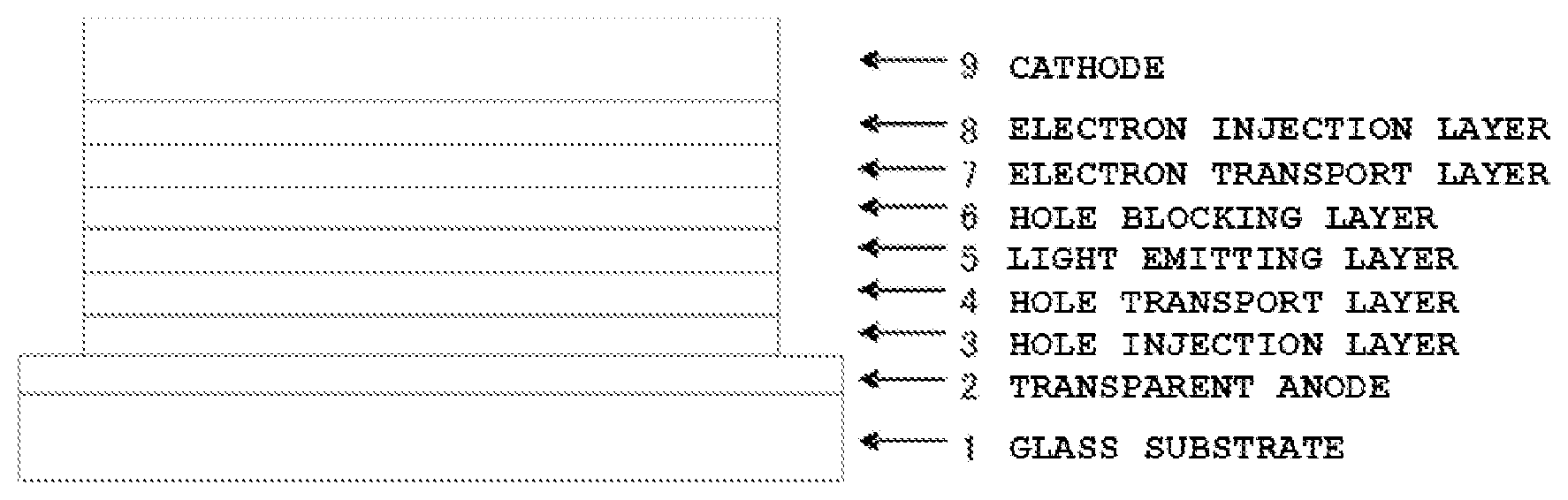
The FIGURE is a diagram illustrating the configuration of the organic EL devices of Examples 29 to 43 and Comparative Examples 1 to 2.
DESCRIPTION OF EMBODIMENTS
These compounds can be synthesized, for example, according to a known method as described below (refer to PTLs 5 and 6, NPLs 6 and 7, for example).
The following presents specific examples of preferred compounds among the benzoxazole compounds of the general formula (1) preferably used in the organic EL device of the present invention. The present invention, however, is not restricted to these compounds.
The following presents specific examples of preferred compounds among the benzothiazole compounds of the general formula (1) preferably used in the organic EL device of the present invention. The present invention, however, is not restricted to these compounds.
The compounds described above having an fused-azole ring structure can be synthesized by a known method (refer to PTLs 5 and 6, NPLs 6 and 7, for example).
The compounds having a fused-azole ring structure of the general formula (1) were purified by methods such as column chromatography, adsorption using, for example, a silica gel, activated carbon, or activated clay, recrystallization or crystallization using a solvent, and a sublimation purification method. The compounds were identified by an NMR analysis. A melting point, a glass transition point (Tg), and a work function were measured as material property values. The melting point can be used as an index of vapor deposition, the glass transition point (Tg) can be used as an index of stability in a thin-film state, and the work function can be used as an index of hole transportability and hole blocking performance.
Other compounds used for the organic EL device of the present invention were purified by methods such as column chromatography, adsorption using, for example, a silica gel, activated carbon, or activated clay, recrystallization or crystallization using a solvent, and a sublimation purification method, and finally purified by a sublimation purification method.
The melting point and the glass transition point (Tg) were measured by a high-sensitive differential scanning calorimeter (DSC3100SA produced by Bruker AXS) using powder.
For the measurement of the work function, a 100 nm-thick thin film was fabricated on an ITO substrate, and an ionization potential measuring device (PYS-202 produced by Sumitomo Heavy Industries, Ltd.) was used.
The organic EL device of the present invention may have a structure including an anode, a hole injection layer, a hole transport layer, a light emitting layer, an electron transport layer, an electron injection layer, and a cathode successively formed on a substrate, optionally with an electron blocking layer between the hole transport layer and the light emitting layer, and a hole blocking layer between the light emitting layer and the electron transport layer. Some of the organic layers in the multilayer structure may be omitted, or may serve more than one function. For example, a single organic layer may serve as the hole injection layer and the hole transport layer, or as the electron injection layer and the electron transport layer, and so on. Further, any of the layers may be configured to laminate two or more organic layers having the same function, and the hole transport layer may have a two-layer laminated structure, the light emitting layer may have a two-layer laminated structure, the electron transport layer may have a two-layer laminated structure, and so on.
An electrode material having a high work function, such as ITO and gold, may be used as the anode of the organic EL device of the present invention. The hole injection layer used of the organic EL device of the present invention may be a porphyrin compound, represented by copper phthalocyanine, and also may be a starburst type triphenylamine derivative, a triphenylamine trimer or tetramer, such as an arylamine compound having a structure containing in the molecule thereof three or more triphenylamine structures binding via a single bond or a divalent group containing no hetero atom, a heterocyclic compound having acceptor property, such as hexacyanoazatriphenylene, or a coating type polymer compound. These materials may be formed into a thin film by a vapor deposition method or other known methods such as a spin coating method and an inkjet method.
Examples of material used for the hole transport layer of the organic EL device of the present invention can be benzidine derivatives such as N,N′-diphenyl-N,N′-di(m-tolyl)-benzidine (hereinafter referred to as TPD), N,N′-diphenyl-N,N′-di(a-naphthyl)-benzidine (hereinafter referred to as NPD), and N,N,N′,N′-tetrabiphenylylbenzidine; 1,1-bis[(di-4-tolylamino)phenyl]cyclohexane (TAPC); various triphenylamine trimers and tetramers. These may be individually deposited for film forming, may be used as a single layer deposited mixed with other materials, or may be formed as a laminate of individually deposited layers, a laminate of mixedly deposited layers, or a laminate of the individually deposited layer and the mixedly deposited layer. Examples of material used for the hole injection/transport layer can be coating-type polymer materials such as poly(3,4-ethylenedioxythiophene) (PEDOT)/poly(styrene sulfonate) (PSS). These materials may be formed into a thin-film by a vapor deposition method or other known methods such as a spin coating method and an inkjet method.
In the hole injection layer or the hole transport layer, a material that is ordinarily used in the layer p-doped with trisbromophenylamine hexachloro antimony, or the like, a polymer compound having a structure of a benzidine derivative, such as TPD, as a partial structure thereof, or the like may be used.
The electron blocking layer used of the organic EL device of the present invention may be a compound having an electron blocking capability, such as a carbazole derivative, such as 4,4′,4″-tri(N-carbazolyl)triphenylamine (hereinafter referred to as TCTA), 9,9-bis[4-(carbazol-9-yl)phenyl]fluorene, 1,3-bis(carbazol-9-yl)benzene (hereinafter referred to as mCP), and 2,2-bis(4-carbazol-9-ylphenyl)adamantane (Ad-Cz), a compound having a triphenylsilyl group and a triarylamine structure, represented by 9-[4-(carbazol-9-yl)phenyl]-9-[4-(triphenylsilyl)phenyl]-9H-fluorene. These compounds each may be individually formed into a film, may be used as a single layer formed with another material mixed, or may be formed into a laminated structure containing the individually formed layers, a laminated structure containing the layers with another material mixed, or a laminated structure containing the individually formed layer and the layer with another material mixed. These materials may be formed into a thin film by a vapor deposition method or other known methods such as a spin coating method and an inkjet method.
Examples of material used for the light emitting layer of the organic EL device of the present invention can be various metal complexes including, for example, quinolinol derivative metal complexes such as Alq 3 ; anthracene derivatives; bis(styryl)benzene derivatives; pyrene derivatives; oxazole derivatives; and polyparaphenylene vinylene derivatives; in addition to the compounds having a fused-azole ring structure of the present invention. Further, the light emitting layer may be made of a host material and a dopant material. Examples of the host material can be the above light-emitting materials, thiazole derivatives, benzimidazole derivatives, and polydialkyl fluorene derivatives, in addition to the compounds having a fused-azole ring structure of the present invention and the compounds having a pyridoindole ring structure. Examples of the dopant material can be quinacridone, coumarin, rubrene, perylene, derivatives thereof, benzopyran derivatives, rhodamine derivatives, and aminostyryl derivatives. These may be individually deposited for film forming, may be used as a single layer deposited mixed with other materials, or may be formed as a laminate of individually deposited layers, a laminate of mixedly deposited layers, or a laminate of the individually deposited layer and the mixedly deposited layer.
Further, the light-emitting material may be a phosphorescent material. Phosphorescent materials as metal complexes such as iridium and platinum may be used. Examples of the phosphorescent materials include green phosphorescent materials such as Ir(ppy)3, blue phosphorescent materials such as FIrpic and FIr6, and red phosphorescent materials such as Btp 2 Ir(acac). Here, carbazole derivatives such as 4,4′-di(N-carbazolyl)biphenyl (CBP), TCTA, and mCP may be used as the hole injecting and transporting host material, in addition to the compounds having a fused-azole ring structure of the present invention and the compounds having a pyridoindole ring structure. Compounds such as p-bis(triphenylsilyl)benzene (UGH2) and 2,2′,2″-(1,3,5-phenylene)-tris(1-phenyl-1H-benzimidazole) (TPBI) may be used as the electron transporting host material. In this way, a high-performance organic EL device can be produced.
In order to avoid concentration quenching, the doping of the host material with the phosphorescent light emitting material is preferably made by co-evaporation in a range of 1 to 30% by weight with respect to the total light emitting layer.
Further, Examples of the light emitting material may be delayed fluorescent-emitting material such as a CDCB derivative of PIC-TRZ, CC2TA, PXZ-TRZ, 4CzIPN or the like (refer to NPL 3, for example).
These materials may be formed into a thin film by using a vapor deposition method or other known methods such as a spin coating method and an inkjet method.
The hole blocking layer of the organic EL device of the present invention may be formed by using hole blocking compounds such as the metal complexes of phenanthroline derivatives such as bathocuproin (hereinafter referred to as BCP), the metal complexes of quinolinol derivatives such as BAlq, various rare earth complexes, oxazole derivatives, triazole derivatives, and triazine derivatives, in addition to the compounds having a fused-azole ring structure of the present invention. These materials may also serve as the material of the electron transport layer. These may be individually deposited for film forming, may be used as a single layer deposited mixed with other materials, or may be formed as a laminate of individually deposited layers, a laminate of mixedly deposited layers, or a laminate of the individually deposited layer and the mixedly deposited layer. These materials may be formed into a thin-film by using a vapor deposition method or other known methods such as a spin coating method and an inkjet method.
The electron transport layer of the organic EL device of the present invention may be formed by using metal complexes of quinolinol derivatives such as Alq 3 and BAlq, various metal complexes, triazole derivatives, triazine derivatives, oxadiazole derivatives, pyridine derivatives, benzimidazole derivatives, thiadiazole derivatives, anthracene derivatives, carbodiimide derivatives, quinoxaline derivatives, Pyridoindole derivatives, phenanthroline derivatives, and silole derivatives, in addition to the compounds of having a fused-azole ring structure of the present invention. These may be individually deposited for film forming, may be used as a single layer deposited mixed with other materials, or may be formed as a laminate of individually deposited layers, a laminate of mixedly deposited layers, or a laminate of the individually deposited layer and the mixedly deposited layer. These materials may be formed into a thin-film by using a vapor deposition method or other known methods such as a spin coating method and an inkjet method.
Examples of material used for the electron injection layer of the organic EL device of the present invention can be alkali metal salts such as lithium fluoride and cesium fluoride; alkaline earth metal salts such as magnesium fluoride; a metal complex of a quinolinol derivative such as lithium quinolinol; and metal oxides such as aluminum oxide; in addition to the compounds having a fused-azole ring structure of the present invention. However, the electron injection layer may be omitted in the preferred selection of the electron transport layer and the cathode.
Further, in the electron injection layer or the electron transport layer, a material obtained by further N-doping a material which is commonly used for the layer with a metal such as cecium, or the like can be used.
The cathode of the organic EL device of the present invention may be made of an electrode material with a low work function such as aluminum, or an alloy of an electrode material with an even lower work function such as a magnesium-silver alloy, a magnesium-indium alloy, or an aluminum-magnesium alloy.
The following describes an embodiment of the present invention in more detail based on Examples. The present invention, however, is not restricted to the following Examples, as long as such departures are within the scope of the invention.
Example 1
Synthesis of 4,6-bis(4-naphthalene-1-yl-phenyl)-2-(4-pyridine-3-yl-phenyl)-benzoxazole (Compound 1-1)
2-(4-chlorophenyl)-4,6-bis(4-naphthalene-1-yl-phenyl)-benzoxazole (4.5 g), 3-pyridylboronic acid (1.0 g), bis(dibenzylideneacetone)palladium(0) (0.32 g), tricyclohexylphosphine (0.4 g), and tripotassium phosphate (4.7 g) were added into reaction vessel. The mixture was refluxed for overnight while stirring. After cooling, an organic layer was collected by liquid separation, and ethyl acetate were added to the aqueous layer for extraction. The collected organic layer was concentrated, and then the resulting crude product was purified by column chromatography (support: silica gel, eluent: dichloromethane/ethyl acetate), and the crystallization with a dichloromethane/methanol mixed solvent whereby a white powder of 4,6-bis(4-naphthalene-1-yl-phenyl)-2-(4-pyridine-3-yl-phenyl)-benzoxazole (Compound 1-1; 1.8 g; yield: 38%) was obtained.
The structure of the obtained white powder was identified by NMR.
1 H-NMR (CDCl 3 ) detected 32 hydrogen signals, as follows.
δ(ppm)=8.98 (1H), 8.68 (1H), 8.52 (2H), 8.34 (2H), 8.12 (1H), 8.07-7.89 (10H), 7.82 (2H), 7.76 (2H), 7.69 (2H), 7.64 (9H).
Example 2
Synthesis of 2-{4′-(pyridine-3-yl)-1,1′-biphenyl-4-yl}-4,6-di(naphthalene-1-yl)-benzoxazole (Compound 1-2)
The reaction was carried out under the same conditions as those of Example 1, except that 2-(4-chlorophenyl)-4,6-bis(4-naphthalene-1-yl-phenyl)-benzoxazole was replaced with 2-(4-chlorophenyl)-4,6-di(naphthalene-1-yl)-benzoxazole, and 3-pyridylboronic acid was replaced with 4-(pyridine-3-yl)-phenylboronic acid, whereby a white powder of 2-{4′-(pyridine-3-yl)-1,1′-biphenyl-4-yl}-4,6-di(naphthalene-1-yl)-benzoxazole (Compound 1-2; 2.1 g; yield: 34%) was obtained.
The structure of the obtained white powder was identified by NMR.
1 H-NMR (CDCl 3 ) detected 28 hydrogen signals, as follows.
δ(ppm)=8.94 (1H), 8.64 (1H), 8.35 (2H), 8.13 (1H), 8.05-7.91 (6H), 7.85 (1H), 7.82-7.76 (5H), 7.72 (2H), 7.68 (2H), 7.64-7.38 (7H).
Example 3
Synthesis of 4,6-bis(4-naphthalene-1-yl-phenyl)-2-(3-pyridine-3-yl-phenyl)-benzoxazole (Compound 1-3)
The reaction was carried out under the same conditions as those of Example 1, except that 2-(4-chlorophenyl)-4,6-bis(4-naphthalene-1-yl-phenyl)-benzoxazole was replaced with 2-(3-chlorophenyl)-4,6-bis(4-naphthalene-1-yl-phenyl)-benzoxazole, and bis(dibenzylideneacetone)palladium(0) was replaced with tris(dibenzylideneacetone)palladium(0), whereby a white powder of 4,6-bis(4-naphthalene-1-yl-phenyl)-2-(3-pyridine-3-yl-phenyl)-benzoxazole (Compound 1-3; 3.6 g; yield: 48%) was obtained.
The structure of the obtained white powder was identified by NMR.
1 H-NMR (CDCl 3 ) detected 32 hydrogen signals, as follows.
δ(ppm)=9.01 (1H), 8.69 (1H), 8.60 (1H), 8.43 (1H), 8.32 (2H), 8.11 (1H), 8.07-8.01 (3H), 7.98-7.88 (7H), 7.83-7.67 (6H), 7.62-7.42 (9H).
Example 4
Synthesis of 2-{3′-(pyridine-3-yl)-1,1′-biphenyl-4-yl}-4,6-di(naphthalene-1-yl)-benzoxazole (Compound 1-4)
The reaction was carried out under the same conditions as those of Example 1, except that 2-(4-chlorophenyl)-4,6-bis(4-naphthalene-1-yl-phenyl)-benzoxazole was replaced with 2-(4-chlorophenyl)-4,6-di(naphthalene-1-yl)-benzoxazole, and 3-pyridylboronic acid was replaced with 3-(pyridine-3-yl)-phenylboronic acid, and bis(dibenzylideneacetone)palladium(0) was replaced with tris(dibenzylideneacetone)palladium(0), whereby a white powder of 2-{3′-(pyridine-3-yl)-1,1′-biphenyl-4-yl}-4,6-di(naphthalene-1-yl)-benzoxazole (Compound 1-4; 4.4 g; yield: 71%) was obtained.
The structure of the obtained white powder was identified by NMR.
1 H-NMR (CDCl 3 ) detected 28 hydrogen signals, as follows.
δ(ppm)=8.94 (1H), 8.65 (1H), 8.36 (2H), 8.21 (1H), 8.05-7.92 (6H), 7.85 (2H), 7.83-7.76 (3H), 7.75-7.74 (12H).
Example 5
Synthesis of 2-(3-pyridine-4-yl-phenyl)-4,6-bis(4-naphthalene-1-yl-phenyl)-benzoxazole (Compound 1-5)
The reaction was carried out under the same conditions as those of Example 1, except that 2-(4-chlorophenyl)-4,6-bis(4-naphthalene-1-yl-phenyl)-benzoxazole was replaced with 2-(3-chlorophenyl)-4,6-bis(4-naphthalene-1-yl-phenyl)-benzoxazole, and 3-pyridylboronic acid was replaced with 4-pyridylboronic acid, and bis(dibenzylideneacetone)palladium(0) was replaced with tris(dibenzylideneacetone)palladium(0), whereby a white powder of 2-(3-pyridine-4-yl-phenyl)-4,6-bis(4-naphthalene-1-yl-phenyl)-benzoxazole (Compound 1-5; 3.0 g; yield: 40%) was obtained.
The structure of the obtained white powder was identified by NMR.
1 H-NMR (CDCl 3 ) detected 32 hydrogen signals, as follows.
δ(ppm)=8.76 (2H), 8.66 (1H), 8.47 (1H), 8.32 (2H), 8.11 (1H), 8.07-8.02 (2H), 7.99-7.89 (7H), 7.85 (1H), 7.78-7.48 (15H).
Example 6
Synthesis of 2-{4′-(pyridine-3-yl)-1,1′-biphenyl-4-yl}-4,6-di(phenanthrene-9-yl)-benzoxazole (Compound 1-6)
The reaction was carried out under the same conditions as those of Example 1, except that 2-(4-chlorophenyl)-4,6-bis(4-naphthalene-1-yl-phenyl)-benzoxazole was replaced with 2-(4-chlorophenyl)-4,6-di(phenanthrene-9-yl)-benzoxazole, and 3-pyridylboronic acid was replaced with 4-(pyridine-3-yl)phenylboronic acid, and bis(dibenzylideneacetone)palladium(0) was replaced with tris(dibenzylideneacetone)palladium(0), whereby a white powder of 2-{4′-(pyridine-3-yl)-1,1′-biphenyl-4-yl}-4,6-di(phenanthrene-9-yl)-benzoxazole (Compound 1-6; 2.1 g; yield: 17%) was obtained.
The structure of the obtained white powder was identified by NMR.
1 H-NMR (CDCl 3 ) detected 32 hydrogen signals, as follows.
δ(ppm)=8.93 (1H), 8.87-8.63 (4H), 8.62 (1H), 8.33 (2H), 8.18 (1H), 8.08-7.88 (7H), 7.80-7.55 (15H), 7.40 (1H).
Example 7
Synthesis of 2-{3′-(pyridine-3-yl)-1,1′-biphenyl-3-yl}-4,6-bis(4-naphthalene-1-yl-phenyl)-benzoxazole (Compound 1-7)
The reaction was carried out under the same conditions as those of Example 1, except that 2-(4-chlorophenyl)-4,6-bis(4-naphthalene-1-yl-phenyl)-benzoxazole was replaced with 2-(3-chlorophenyl)-4,6-bis(4-naphthalene-1-yl-phenyl)-benzoxazole, and 3-pyridylboronic acid was replaced with 3-(pyridine-3-yl)phenylboronic acid, and bis(dibenzylideneacetone)palladium(0) was replaced with tris(dibenzylideneacetone)palladium(0), whereby a white powder of 2-{3′-(pyridine-3-yl)-1,1′-biphenyl-3-yl}-4,6-bis(4-naphthalene-1-yl-phenyl)-benzoxazole (Compound 1-7; 2.0 g; yield: 27%) was obtained.
The structure of the obtained white powder was identified by NMR.
1 H-NMR (CDCl 3 ) detected 36 hydrogen signals, as follows.
δ(ppm)=8.98 (1H), 8.68-8.61 (2H), 8.42 (1H), 8.32 (2H), 8.15-7.40 (30H).
Example 8
Synthesis of 2-{3′-(pyridine-3-yl)-1,1′-biphenyl-4-yl}-4,6-di(phenanthrene-9-yl)-benzoxazole (Compound 1-8)
The reaction was carried out under the same conditions as those of Example 1, except that 2-(4-chlorophenyl)-4,6-bis(4-naphthalene-1-yl-phenyl)-benzoxazole was replaced with 2-(4-chlorophenyl)-4,6-di(phenanthrene-9-yl)-benzoxazole, and 3-pyridylboronic acid was replaced with 3-(pyridine-3-yl)phenylboronic acid, and bis(dibenzylideneacetone)palladium(0) was replaced with tris(dibenzylideneacetone)palladium(0), whereby a white powder of 2-{3′-(pyridine-3-yl)-1,1′-biphenyl-4-yl}-4,6-di(phenanthrene-9-yl)-benzoxazole (Compound 1-8; 4.0 g; yield: 33%) was obtained.
The structure of the obtained white powder was identified by NMR.
1 H-NMR (CDCl 3 ) detected 32 hydrogen signals, as follows.
δ(ppm)=8.93 (1H), 8.87-8.73 (4H), 8.65 (1H), 8.36 (2H), 8.18 (1H), 8.08-7.83 (8H), 7.79-7.54 (14H), 7.42 (1H).
Example 9
Synthesis of 6-(biphenyl-3-yl)-2-(biphenyl-4-yl)-4-(9-phenyl-[9H]-carbazol-3-yl)-benzoxazole (Compound 1-73)
The reaction was carried out under the same conditions as those of Example 1, except that 2-(4-chlorophenyl)-4,6-bis(4-naphthalene-1-yl-phenyl)-benzoxazole was replaced with 6-(biphenyl-3-yl)-2-(4-chlorophenyl)-4-(9-phenyl-[9H]-carbazol-3-yl)-benzoxazole, and 3-pyridylboronic acid was replaced with phenylboronic acid, whereby a white powder of 6-(biphenyl-3-yl)-2-(biphenyl-4-yl)-4-(9-phenyl-[9H]-carbazol-3-yl)-benzoxazole (Compound 1-73; 3.0 g; yield: 44%) was obtained.
The structure of the obtained white powder was identified by NMR.
1 H-NMR (CDCl 3 ) detected 32 hydrogen signals, as follows.
δ(ppm)=8.90 (1H), 8.45 (2H), 8.30 (1H), 8.26 (1H), 7.94 (1H), 7.91 (1H), 7.85 (2H), 7.80 (3H), 7.74-7.32 (20H).
Example 10
Synthesis of 2-{3′-(pyridine-3-yl)-biphenyl-4-yl}-6-(9,9′-spirobi[9H]fluorene-2-yl)-benzoxazole (Compound 1-91)
The reaction was carried out under the same conditions as those of Example 1, except that 2-(4-chlorophenyl)-4,6-bis(4-naphthalene-1-yl-phenyl)-benzoxazole was replaced with 2-(4-chlorophenyl)-6-(9,9′-spirobi[9H]fluorene-2-yl)-benzoxazole, and 3-pyridylboronic acid was replaced with 3-(pyridine-3-yl)-phenylboronic acid, and bis(dibenzylideneacetone)palladium(0) was replaced with tris(dibenzylideneacetone)palladium(0), whereby a white powder of 2-{3′-(pyridine-3-yl)-biphenyl-4-yl}-6-(9,9′-spirobi[9H]fluorene-2-yl)-benzoxazole (Compound 1-91; 10.5 g; yield: 58%) was obtained.
The structure of the obtained white powder was identified by NMR.
1 H-NMR (CDCl 3 ) detected 30 hydrogen signals, as follows.
δ(ppm)=8.94 (1H), 8.66 (1H), 8.33 (2H), 8.01-7.77 (8H), 7.77-7.57 (6H), 7.52-7.37 (5H), 7.15 (3H), 7.03 (1H), 6.82 (2H), 6.78 (1H).
Example 11
Synthesis of 4,6-bis(biphenyl-3-yl)-2-([1,1′:3′,1″]terphenyl-4-yl)-benzoxazole (Compound 1-96)
The reaction was carried out under the same conditions as those of Example 1, except that 2-(4-chlorophenyl)-4,6-bis(4-naphthalene-1-yl-phenyl)-benzoxazole was replaced with 4,6-bis(biphenyl-3-yl)-2-(4-chlorophenyl)-benzoxazole, and 3-pyridylboronic acid was replaced with 3-biphenylboronic acid, whereby a white powder of 4,6-bis(biphenyl-3-yl)-2-([1,1′:3′,1″]terphenyl-4-yl)-benzoxazole (Compound 1-96; 8.3 g; yield: 68.0%) was obtained.
The structure of the obtained white powder was identified by NMR.
1 H-NMR (CDCl 3 ) detected 33 hydrogen signals, as follows.
δ(ppm)=8.44 (2H), 8.35 (1H), 8.14 (1H), 8.00-7.82 (6H), 7.80-7.47 (20H), 7.46-7.37 (3H).
Example 12
Synthesis of 4,6-di(dibenzofuran-4-yl)-2-(4-pyridine-3-yl-phenyl)-benzoxazole (Compound 1-100)
The reaction was carried out under the same conditions as those of Example 1, except that 2-(4-chlorophenyl)-4,6-bis(4-naphthalene-1-yl-phenyl)-benzoxazole was replaced with 2-(4-chlorophenyl)-4,6-di(dibenzofuran-4-yl)-benzoxazole, and bis(dibenzylideneacetone)palladium(0) was replaced with tris(dibenzylideneacetone)palladium(0), whereby a yellow powder of 4,6-di(dibenzofuran-4-yl)-2-(4-pyridine-3-yl-phenyl)-benzoxazole (Compound 1-100; 7.3 g; yield: 61%) was obtained.
The structure of the obtained yellow powder was identified by NMR.
1 H-NMR (CDCl 3 ) detected 24 hydrogen signals, as follows.
δ(ppm)=8.96 (1H), 8.67 (1H), 8.59 (1H), 8.47 (2H), 8.37 (1H), 8.32 (1H), 8.06 (4H), 7.99 (1H), 7.84 (1H), 7.78 (2H), 7.69 (1H), 7.62 (1H), 7.61 (1H), 7.58-7.36 (6H).
Example 13
Synthesis of 2,6-diphenyl-4-(9,9′-spirobi[9H]fluorene-2-yl)-benzoxazole (Compound 1-106)
The reaction was carried out under the same conditions as those of Example 1, except that 2-(4-chlorophenyl)-4,6-bis(4-naphthalene-1-yl-phenyl)-benzoxazole was replaced with 6-chloro-2-phenyl-4-(9,9′-spirobi[9H]fluorene-2-yl)-benzoxazole, and 3-pyridylboronic acid was replaced with phenylboronic acid, whereby a white powder of 2,6-diphenyl-4-(9,9′-spirobi[9H]fluorene-2-yl)-benzoxazole (Compound 1-106; 4.5 g; yield: 41%) was obtained.
The structure of the obtained white powder was identified by NMR.
1 H-NMR (CDCl 3 ) detected 27 hydrogen signals, as follows.
δ(ppm)=8.15-7.98 (6H), 7.97-7.85 (4H), 7.60-7.36 (9H), 7.17 (4H), 6.90-6.80 (4H).
Example 14
Synthesis of 2-{3,5-di([9H]-carbazol-9-yl)-phenyl}-4,6-diphenyl-benzoxazole (Compound 1-107)
The reaction was carried out under the same conditions as those of Example 1, except that 2-(4-chlorophenyl)-4,6-bis(4-naphthalene-1-yl-phenyl)-benzoxazole was replaced with 2-(3,5-dichlorophenyl)-4,6-diphenyl-benzoxazole, and 3-pyridylboronic acid was replaced with carbazol, whereby a white powder of 2-{3,5-di([9H]-carbazol-9-yl)-phenyl}-4,6-diphenyl-benzoxazole (Compound 1-107; 4.8 g; yield: 30%) was obtained.
The structure of the obtained white powder was identified by NMR.
1 H-NMR (CDCl 3 ) detected 31 hydrogen signals, as follows.
δ(ppm)=8.67 (2H), 8.21 (4H), 8.10 (2H), 8.01 (1H), 7.85 (1H), 7.79 (1H), 7.73 (2H), 7.63 (4H), 7.57-7.46 (8H), 7.46-7.33 (6H).
Example 15
Synthesis of 4-(4-naphthalene-1-yl-phenyl)-6-{9-phenyl-[9H]-carbazol-3-yl)-2-(3-pyridine-3-yl-phenyl)-benzoxazole (Compound 1-108)
The reaction was carried out under the same conditions as those of Example 1, except that 2-(4-chlorophenyl)-4,6-bis(4-naphthalene-1-yl-phenyl)-benzoxazole was replaced with 2-(3-chlorophenyl)-4-(4-naphthalene-1-yl-phenyl)-6-(9-phenyl-[9H]-carbazol-3-yl)-benzoxazole, whereby a white powder of 4-(4-naphthalene-1-yl-phenyl)-6-(9-phenyl-[9H]-carbazol-3-yl)-2-(3-pyridine-3-yl-phenyl)-benzoxazole (Compound 1-108; 2.6 g; yield: 47%) was obtained.
The structure of the obtained white powder was identified by NMR.
1 H-NMR (CDCl 3 ) detected 33 hydrogen signals, as follows.
δ(ppm)=9.01 (1H), 8.69 (1H), 8.61 (1H), 8.53 (1H), 8.44 (1H), 8.35 (2H), 8.28 (1H), 8.14 (1H), 8.06 (1H), 8.05 (1H), 7.97 (1H), 7.96 (1H), 7.93 (1H), 7.86-7.42 (18H), 7.37 (1H).
Example 16
Synthesis of 2-phenyl-6-(9-phenyl-[9H]-carbazol-3-yl)-4-(5-phenyl-[5H]-pyrido[4,3-b]indole-8-yl)-benzoxazole (Compound 1-110)
The reaction was carried out under the same conditions as those of Example 1, except that 2-(4-chlorophenyl)-4,6-bis(4-naphthalene-1-yl-phenyl)-benzoxazole was replaced with 6-chloro-2-phenyl-4-(5-phenyl-[5H]-pyrido[4,3-b]indole-8-yl)-benzoxazole, and 3-pyridylboronic acid was replaced with 9-phenyl-[9H]-carbazol-3-yl-boronic acid, whereby a yellow powder of 2-phenyl-6-(9-phenyl-[9H]-carbazol-3-yl)-4-(5-phenyl-[5H]-pyrido[4,3-b]indole-8-yl)-benzoxazole (Compound 1-110; 2.9 g; yield: 50%) was obtained.
The structure of the obtained yellow powder was identified by NMR.
1 H-NMR (CDCl 3 ) detected 30 hydrogen signals, as follows.
δ(ppm)=9.56 (1H), 9.04 (1H), 8.59 (1H), 8.53 (1H), 8.48 (1H), 8.45 (1H), 8.36 (1H), 8.26 (2H), 8.05 (1H), 7.93 (2H), 7.88-7.43 (16H), 7.36 (2H).
Example 17
Synthesis of 6-(4-naphthalene-1-yl-phenyl)-2-(biphenyl-4-yl)-4-(4-pyridine-3-yl-phenyl)-benzoxazole (Compound 1-112)
The reaction was carried out under the same conditions as those of Example 1, except that 2-(4-chlorophenyl)-4,6-bis(4-naphthalene-1-yl-phenyl)-benzoxazole was replaced with 2-(4-chlorophenyl)-6-(4-naphthalene-1-yl-phenyl)-4-(4-pyridine-3-yl-phenyl)-benzoxazole, and 3-pyridylboronic acid was replaced with phenylboronic acid, and bis(dibenzylideneacetone)palladium(0) was replaced with tris(dibenzylideneacetone)palladium(0), whereby a white powder of 6-(4-naphthalene-1-yl-phenyl)-2-(biphenyl-4-yl)-4-(4-pyridine-3-yl-phenyl)-benzoxazole (Compound 1-112; 4.8 g; yield: 56%) was obtained.
The structure of the obtained white powder was identified by NMR.
1 H-NMR (CDCl 3 ) detected 30 hydrogen signals, as follows.
δ(ppm)=9.00 (1H), 8.66 (1H), 8.45 (2H), 8.33 (2H), 8.07-7.78 (12H), 7.70 (4H), 7.63-7.40 (8H).
Example 18
Synthesis of 2,6-bis(4-naphthalene-1-yl-phenyl)-4-(4-pyridine-3-yl-phenyl)-benzoxazole (Compound 1-113)
The reaction was carried out under the same conditions as those of Example 1, except that 2-(4-chlorophenyl)-4,6-bis(4-naphthalene-1-yl-phenyl)-benzoxazole was replaced with 2-(4-chlorophenyl)-6-(4-naphthalene-1-yl-phenyl)-4-(4-pyridine-3-yl-phenyl)-benzoxazole, and 3-pyridylboronic acid was replaced with 1-naphthaleneboronic acid, and bis(dibenzylideneacetone)palladium(0) was replaced with tris(dibenzylideneacetone)palladium(0), whereby a white powder of 2,6-bis(4-naphthalene-1-yl-phenyl)-4-(4-pyridine-3-yl-phenyl)-benzoxazole (Compound 1-113; 6.1 g; yield: 66%) was obtained.
The structure of the obtained white powder was identified by NMR.
1 H-NMR (CDCl 3 ) detected 32 hydrogen signals, as follows.
δ(ppm)=9.01 (1H), 8.66 (1H), 8.51 (2H), 8.35 (2H), 8.09-7.80 (13H), 7.73 (2H), 7.69 (2H), 7.64-7.40 (9H).
Example 19
Synthesis of 2-(biphenyl-4-yl)-6-(phenanthrene-9-yl)-4-(4-pyridine-3-yl-phenyl)-benzoxazole (Compound 1-118)
The reaction was carried out under the same conditions as those of Example 1, except that 2-(4-chlorophenyl)-4,6-bis(4-naphthalene-1-yl-phenyl)-benzoxazole was replaced with 2-(4-chlorophenyl)-6-(phenanthrene-9-yl)-4-(4-pyridine-3-yl-phenyl)-benzoxazole, and 3-pyridylboronic acid was replaced with phenylboronic acid, and bis(dibenzylideneacetone)palladium(0) was replaced with tris(dibenzylideneacetone)palladium(0), whereby a white powder of 2-(biphenyl-4-yl)-6-(phenanthrene-9-yl)-4-(4-pyridine-3-yl-phenyl)-benzoxazole (Compound 1-118; 4.3 g; yield: 67%) was obtained.
The structure of the obtained white powder was identified by NMR.
1 H-NMR (CDCl 3 ) detected 28 hydrogen signals, as follows.
δ(ppm)=8.98 (1H), 8.86 (1H), 8.80 (1H), 8.64 (1H), 8.46 (2H), 8.32 (2H), 8.07 (1H), 7.98 (2H), 7.88-7.57 (13H), 7.52 (2H), 7.44 (2H).
Example 20
Synthesis of 2-(biphenyl-4-yl)-6-(phenanthrene-9-yl)-4-(3-pyridine-3-yl-phenyl)-benzoxazole (Compound 1-119)
The reaction was carried out under the same conditions as those of Example 1, except that 2-(4-chlorophenyl)-4,6-bis(4-naphthalene-1-yl-phenyl)-benzoxazole was replaced with 2-(4-chlorophenyl)-6-(phenanthrene-9-yl)-4-(3-pyridine-3-yl-phenyl)-benzoxazole, and 3-pyridylboronic acid was replaced with phenylboronic acid, and bis(dibenzylideneacetone)palladium(0) was replaced with tris(dibenzylideneacetone)palladium(0), whereby a white powder of 2-(biphenyl-4-yl)-6-(phenanthrene-9-yl)-4-(3-pyridine-3-yl-phenyl)-benzoxazole (Compound 1-119; 3.0 g; yield: 35%) was obtained.
The structure of the obtained white powder was identified by NMR.
1 H-NMR (CDCl 3 ) detected 28 hydrogen signals, as follows.
δ(ppm)=9.02 (1H), 8.85 (1H), 8.79 (1H), 8.64 (1H), 8.45 (2H), 8.43 (1H), 8.19 (1H), 8.07 (1H), 8.02 (1H), 7.97 (1H), 7.89-7.78 (5H), 7.78-7.39 (12H).
Example 21
Synthesis of 6-(phenanthrene-9-yl)-4-(4-pyridine-3-yl-phenyl)-2-([1,1′:4′,1″]terphenyl-4-yl)-benzoxazole (Compound 1-120)
The reaction was carried out under the same conditions as those of Example 1, except that 2-(4-chlorophenyl)-4,6-bis(4-naphthalene-1-yl-phenyl)-benzoxazole was replaced with 2-(4-chlorophenyl)-6-(phenanthrene-9-yl)-4-(4-pyridine-3-yl-phenyl)-benzoxazole, and 3-pyridylboronic acid was replaced with 4-biphenylboronic acid, and bis(dibenzylideneacetone)palladium(0) was replaced with tris(dibenzylideneacetone)palladium(0), whereby a white powder of 6-(phenanthrene-9-yl)-4-(4-pyridine-3-yl-phenyl)-2-([1,1′:4′,1″]terphenyl-4-yl)-benzoxazole (Compound 1-120; 2.8 g; yield: 36%) was obtained.
The structure of the obtained white powder was identified by NMR.
1 H-NMR (CDCl 3 ) detected 32 hydrogen signals, as follows.
δ(ppm)=8.98 (1H), 8.86 (1H), 8.80 (1H), 8.64 (1H), 8.48 (2H), 8.33 (2H), 8.08 (1H), 7.98 (2H), 7.90-7.57 (17H), 7.51 (2H), 7.41 (2H).
Example 22
Synthesis of 2-(4-naphthalene-2-yl-phenyl)-6-(phenanthrene-9-yl)-4-(4-pyridine-3-yl-phenyl)-benzoxazole (Compound 1-122)
The reaction was carried out under the same conditions as those of Example 1, except that 2-(4-chlorophenyl)-4,6-bis(4-naphthalene-1-yl-phenyl)-benzoxazole was replaced with 2-(4-chlorophenyl)-6-(phenanthrene-9-yl)-4-(4-pyridine-3-yl-phenyl)-benzoxazole, and 3-pyridylboronic acid was replaced with 2-naphthaleneboronic acid, and bis(dibenzylideneacetone)palladium(0) was replaced with tris(dibenzylideneacetone)palladium(0), whereby a white powder of 2-(4-naphthalene-2-yl-phenyl)-6-(phenanthrene-9-yl)-4-(4-pyridine-3-yl-phenyl)-benzoxazole (Compound 1-122; 3.0 g; yield: 43%) was obtained.
The structure of the obtained white powder was identified by NMR.
1 H-NMR (CDCl 3 ) detected 30 hydrogen signals, as follows.
δ(ppm)=8.98 (1H), 8.86 (1H), 8.80 (1H), 8.65 (1H), 8.51 (2H), 8.33 (2H), 8.17 (1H), 8.08 (1H), 8.03-7.90 (7H), 7.89-7.51 (12H), 7.42 (1H).
Example 23
Synthesis of 2-phenyl-4-(4-pyridine-3-yl-phenyl)-6-(triphenylene-2-yl)-benzoxazole (Compound 1-125)
The reaction was carried out under the same conditions as those of Example 1, except that 2-(4-chlorophenyl)-4,6-bis(4-naphthalene-1-yl-phenyl)-benzoxazole was replaced with 6-chloro-2-phenyl-4-(4-pyridine-3-yl-phenyl)-benzoxazole, and 3-pyridylboronic acid was replaced with 2-triphenyleneboronic acid, and bis(dibenzylideneacetone)palladium(0) was replaced with tris(dibenzylideneacetone)palladium(0), whereby a white powder of 2-phenyl-4-(4-pyridine-3-yl-phenyl)-6-(triphenylene-2-yl)-benzoxazole (Compound 1-125; 5.9 g; yield: 28%) was obtained.
The structure of the obtained white powder was identified by NMR.
1 H-NMR (CDCl 3 ) detected 26 hydrogen signals, as follows.
δ(ppm)=8.99 (2H), 8.85-8.63 (6H), 8.35 (2H), 8.33 (2H), 8.08-7.97 (4H), 7.83 (2H), 7.72 (4H), 7.59 (3H), 7.44 (1H).
Example 24
Synthesis of 6-(phenanthrene-9-yl)-2-{3′-(pyridine-3-yl)-biphenyl-4-yl}-4-(4-pyridine-3-yl-phenyl)-benzoxazole (Compound 1-131)
The reaction was carried out under the same conditions as those of Example 1, except that 2-(4-chlorophenyl)-4,6-bis(4-naphthalene-1-yl-phenyl)-benzoxazole was replaced with 2-(4-chlorophenyl)-6-(phenanthrene-9-yl)-4-(4-pyridine-3-yl-phenyl)-benzoxazole, and 3-pyridylboronic acid was replaced with 3-(pyridine-3-yl)phenylboronic acid, and bis(dibenzylideneacetone)palladium(0) was replaced with tris(dibenzylideneacetone)palladium(0), whereby a yellow powder of 6-(phenanthrene-9-yl)-2-{3′-(pyridine-3-yl)-biphenyl-4-yl}-4-(4-pyridine-3-yl-phenyl)-benzoxazole (Compound 1-131; 3.4 g; yield: 43%) was obtained.
The structure of the obtained yellow powder was identified by NMR.
1 H-NMR (CDCl 3 ) detected 31 hydrogen signals, as follows.
δ(ppm)=9.04 (1H), 8.67 (1H), 8.47 (2H), 8.15 (4H), 8.08-7.72 (15H), 7.72-7.42 (8H).
Example 25
Synthesis of 4,6-bis(4-naphthalene-1-yl-phenyl)-2-(4-pyridine-3-yl-phenyl)-benzothiazole (Compound 2-1)
The reaction was carried out under the same conditions as those of Example 1, except that 2-(4-chlorophenyl)-4,6-bis(4-naphthalene-1-yl-phenyl)-benzoxazole was replaced with 2-(4-chlorophenyl)-4,6-bis(4-naphthalene-1-yl-phenyl)-benzothiazole, whereby a yellow powder of 4,6-bis(4-naphthalene-1-yl-phenyl)-2-(4-pyridine-3-yl-phenyl)-benzothiazole (Compound 2-1; 3.5 g; yield: 21%) was obtained.
The structure of the obtained yellow powder was identified by NMR.
1 H-NMR (CDCl 3 ) detected 32 hydrogen signals, as follows.
δ(ppm)=8.98 (1H), 8.68 (1H), 8.52 (2H), 8.40-8.25 (3H), 8.12 (1H), 8.07-7.69 (15H), 7.64 (9H).
Example 26
Synthesis of 2-(biphenyl-4-yl)-6-(phenanthrene-9-yl)-4-(4-pyridine-3-yl-phenyl)-benzothiazole (Compound 2-63)
The reaction was carried out under the same conditions as those of Example 1, except that 2-(4-chlorophenyl)-4,6-bis(4-naphthalene-1-yl-phenyl)-benzoxazole was replaced with 2-(4-chlorophenyl)-6-(phenanthrene-9-yl)-4-(4-pyridine-3-yl-phenyl)-benzothiazole, and 3-pyridylboronic acid was replaced with phenylboronic acid, and bis(dibenzylideneacetone)palladium(0) was replaced with tris(dibenzylideneacetone)palladium(0), whereby a yellow powder of 2-(biphenyl-4-yl)-6-(phenanthrene-9-yl)-4-(4-pyridine-3-yl-phenyl)-benzothiazole (Compound 2-63; 2.0 g; yield: 24%) was obtained.
The structure of the obtained yellow powder was identified by NMR.
1 H-NMR (CDCl 3 ) detected 28 hydrogen signals, as follows.
δ(ppm)=8.98 (1H), 8.86 (1H), 8.80 (1H), 8.64 (1H), 8.46 (2H), 8.32 (2H), 8.12-7.93 (4H), 7.88-7.57 (12H), 7.52 (2H), 7.44 (2H).
Example 27
The melting points and the glass transition points of the compounds having a fused-azole ring structure of the general formula (1) were measured using a high-sensitive differential scanning calorimeter (DSC3100SA produced by Bruker AXS).
Melting Glass transition
point point
Compound of Example 1 No melting 123° C.
point observed
Compound of Example 2 277° C. 119° C.
Compound of Example 3 No melting 117° C.
point observed
Compound of Example 4 254° C. 109° C.
Compound of Example 5 No melting 124° C.
point observed
Compound of Example 6 279° C. 164° C.
Compound of Example 7 No melting 117° C.
point observed
Compound of Example 8 No melting 148° C.
point observed
Compound of Example 9 236° C. 113° C.
Compound of Example 10 235° C. 137° C.
Compound of Example 11 No melting 82° C.
point observed
Compound of Example 12 291° C. 123° C.
Compound of Example 13 242° C. 121° C.
Compound of Example 14 273° C. 144° C.
Compound of Example 15 254° C. 131° C.
Compound of Example 16 No melting 180° C.
point observed
Compound of Example 17 228° C. 116° C.
Compound of Example 18 No melting 124° C.
point observed
Compound of Example 19 No melting 132° C.
point observed
Compound of Example 20 No melting 116° C.
point observed
Compound of Example 21 263° C. 144° C.
Compound of Example 22 271° C. 136° C.
Compound of Example 23 282° C. 126° C.
Compound of Example 24 No melting 133° C.
point observed
Compound of Example 25 No melting 118° C.
point observed
Compound of Example 26 No melting 125° C.
point observed
The compounds having a fused-azole ring structure of the general formula (1) have glass transition points of 100° C. or higher, demonstrating that the compounds have a stable thin-film state.
Example 28
A 100 nm-thick vapor-deposited film was fabricated on an ITO substrate using the compounds having a fused-azole ring structure of the general formula (1), and a work function was measured using an ionization potential measuring device (PYS-202 produced by Sumitomo Heavy Industries, Ltd.).
Work function
Compound of Example 1 6.34 eV
Compound of Example 2 6.40 eV
Compound of Example 3 6.40 eV
Compound of Example 4 6.43 eV
Compound of Example 5 6.41 eV
Compound of Example 6 6.38 eV
Compound of Example 7 6.37 eV
Compound of Example 8 6.40 eV
Compound of Example 9 5.98 eV
Compound of Example 10 6.33 eV
Compound of Example 11 6.34 eV
Compound of Example 12 6.27 eV
Compound of Example 13 6.46 eV
Compound of Example 14 6.28 eV
Compound of Example 15 6.05 eV
Compound of Example 16 5.94 eV
Compound of Example 17 6.30 eV
Compound of Example 18 6.31 eV
Compound of Example 19 6.43 eV
Compound of Example 20 6.33 eV
Compound of Example 21 6.36 eV
Compound of Example 22 6.43 eV
Compound of Example 23 6.22 eV
Compound of Example 24 6.41 eV
Compound of Example 25 6.41 eV
Compound of Example 26 6.50 eV
As the results show, the compounds having a fused-azole ring structure of the general formula (1) have a value larger than the work function 5.5 eV of common hole transport materials such as NPD and TPD, and thus possess large hole blocking ability.
Example 29
The organic EL device, as shown in the FIGURE, was fabricated by vapor-depositing a hole injection layer 3 , a hole transport layer 4 , a light emitting layer 5 , a hole blocking layer 6 , an electron transport layer 7 , an electron injection layer 8 , and a cathode (aluminum electrode) 9 in this order on a glass substrate 1 on which an ITO electrode was formed as a transparent anode 2 beforehand.
Specifically, the glass substrate 1 on which ITO with a film thickness of 50 nm was formed was ultrasonically cleaned in isopropyl alcohol for 20 minutes, and then dried on a hot plate heated at 200° C. for 10 minutes. Thereafter, after performing a UV ozone treatment for 15 minutes, the glass substrate 1 with ITO was installed in a vacuum vapor deposition apparatus, and the pressure was reduced to 0.001 Pa or lower. Subsequently, as the hole injection layer 3 covering the transparent anode 2 , Compound HIM-1 of the structural formula below was formed in a film thickness of 5 nm. As the hole transport layer 4 on the hole injection layer 3 , Compound HTM-1 of the structural formula below was formed in a film thickness of 65 nm. As the light emitting layer 5 on the hole transport layer 4 , Compound EMD-1 of the structural formula below and Compound EMH-1 of the structural formula below were formed in a film thickness of 20 nm by dual vapor deposition at a vapor deposition rate that satisfies a vapor deposition rate ratio of EMD-1/EMH-1=5/95. As the hole blocking layer 6 also serving as an electron transport layer 7 on the light emitting layer 5 , the compound (Compound 1-1) of Example 1 of the invention and Compound ETM-1 of the structural formula below were formed in a film thickness of 30 nm by dual vapor deposition at a vapor deposition rate that satisfies a vapor deposition rate ratio of Compound 1-1/ETM-1=50/50. As the electron injection layer 8 on the hole blocking layer 6 /the electron transport layer 7 , lithium fluoride was formed in a film thickness of 1 nm. Finally, aluminum was vapor-deposited in a thickness of 100 nm to form the cathode 9 . The characteristics of the organic EL device were measured in the atmosphere at ordinary temperature. Table 1 summarizes the results of measurement of emission characteristics when applying a DC voltage to the fabricated organic EL device.
Example 30
An organic EL device was fabricated under the same conditions used in Example 29, except that the compound (Compound 1-1) of Example 1 was replaced with the compound (Compound 1-2) of Example 2 as the material of the hole blocking layer 6 /the electron transport layer 7 , and the layer was formed by dual vapor deposition of the compound (Compound 1-2) of Example 2 and the compound ETM-1 at a vapor deposition rate ratio of Compound 1-2/ETM-1=50/50. The characteristics of the organic EL device thus fabricated were measured in the atmosphere at an ordinary temperature. Table 1 summarizes the results of measurement of emission characteristics when applying a DC voltage to the fabricated organic EL device.
Example 31
An organic EL device was fabricated under the same conditions used in Example 29, except that the compound (Compound 1-1) of Example 1 was replaced with the compound (Compound 1-6) of Example 6 as the material of the hole blocking layer 6 /the electron transport layer 7 , and the layer was formed by dual vapor deposition of the compound (Compound 1-6) of Example 6 and the compound ETM-1 at a vapor deposition rate ratio of Compound 1-6/ETM-1=50/50. The characteristics of the organic EL device thus fabricated were measured in the atmosphere at an ordinary temperature. Table 1 summarizes the results of measurement of emission characteristics when applying a DC voltage to the fabricated organic EL device.
Example 32
An organic EL device was fabricated under the same conditions used in Example 29, except that the compound (Compound 1-1) of Example 1 was replaced with the compound (Compound 1-8) of Example 8 as the material of the hole blocking layer 6 /the electron transport layer 7 , and the layer was formed by dual vapor deposition of the compound (Compound 1-8) of Example 8 and the compound ETM-1 at a vapor deposition rate ratio of Compound 1-8/ETM-1=50/50. The characteristics of the organic EL device thus fabricated were measured in the atmosphere at an ordinary temperature. Table 1 summarizes the results of measurement of emission characteristics when applying a DC voltage to the fabricated organic EL device.
Example 33
An organic EL device was fabricated under the same conditions used in Example 29, except that the compound (Compound 1-1) of Example 1 was replaced with the compound (Compound 1-112) of Example 17 as the material of the hole blocking layer 6 /the electron transport layer 7 , and the layer was formed by dual vapor deposition of the compound (Compound 1-112) of Example 17 and the compound ETM-1 at a vapor deposition rate ratio of Compound 1-112/ETM-1=50/50. The characteristics of the organic EL device thus fabricated were measured in the atmosphere at an ordinary temperature. Table 1 summarizes the results of measurement of emission characteristics when applying a DC voltage to the fabricated organic EL device.
Example 34
An organic EL device was fabricated under the same conditions used in Example 29, except that the compound (Compound 1-1) of Example 1 was replaced with the compound (Compound 1-113) of Example 18 as the material of the hole blocking layer 6 /the electron transport layer 7 , and the layer was formed by dual vapor deposition of the compound (Compound 1-113) of Example 18 and the compound ETM-1 at a vapor deposition rate ratio of Compound 1-113/ETM-1=50/50. The characteristics of the organic EL device thus fabricated were measured in the atmosphere at an ordinary temperature. Table 1 summarizes the results of measurement of emission characteristics when applying a DC voltage to the fabricated organic EL device.
Example 35
An organic EL device was fabricated under the same conditions used in Example 29, except that the compound (Compound 1-1) of Example 1 was replaced with the compound (Compound 1-118) of Example 19 as the material of the hole blocking layer 6 /the electron transport layer 7 , and the layer was formed by dual vapor deposition of the compound (Compound 1-118) of Example 19 and the compound ETM-1 at a vapor deposition rate ratio of Compound 1-118/ETM-1=50/50. The characteristics of the organic EL device thus fabricated were measured in the atmosphere at an ordinary temperature. Table 1 summarizes the results of measurement of emission characteristics when applying a DC voltage to the fabricated organic EL device.
Example 36
An organic EL device was fabricated under the same conditions used in Example 29, except that the compound (Compound 1-1) of Example 1 was replaced with the compound (Compound 1-119) of Example 20 as the material of the hole blocking layer 6 /the electron transport layer 7 , and the layer was formed by dual vapor deposition of the compound (Compound 1-119) of Example 20 and the compound ETM-1 at a vapor deposition rate ratio of Compound 1-119/ETM-1=50/50. The characteristics of the organic EL device thus fabricated were measured in the atmosphere at an ordinary temperature. Table 1 summarizes the results of measurement of emission characteristics when applying a DC voltage to the fabricated organic EL device.
Example 37
An organic EL device was fabricated under the same conditions used in Example 29, except that the compound (Compound 1-1) of Example 1 was replaced with the compound (Compound 1-120) of Example 21 as the material of the hole blocking layer 6 /the electron transport layer 7 , and the layer was formed by dual vapor deposition of the compound (Compound 1-120) of Example 21 and the compound ETM-1 at a vapor deposition rate ratio of Compound 1-120/ETM-1=50/50. The characteristics of the organic EL device thus fabricated were measured in the atmosphere at an ordinary temperature. Table 1 summarizes the results of measurement of emission characteristics when applying a DC voltage to the fabricated organic EL device.
Example 38
An organic EL device was fabricated under the same conditions used in Example 29, except that the compound (Compound 1-1) of Example 1 was replaced with the compound (Compound 1-122) of Example 22 as the material of the hole blocking layer 6 /the electron transport layer 7 , and the layer was formed by dual vapor deposition of the compound (Compound 1-122) of Example 22 and the compound ETM-1 at a vapor deposition rate ratio of Compound 1-122/ETM-1=50/50. The characteristics of the organic EL device thus fabricated were measured in the atmosphere at an ordinary temperature. Table 1 summarizes the results of measurement of emission characteristics when applying a DC voltage to the fabricated organic EL device.
Example 39
An organic EL device was fabricated under the same conditions used in Example 29, except that the compound (Compound 1-1) of Example 1 was replaced with the compound (Compound 1-125) of Example 23 as the material of the hole blocking layer 6 /the electron transport layer 7 , and the layer was formed by dual vapor deposition of the compound (Compound 1-125) of Example 23 and the compound ETM-1 at a vapor deposition rate ratio of Compound 1-125/ETM-1=50/50. The characteristics of the organic EL device thus fabricated were measured in the atmosphere at an ordinary temperature. Table 1 summarizes the results of measurement of emission characteristics when applying a DC voltage to the fabricated organic EL device.
Example 40
An organic EL device was fabricated under the same conditions used in Example 29, except that the compound (Compound 1-1) of Example 1 was replaced with the compound (Compound 1-131) of Example 24 as the material of the hole blocking layer 6 /the electron transport layer 7 , and the layer was formed by dual vapor deposition of the compound (Compound 1-131) of Example 24 and the compound ETM-1 at a vapor deposition rate ratio of Compound 1-131/ETM-1=50/50. The characteristics of the organic EL device thus fabricated were measured in the atmosphere at an ordinary temperature. Table 1 summarizes the results of measurement of emission characteristics when applying a DC voltage to the fabricated organic EL device.
Example 41
An organic EL device was fabricated under the same conditions used in Example 29, except that the compound (Compound 1-1) of Example 1 was replaced with the compound (Compound 2-1) of Example 25 as the material of the hole blocking layer 6 /the electron transport layer 7 , and the layer was formed by dual vapor deposition of the compound (Compound 2-1) of Example 25 and the compound ETM-1 at a vapor deposition rate ratio of Compound 2-1/ETM-1=50/50. The characteristics of the organic EL device thus fabricated were measured in the atmosphere at an ordinary temperature. Table 1 summarizes the results of measurement of emission characteristics when applying a DC voltage to the fabricated organic EL device.
Example 42
An organic EL device was fabricated under the same conditions used in Example 29, except that the compound (Compound 1-1) of Example 1 was replaced with the compound (Compound 2-63) of Example 26 as the material of the hole blocking layer 6 /the electron transport layer 7 , and the layer was formed by dual vapor deposition of the compound (Compound 2-63) of Example 26 and the compound ETM-1 at a vapor deposition rate ratio of Compound 2-63/ETM-1=50/50. The characteristics of the organic EL device thus fabricated were measured in the atmosphere at an ordinary temperature. Table 1 summarizes the results of measurement of emission characteristics when applying a DC voltage to the fabricated organic EL device.
Comparative Example 1
For comparison, an organic EL device was fabricated under the same conditions used in Example 29, except that the compound (Compound 1-1) of Example 1 was replaced with the compound ETM-2 (refer to PTL 3, for example) of the structural formula below as the material of the hole blocking layer 6 /the electron transport layer 7 , and the layer was formed by dual vapor deposition of the compound ETM-2 of the structural formula below and the compound ETM-1 at a vapor deposition rate ratio of ETM-2/ETM-1=50/50. The characteristics of the organic EL device thus fabricated were measured in the atmosphere at an ordinary temperature. Table 1 summarizes the results of measurement of emission characteristics when applying a DC voltage to the fabricated organic EL device.
Table 1 summarizes the results of measurement of a device lifetime using the organic EL devices fabricated in Examples 29 to 42 and Comparative Example 1. The device lifetime was measured as a time elapsed until the emission luminance of 2,000 cd/m 2 (initial luminance) at the start of emission was attenuated to 1,900 cd/m 2 (corresponding to 95% when taking the initial luminance as 100%: Attenuation to 95%) when carrying out constant current driving.
TABLE 1
Hole blocking Luminous Power Lifetime of
layer/ Luminance efficiency efficiency device,
Electron Voltage [V] [cd/m 2 ] [cd/A] [1 m/W] attenulation
transport layer (@10 mA/cm 2 ) (@10 mA/cm 2 ) (@10 mA/cm 2 ) (@10 mA/cm 2 ) to 95%
Example 29 Compound 1-1/ 3.49 999 10.00 9.02 150 hours
ETM-1
Example 30 Compound 1-2/ 3.60 1011 10.11 8.83 118 hours
ETM-1
Example 31 Compound 1-6/ 3.55 994 9.93 8.78 108 hours
ETM-1
Example 32 Compound 1-8/ 3.55 800 7.98 7.04 157 hours
ETM-1
Example 33 Compound 1-112/ 3.40 975 9.75 9.02 174 hours
ETM-1
Example 34 Compound 1-113/ 3.32 951 9.51 9.02 122 hours
ETM-1
Example 35 Compound 1-118/ 3.37 1006 10.06 9.37 133 hours
ETM-1
Example 36 Compound 1-119/ 3.49 1000 10.00 9.01 162 hours
ETM-1
Example 37 Compound 1-120/ 3.47 971 9.71 8.80 211 hours
ETM-1
Example 38 Compound 1-122/ 3.42 977 9.77 8.97 171 hours
ETM-1
Example 39 Compound 1-125/ 3.28 796 7.96 8.51 139 hours
ETM-1
Example 40 Compound 1-131/ 3.40 962 9.62 8.88 147 hours
ETM-1
Example 41 Compound 2-1/ 3.59 956 9.56 8.37 137 hours
ETM-1
Example 42 Compound 2-63/ 3.54 838 8.38 7.43 110 hours
ETM-1
Comparative ETM-2/ETM-1 3.82 795 7.94 6.53 42 hours
Example 1
As shown in Table 1, the driving voltage on application of an electric current of a current density of 10 mA/cm 2 was 3.82 V for the organic EL device of Comparative Example 1 using the compound ETM-2 of the structural formula above, but was lowered to 3.28 to 3.60 V for the organic EL device of Examples 29 to 42. Also, the luminous efficiency was 7.96 to 10.11 cd/A for the organic EL device of Examples 29 to 42, which showed great improvements over the luminous efficiency 7.94 cd/A of the organic EL device of Comparative Example 1. Further, the power efficiency was 7.04 to 9.37 lm/W for the organic EL device of Examples 29 to 42, which showed great improvements over the power efficiency 6.53 lm/W of the organic EL device of Comparative Example 1. Table 1 also shows that the device lifetime (attenuation to 95%) was 108 to 211 hours for the organic EL devices in Examples 29 to 42, showing achievement of a far longer lifetime than 42 hours for the organic EL devices in Comparative Example 1.
Example 43
The glass substrate 1 on which ITO with a film thickness of 50 nm was formed was ultrasonically cleaned in isopropyl alcohol for 20 minutes, and then dried on a hot plate heated at 200° C. for 10 minutes. Thereafter, after performing a UV ozone treatment for 15 minutes, the glass substrate with ITO was installed in a vacuum vapor deposition apparatus, and the pressure was reduced to 0.001 Pa or lower. Subsequently, as the hole injection layer 3 covering the transparent anode 2 , the compound HIM-1 of the structural formula above were formed in a film thickness of 5 nm. As the hole transport layer 4 on the hole injection layer 3 , the compound HTM-1 of the structural formula above was formed in a film thickness of 65 nm. As the light emitting layer 5 on the hole transport layer 4 , the compound EMD-1 of the structural formula above and the compound EMH-1 of the structural formula above were formed in a film thickness of 20 nm by dual vapor deposition at a vapor deposition rate that satisfies a vapor deposition rate ratio of EMD-1/EMH-1=5/95. As the hole blocking layer 6 on the light emitting layer 5 , the compound (Compound 1-107) of Example 14 of the invention was formed in a film thickness of 5 nm. As the electron transport layer 7 on the hole blocking layer 6 , the compound ETM-3 of the structural formula below and the compound ETM-1 of the structural formula below were formed in a film thickness of 25 nm by dual vapor deposition at a vapor deposition rate that satisfies a vapor deposition rate ratio of ETM-3/ETM-1=50/50. As the electron injection layer 8 on the electron transport layer 7 , lithium fluoride was formed in a film thickness of 1 nm. Finally, aluminum was vapor deposited in a thickness of 100 nm to form the cathode 9 . The characteristics of the organic EL device were measured in the atmosphere at ordinary temperature. Table 2 summarizes the results of measurement of emission characteristics when applying a DC voltage to the fabricated organic EL device.
Comparative Example 2
For comparison, an organic EL device was fabricated under the same conditions used in Example 43, except that the compound (Compound 1-107) of Example 14 was replaced with the compound ETM-2 (refer to PTL 3, for example) of the structural formula above as the material of the hole blocking layer 6 . The characteristics of the organic EL device thus fabricated were measured in the atmosphere at an ordinary temperature. Table 2 summarizes the results of measurement of emission characteristics when applying a DC voltage to the fabricated organic EL device.
Table 2 summarizes the results of measurement of a device lifetime using the organic EL devices fabricated in Example 43 and Comparative Example 2. The device lifetime was measured as a time elapsed until the emission luminance of 2,000 cd/m 2 (initial luminance) at the start of emission was attenuated to 1,900 cd/m 2 (corresponding to 95% when taking the initial luminance as 100%: Attenuation to 95%) when carrying out constant current driving.
TABLE 2
Luminous Power Lifetime of
Luminance efficiency efficiency device,
Hole blocking Voltage [V] [cd/m 2 ] [cd/A] [1 m/W] attenulation
layer (@10 mA/cm 2 ) (@10 mA/cm 2 ) (@10 mA/cm 2 ) (@10 mA/cm 2 ) to 95%
Example 43 compound 1-107 3.49 990 9.90 8.92 183 hours
Comparative ETM-2 3.60 837 8.37 7.31 44 hours
Example 2
As shown in Table 2, the driving voltage on application of an electric current of a current density of 10 mA/cm 2 was 3.60 V for the organic EL device of Comparative Example 2 using the compound ETM-2 of the structural formula above, but was lowered to 3.49 V for the organic EL device of Example 43. Also, the luminous efficiency was 9.90 cd/A for the organic EL device of Example 43, which showed great improvements over the luminous efficiency 8.37 cd/A of the organic EL device of Comparative Example 2. Further, the power efficiency was 8.92 lm/W for the organic EL device of Example 43, which showed great improvements over the power efficiency 7.31 lm/W of the organic EL device of Comparative Example 2. Table 2 also shows that the device lifetime (attenuation to 95%) was 183 hours for the organic EL device in Example 43, showing achievement of a far longer lifetime than 44 hours for the organic EL device in Comparative Example 2.
As described above, the organic EL device of the present invention can achieve an excellent luminous efficiency, an excellent power efficiency and a long lifetime compared to the organic EL device using the compound ETM-2 of the structural formula above used as a general electron transport material.
INDUSTRIAL APPLICABILITY
The compounds having a specific fused-azole ring structure have a high electron injection performances, an excellent hole blocking ability, and a stable thin-film state, and are desirable for organic EL devices. The organic EL device produced by using the compounds can have high efficiency, and a low driving voltage, and can thus have improved durability. There are potential applications for, for example, home electronic appliances and illuminations.
REFERENCE SIGNS LIST
•
• 1 Glass substrate • 2 Transparent anode • 3 Hole injection layer • 4 Hole transport layer • 5 Light emitting layer • 6 Hole blocking layer • 7 Electron transport layer • 8 Electron injection layer • 9 Cathode
Figures (1)
Citations
This patent cites (54)
- US2807616
- US7514159
- US8119814
- US8883833
- US9005776
- US9966538
- US10069082
- US10193072
- US11316114
- US2002/0121860
- US2004/0251467
- US2006/0134460
- US2008/0093981
- US2008/0220286
- US2009/0130076
- US2009/0130077
- US2009/0149649
- US2009/0264405
- US2010/0190994
- US2012/0012831
- US2012/0207729
- US2014/0239269
- US2014/0275553
- US2016/0181544
- US2017/0148996
- US2017/0244049
- US2018/0040829
- US2019/0067593
- US1575069
- US105294670
- US105418357
- US105481845
- US108699054
- US2409974
- US2357296
- US49-61195
- USS58-176275
- USH1-294788
- USH04-146446
- US2581589
- US2005-289921
- US2006-093673
- US3820037
- US10-2009-0059849
- US10-1385216
- US10-2014-0094408
- US10-2015-0030294
- US10-2015-0064442
- US2008/117976
- US2015/083948
- US2015/175678
- US2016/197353
- US2017/078403
- US2017/156698