Display Device with Dummy Pixel Located in Peripheral Area
Abstract
According to one embodiment, a display device includes a base, a first insulating layer, a first pixel electrode on the first insulating layer in a pixel, a second pixel electrode on the first insulating layer in a dummy pixel, a second insulating layer on the first insulating layer, a first organic layer in the pixel and in contact with the first pixel electrode, a second organic layer in the dummy pixel, a partition wall on the second insulating layer and between the organic layers and a common electrode covering the organic layers and the partition wall. An end portion of the first organic layer is in contact with a side surface of the partition wall.
Claims (20)
1. A display device comprising: a base; a first insulating layer disposed on the base; a first pixel electrode disposed on the first insulating layer in a pixel located in a display area; a second pixel electrode disposed on the first insulating layer in a dummy pixel located in a peripheral area on an outer side of the display area; a second insulating layer disposed on the first insulating layer and comprising an opening overlapping the first pixel electrode; a first organic layer disposed in the pixel and in contact with the first pixel electrode via the opening; a second organic layer disposed in the dummy pixel; a partition wall disposed on the second insulating layer and between the first organic layer and the second organic layer; and a common electrode covering the first organic layer, the second organic layer and the partition wall, wherein an end portion of the first organic layer is in contact with a side surface of the partition wall.
11. A display device comprising: a base; a first insulating layer disposed on the base; a first pixel electrode disposed on the first insulating layer in a pixel located in a display area; a second pixel electrode disposed on the first insulating layer in a dummy pixel located in a peripheral area on an outer side of the display area; a second insulating layer disposed on the first insulating layer and comprising an opening overlapping the first pixel electrode; a first organic layer disposed in the pixel and in contact with the first pixel electrode via the opening; a second organic layer disposed in the dummy pixel; a partition wall disposed on the second insulating layer and between the first organic layer and the second organic layer; a common electrode covering the first organic layer, the second organic layer and the partition wall; and a first conductive layer located between the first insulating layer and the second insulating layer, wherein an end portion of the first organic layer is in contact with a side surface of the partition wall, the second insulating layer comprises a first contact hole in the peripheral area, the common electrode includes a fourth portion in the peripheral area, and the fourth portion is in contact with the first conductive layer via the first contact hole.
Show 18 dependent claims
2. The display device of claim 1 , wherein the partition wall has such a shape that a width of an upper portion is less than a width of a lower portion.
3. The display device of claim 1 , wherein the common electrode includes a first portion covering the first organic layer, a second portion covering the second organic layer, and a third portion covering the partition wall, and the third portion is connected to the first portion and the second portion.
4. The display device of claim 3 , wherein the common electrode comprises a first layer covering the first organic layer and the partition wall, and a second layer covering the first layer.
5. The display device of claim 4 , wherein the first layer in the first portion and the first layer in the third portion are separated from each other, and the second layer in the first portion and the second layer in the third portion are connected to each other.
6. The display device of claim 4 , wherein the second portion includes the second layer and does not include the first layer.
7. The display device of claim 3 , wherein a thickness of the first portion is greater than a thickness of the second portion.
8. The display device of claim 1 , further comprising: a power feed line disposed on the partition wall, wherein the common electrode includes a first portion covering the first organic layer and a second portion covering the second organic layer, and the power feed line is in contact with the first portion and the second portion.
9. The display device of claim 8 , wherein the common electrode further comprises a third portion covering the partition wall, and the third portion is located between the partition wall and the power feed line, and is separated from the first portion and the second portion.
10. The display device of claim 1 , wherein the second pixel electrode and the second organic layer oppose each other via the second insulating layer.
12. The display device of claim 11 , further comprising: a third organic layer disposed on the second insulating layer and covered by the fourth portion.
13. The display device of claim 12 , wherein the third organic layer is formed into a ring shape in the peripheral area.
14. The display device of claim 12 , wherein the dummy pixel is located between the display area and the third organic layer.
15. The display device of claim 11 , wherein the first conductive layer is formed into a ring shape in the peripheral area.
16. The display device of claim 11 , wherein the dummy pixel is located between the display area and the first conductive layer in planar view.
17. The display device of claim 11 , further comprising: a second conductive layer located between the base and the first insulating layer, wherein the first insulating layer comprises a second contact hole in the peripheral area, and the first conductive layer is in contact with the second conductive layer via the second contact hole.
18. The display device of claim 17 , wherein the second conductive layer is formed into a ring shape in the peripheral area.
19. The display device of claim 17 , wherein the dummy pixel is located between the display area and the second conductive layer in planar view.
20. The display device of claim 17 , wherein an edge of the common electrode is located between the first contact hole and the second contact hole in planar view.
Full Description
Show full text →
CROSS-REFERENCE TO RELATED APPLICATIONS
This application is based upon and claims the benefit of priority from Japanese Patent Application No. 2020-191068, filed Nov. 17, 2020, the entire contents of which are incorporated herein by reference.
FIELD
Embodiments described herein relate generally to a display device.
BACKGROUND
In recent years, display devices to which organic light-emitting diodes (OLEDs) are applied as display elements have been used in practical applications. Such a display device comprises a pixel electrode, a common electrode, and an organic layer disposed between the pixel electrode and the common electrode.
When patterning elements such as electrodes and wiring lines, which are repeatedly provided in the display area, the shape of the outermost one of these elements are, in some cases, not formed as designed. For example, when patterning pixel electrodes of pixels by etching, the outermost one of the pixel electrodes may be excessively eroded. If such a shape error occurs, the display quality of the display device is degraded.
BRIEF DESCRIPTION OF THE DRAWINGS
is a diagram showing a configuration example of a display device according to the first embodiment.
is a diagram showing an example of layout of sub-pixels and dummy sub-pixels.
is a schematic cross-sectional view of the display device taken along line in .
is a cross-sectional view showing an example of a layer configuration that can be applied to an organic layer.
is an enlarged cross-sectional view schematically showing the vicinity of an end portion of the organic layer.
is a schematic plan view of pixel electrodes and the organic layer shown in .
is a schematic plan view of partition walls, a common electrode and a conductive layer shown in .
is a schematic cross-sectional view of a display device according to a comparative example.
is a schematic cross-sectional view of an example of a display device according to the second embodiment.
is a schematic cross-sectional view of another example of the display device according to the second embodiment.
is a schematic cross-sectional view of still another example of the display device according to the second embodiment.
is a schematic cross-sectional view of a display device according to the third embodiment.
is a schematic plan view of partition walls, power feed lines, a common electrode and a conductive layer shown in .
DETAILED DESCRIPTION
In general, according to one embodiment, a display device includes a base, a first insulating layer disposed on the base, a first pixel electrode disposed on the first insulating layer in a pixel located in a display area, a second pixel electrode disposed on the first insulating layer in a dummy pixel located in a peripheral area on an outer side of the display area, a second insulating layer disposed on the first insulating layer and comprising an opening overlapping the first pixel electrode, a first organic layer disposed in the pixel and in contact with the first pixel electrode via the opening, a second organic layer disposed in the dummy pixel, a partition wall disposed on the second insulating layer and between the first organic layer and the second organic layer and a common electrode covering the first organic layer, the second organic layer and the partition wall. An end portion of the first organic layer is in contact with a side surface of the partition wall.
According to such a configuration, a display device which can improve the display quality can be provided.
Embodiments will be described hereinafter with reference to the accompanying drawings.
Note that the disclosure is merely an example, and proper changes within the spirit of the invention, which are easily conceivable by a skilled person, are included in the scope of the invention as a matter of course. In addition, in some cases, in order to make the description clearer, the widths, thicknesses, shapes, etc., of the respective parts are schematically illustrated in the drawings, compared to the actual modes. However, the schematic illustration is merely an example, and adds no restrictions to the interpretation of the invention. Besides, in the specification and drawings, the same or similar elements as or to those described in connection with preceding drawings or those exhibiting similar functions are denoted by like reference numerals, and a detailed description thereof is omitted unless otherwise necessary.
Further, in order to make the descriptions more easily understandable, some of the drawings illustrate an X axis, a Y axis and a Z axis orthogonal to each other. A direction along the X axis is referred to as an X direction or a first direction, a direction along the Y axis is referred to as a Y direction or a second direction and direction along the Z axis is referred to as a Z direction or a third direction. A plane defined by the X axis and the Y axis is referred to as an X-Y plane, and a plane defined by the X axis and the Z axis is referred to as an X-Z plane. Here, viewing towards the X-Y plane is referred to as planar view.
Display devices DSP of the embodiments are each an organic electroluminescent display device comprising an organic light-emitting diode (OLED) as a display element, which is to be mounted on a TV, PC, in-vehicle device, mobile terminal, cell phone, etc.
First Embodiment
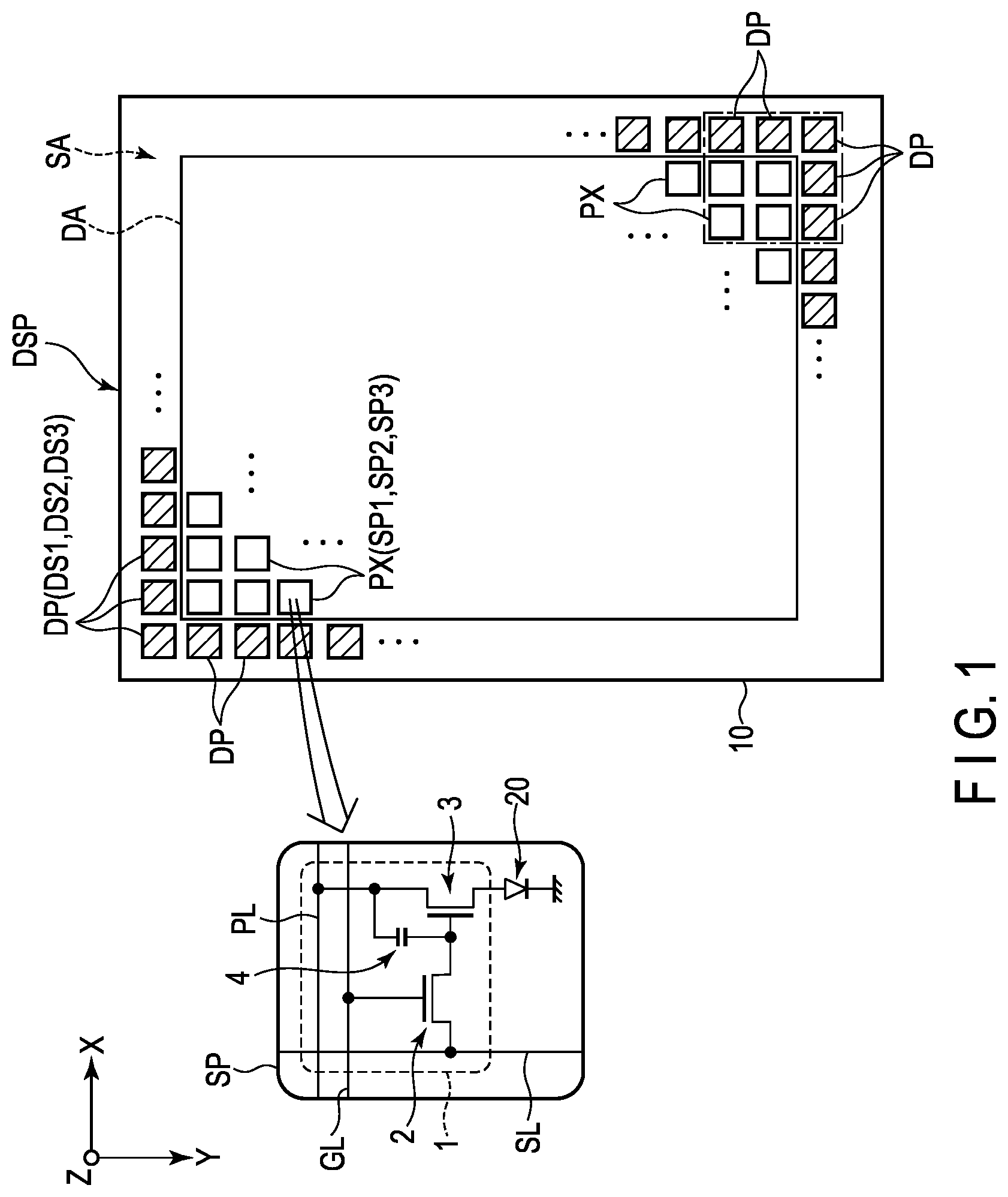
shows a configuration example of a display device DSP according to the first embodiment. The display device DSP includes a display area DA which displays images and a peripheral area SA on an outer side of the display area DA, on an insulating base 10 . The base 10 may be glass or a flexible resin film.
The display area DA comprises a plurality of pixels PX arranged in a matrix along the first direction X and the second direction Y. Each pixel PX comprises a plurality of sub-pixels SP. For example, the pixel PX comprises a red sub-pixel SP 1 , a green sub-pixel SP 2 , and a blue sub-pixel SP 3 . Note that, in addition to the three color sub-pixels, the pixel PX may include four or more sub-pixels of other colors, such as white and the like.
Each sub-pixel SP comprises a pixel circuit 1 and a display element 20 that is driven and controlled by the pixel circuit 1 . The pixel circuit 1 comprises a pixel switch 2 , a drive transistor 3 and a capacitor 4 . The pixel switch 2 and the drive transistor 3 are switching elements each formed of for example, a thin-film transistor.
In the pixel switch 2 , the gate electrode is connected to a respective scanning line GL, the source electrode is connected to a respective signal line SL, and the drain electrode is connected to one of the electrodes which constitute the capacitor 4 and the gate electrode of the drive transistor 3 . In the drive transistor 3 , the source electrode is connected to the other electrode of the capacitor 4 and a respective power line PL, and the drain electrode is connected to the anode of the display element 20 . Note that the configuration of the pixel circuit 1 is not limited to that of the example illustrated in the figure.
The display element 20 is an organic light-emitting diode (OLED) as a light-emitting element. For example, a sub-pixel SP 1 comprises a display element that emits light corresponding to a red wavelength, a sub-pixel SP 2 comprises a display element that emits light corresponding to a green wavelength, and a sub-pixel SP 3 comprises a display element that emits light corresponding to a blue wavelength. The configuration of the display elements 20 will be described later.
The peripheral area SA comprises a plurality of dummy pixels DP that do not display images. For example, the dummy pixels DP surrounds the display area DA. In other words, the dummy pixels DP are located between those pixels PX located on the outermost circumference and each side of the base 10 .
The dummy pixels DP each comprise a plurality of dummy sub-pixels DS. For example, each dummy pixel DP comprises a dummy sub-pixel DS 1 having a configuration similar to that of the sub-pixel SP 1 , a dummy sub-pixel DS 2 having a configuration similar to that of the sub-pixel SP 2 , and a dummy sub-pixel DS 3 having a configuration similar to that of the sub-pixel SP 3 .
shows an example of the layout of the sub-pixels SP 1 , SP 2 and SP 3 and the dummy sub-pixels DS 1 , DS 2 and DS 3 . Here, four pixels PX enclosed by a single-dotted frame and five dummy pixels DP located therearound as shown in will be focused.
In each of the pixels PX, sub-pixels SP 1 and SP 2 are aligned along the second direction Y, sub-pixels SP 1 and SP 3 are aligned along the first direction X, and sub-pixels SP 2 and SP 3 are aligned along the first direction X. The sub-pixel SP 1 is formed into substantially a rectangular shape extending along the first direction X. The sub-pixels SP 2 and SP 3 are each formed into substantially a rectangular shape extending along the second direction Y. The area of the sub-pixel SP 2 is greater than the area of the sub-pixel SP 1 , and the area of the sub-pixel SP 3 is greater than the area of the sub-pixel SP 2 . Note that the area of the sub-pixel SP 1 may be the same as that of the sub-pixel SP 2 .
Now, let us focus on those pixels PX arranged in the display area DA, the sub-pixels SP 1 and the sub-pixels SP 3 are alternately aligned along the first direction X. The sub-pixels SP 2 and the sub-pixels SP 3 are also alternately aligned along the first direction X. The sub-pixels SP 1 and the sub-pixels SP 2 are alternately aligned along the second direction Y. The sub-pixels SP 3 are aligned along the second direction Y without interposing the sub-pixels SP 1 and SP 2 .
The dummy sub-pixels DS 1 have the same shape as that of the sub-pixels SP 1 , the dummy sub-pixels DS 2 have the same shape as that of the sub-pixels SP 2 , and the dummy sub-pixels DS 3 have the same shape as that of the sub-pixels SP 3 . The arrangement of the dummy sub-pixels DS 1 , DS 2 and DS 3 in each dummy pixel DP is the same as that of the sub-pixels SP 1 , SP 2 and SP 3 in each pixel PX. The shape and arrangement of the dummy sub-pixels DS 1 , DS 2 and DS 3 may be different from the shape and arrangement of the sub-pixels SP 1 , SP 2 and SP 3 .
Note that the outlines of the sub-pixels SP 1 , SP 2 and SP 3 and the dummy sub-pixels DS 1 , DS 2 and DS 3 shown in correspond to the outlines of the pixel electrodes or the light-emitting area of the display device, but they are shown in a simplified form and do not necessarily reflect the actual shape.
is a schematic cross-sectional view of the display device DSP taken along line in . The display device DSP comprises an insulating layer 11 (first insulating layer) disposed on the base 10 and an insulating layer 12 (second insulating layer) disposed on the insulating layer 11 . The pixel circuit 1 and other components shown in are disposed on the base 10 and covered by the insulating layer 11 , illustration of which is omitted. The insulating layers 11 and 12 are, for example, organic insulating layers. The insulating layer 11 may be referred to as an underlayer of the display element 20 . The insulating layer 12 is formed to partition the display element 20 or the sub-pixel SP, and may be referred to as ribs or partition walls.
As in the sub-pixel SP 3 shown in , the display element 20 of each sub-pixel SP comprises a pixel electrode PE 1 (first pixel electrode), an organic layer OR 1 (first organic layer) and a common electrode CE. The pixel electrode PE 1 is an electrode provided for each sub-pixel SP or each display element 20 , and may be referred to as an upper electrode or anode. The common electrode CE is an electrode commonly provided for a plurality of sub-pixels SP or a plurality of display elements 20 , and may be referred to as a counter electrode, upper electrode or cathode.
The pixel electrode PE 1 is disposed on the insulating layer 11 , and its peripheral portion is covered by the insulating layer 12 . The pixel electrode PE 1 is electrically connected to the drive transistor 3 shown in . The pixel electrode PE 1 is a transparent electrode formed of, for example, a transparent conductive material such as indium tin oxide (ITO) or indium zinc oxide (IZO). Note that the pixel electrode PE 1 may also be a metal electrode formed of a metal material such as silver, aluminum or the like. Further, the pixel electrode PE 1 may be of a stacked body of transparent electrode and metal electrode. For example, the pixel electrode PE 1 may be configured as a stacked body in which a transparent electrode, a metal electrode and a transparent electrode are stacked in this order, or may be configured as a stacked body of three or more layers.
The insulating layer 12 comprises an opening OP superimposed on the pixel electrode PE 1 in each sub-pixel SP. The organic layer OR 1 is disposed on the insulating layer 12 and is in contact with the pixel electrode PE 1 through the opening OP.
is a cross-sectional view showing an example of a layer configuration that can be applied to the organic layer OR 1 . For example, the organic layer OR 1 includes a functional layer F 1 (first functional layer), a light-emitting layer EL and a functional layer F 2 (second functional layer), which are stacked in order from the pixel electrode PE 1 towards the common electrode CE. The functional layers F 1 and F 2 each are, for example, a hole injection layer, a hole transport layer, a hole blocking layer, an electron injection layer, an electron transport layer or an electron blocking layer, but may be other functional layers. Each of the functional layers F 1 and F 2 is not limited to a single layer, but as well be a stacked body in which multiple functional layers are stacked on one another. Further, at least one of the functional layers F 1 and F 2 may be omitted.
As shown in , the common electrode CE covers the organic layer OR 1 . The common electrode CE is a transparent electrode formed of, for example, a transparent conductive material such as ITO or IZO. The common electrode CE may be covered by a transparent protective film (including at least one of an inorganic insulating film and an organic insulating film).
When the potential of the pixel electrode PE 1 is relatively higher than that of the common electrode CE, the pixel electrode PE 1 corresponds to the anode and the common electrode CE corresponds to the cathode. On the other hand, when the potential of the common electrode CE is relatively higher than that of the pixel electrode PE 1 , the common electrode CE corresponds to the anode and the pixel electrode PE 1 corresponds to the cathode.
For example, when the pixel electrode PE 1 corresponds to the anode, the functional layer F 1 includes at least one of the hole injection layer and the hole transport layer, and the functional layer F 2 includes at least one of the electron transport layer and the electron injection layer.
As in the dummy sub-pixels DS 1 and DS 3 shown in , the dummy sub-pixels DS each include a pixel electrode PE 2 (second pixel electrode) and an organic layer OR 2 (second organic layer). As in the case of the pixel electrode PE 1 , the pixel electrode PE 2 is disposed on the insulating layer 11 and is covered by the insulating layer 12 . The pixel electrode PE 2 is formed by the same process and of the same material as those of the pixel electrode PE 1 . As in the case of the organic layer OR 1 , the organic layer OR 2 is disposed on the insulating layer 12 and is covered by the common electrode CE. The organic layer OR 2 has the same structure as that of the organic layer OR 1 , and for example, it contains the light-emitting layer EL and the functional layers F 1 and F 2 .
In the example illustrated in , the insulating layer 12 does not comprise an opening in the dummy sub-pixels DS. Therefore the pixel electrode PE 2 and the organic layer OR 2 of each dummy sub-pixel DS oppose each other via the insulating layer 12 . In the dummy sub-pixels DS with such a configuration, even if a potential difference is created between the pixel electrode PE 2 and the common electrode CE, the organic layer OR 2 does not emit light.
The dummy sub-pixels DS may comprise a pixel circuit 1 similar to that of the sub-pixels SP. This pixel circuit 1 may or may not be connected to the pixel electrode PE 2 . When the dummy sub-pixel DS comprises the pixel circuit 1 , this pixel circuit 1 can protect the pixel circuit 1 of the sub-pixel SP from electrostatic discharge which may be generated in the manufacturing process of the display device DSP, etc.
Between the organic layers OR 1 disposed respectively on two adjacent sub-pixels SP, between the organic layer OR 1 disposed on a sub-pixels SP and the organic layer OR 2 disposed on a dummy sub-pixel DS adjacent to this sub-pixels SP and between the organic layers OR 2 disposed respectively on two adjacent dummy sub-pixels DS, partition walls PT are respectively provided. In the example illustrated in , a dummy sub-pixel is placed between two dummy sub-pixels. In the example shown in , a partition wall PT is placed on a right side of the dummy sub-pixel DS 3 as well. The partition walls PT each are, for example, an organic insulating layer.
In the following descriptions, the four partition walls PT shown in may be referred to respectively as a partition wall PT 1 (first partition wall), a partition wall PT 2 (second partition wall), a partition wall PT 3 (third partition wall) and a partition wall PT 4 (fourth partition wall) in order from left to right. The partition walls PT 1 , PT 2 , PT 3 and PT 4 are disposed on the insulating layer 12 .
Each partition wall PT has a forward tapered shape. The forward tapered shape means such a shape as shown in the partition wall PT 1 shown in that a width W 1 of an upper portion is less than a width W 2 of a lower portion. Each side surface of the partition walls PT may be a plane inclined to the third direction Z, or it may be a curved surface. The partition wall PT may be configured to include a plurality of portions whose widths decrease in steps from the lower portion toward the upper portion.
The organic layer OR 1 of the sub-pixel SP 3 is located between the partition wall PT 1 and the partition wall PT 2 . The organic layer OR 2 of the dummy sub-pixel DS 1 is located between the partition wall PT 2 and the partition wall PT 3 . The organic layer OR 2 of the dummy sub-pixel DS 3 is located between the partition wall PT 3 and the partition wall PT 4 .
The common electrode CE continuously covers the organic layers OR 1 , OR 2 and the partition walls PT 1 , PT 2 , PT 3 and PT 4 . The common electrode CE is formed entirely over the area including the sub-pixels SP and dummy sub-pixels DS, for example, by vapor deposition. In the following descriptions, the portion of the common electrode CE, which covers the organic layer OR 1 may be referred to as the first portion P 1 , the portion which covers the organic layer OR 2 as the second portion P 2 , the portion which covers the upper portion of the partition wall PT as the third portion P 3 , and the portion located on an outer side of the partition wall PT (partition wall PT 4 ), which is located at an outermost end may be referred to as the fourth portion P 4 . In this embodiment, the first portion P 1 , the second portion P 2 , the third portion P 3 and the fourth portion P 4 are connected together.
The display device DSP further comprises a conductive layer CL 1 (first conductive layer) disposed between the insulating layers 11 and 12 , and a conductive layer CL 2 (second conductive layer) disposed between the base 10 and the insulating layer 11 . In the peripheral area SA, the insulating layer 12 comprises a contact hole CH 1 (first contact hole) and the insulating layer 11 comprises a contact hole CH 2 (second contact hole). For example, the conductive layer CL 1 is formed by the same process and of the same material as those of the pixel electrodes PE 1 and PE 2 .
The fourth portion P 4 of the common electrode CE is in contact with the conductive layer CL 1 via the contact hole CH 1 . The conductive layer CL 1 is in contact with the conductive layer CL 2 via the contact hole CH 2 . A common voltage is supplied to the conductive layer CL 2 . The common voltage is supplied to the entire common electrode CE via the conductive layer CL 1 .
In the example shown in , an organic layer OR 3 (third organic layer) is disposed between the partition wall PT 4 and the contact hole CH 1 . The organic layer OR 3 is disposed on the insulating layer 12 and covered by the fourth portion P 4 . For example, in the organic layers OR 1 and OR 2 , the light-emitting layers EL are each formed separately for the respective color of the sub-pixel SP and dummy sub-pixel DS. On the other hand, at least some of the layers contained in the functional layers F 1 and F 2 described above are formed at the same time entirely for the area including the sub-pixels SP and the dummy sub-pixels DS. For example, the organic layer OR 3 is a part where the layer (common layer) formed at the same time for each sub-pixel SP and each dummy sub-pixel DS as just mentioned, is divided by the partition wall PT 4 . In this case, the organic layer OR 3 may not necessarily contain the light-emitting layer EL.
The organic layer OR 1 of the sub-pixel SP 3 includes a first end portion E 1 on a side of the partition wall PT 1 and a second end portion E 2 on a side of the partition wall PT 2 . The first end portion E 1 and the second end portion E 2 are located above the insulating layer 12 .
is an enlarged schematic cross-sectional view showing the vicinity of the second end portion E 2 . The partition wall PT 2 includes an upper surface SF 1 and a side surface SF 2 . The second end portion E 2 is in contact with the side surface SF 2 .
In the example shown in , end portions of the light-emitting layer EL and the functional layers F 1 and F 2 are in contact with the side surface SF 2 . The common electrode CE continuously covers the functional layer F 2 , the side surface SF 2 and the upper surface SF 1 . The common electrode CE is not in contact with the light-emitting layer EL and the functional layer F 1 .
Note that at least part of the layers which constitute the organic layer OR 1 may be disposed on the upper surface SF 1 while the part being separated from the second end portion E 2 . For example, when the light-emitting layer EL and the functional layers F 1 and F 2 are formed in the area overlapping the partition wall PT 2 , part of the light-emitting layer EL and the functional layers F 1 and F 2 can be placed between the upper surface SF 1 and the common electrode CE. If the inclination of the side surface SF 2 is steep, such part is divided from the light-emitting layer EL and the functional layers F 1 and F 2 formed near the partition wall PT 2 .
The relationship between the first end portion E 1 and the partition wall PT 1 is similar to the relationship between the second end portion E 2 and the partition wall PT 2 . In other words, the first end portion E 1 is in contact with a side surface of the partition wall PT 1 . Further, both end portions of the organic layer OR 2 of the dummy sub-pixel DS 1 shown in are in contact with the respective side surfaces of the partition walls PT 2 and PT 3 and both end portions of the organic layer OR 2 of the dummy sub-pixel DS 3 are in contact with the respective side surfaces of the partition walls PT 3 and PT 4 .
is a schematic plan view of the pixel electrodes PE 1 , PE 2 and the organic layers OR 1 , OR 2 and OR 3 . The pixel electrodes PE 1 are spaced apart from each of the sub-pixels SP 1 , SP 2 and SP 3 . The pixel electrodes PE 1 overlap the above-described openings OP, respectively. The pixel electrodes PE 2 are spaced apart from each of the dummy sub-pixels DS 1 , DS 2 and DS 3 .
The organic layers OR 1 overlaps the pixel electrodes PE 1 respectively in the sub-pixels SP 1 , SP 2 and SP 3 . In the example shown in , a continuous organic layer OR 1 is provided for a plurality of sub-pixels SP 3 aligned along the second direction Y.
The organic layers OR 2 overlap the pixel electrodes PE 2 , respectively, in the dummy sub-pixels DS 1 , DS 2 and DS 3 . In the example shown in , a continuous organic layer OR 2 is provided for a plurality of dummy sub-pixels DS 3 aligned along the second direction Y. The organic layer OR 2 of the dummy sub-pixel DS 3 located adjacent to a sub-pixel SP 3 along the second direction Y is connected to the organic layer OR 1 of the sub-pixel SP 3 .
The organic layer OR 3 includes a portion extending along the first direction X and a portion extending along the second direction Y. For example, the organic layer OR 3 is formed in a ring shape in the peripheral area SA. The dummy sub-pixels DS 1 , DS 2 and DS 3 are located between the display area DA and the organic layer OR 3 .
is a schematic plan view of the partition walls PT, a common electrode CE and conductive layers CL 1 and CL 2 . The partition walls PT includes partition walls PTx extending along the first direction X and partition walls PTy extending along the second direction Y. The partition walls PT 1 , PT 2 , PT 3 and PT 4 shown in are all partition walls PTy.
The partition walls PTx and PTy are disposed between two adjacent sub-pixels SP, between two adjacent dummy sub-pixels DS and between adjacent pairs of respective sub-pixels SP and respective dummy sub-pixels DS, and are formed into a grid pattern as a whole. Note that the partition walls PTx may not be provided between two sub-pixels SP 3 aligned along the second direction Y, between two dummy sub-pixels DS 3 aligned along the second direction Y, and between adjacent pairs of respective sub-pixels SP 3 and respective dummy sub-pixels DS 3 aligned along the second direction Y.
For example, the conductive layers CL 1 and CL 2 are formed into a ring shape in the peripheral area SA. The dummy sub-pixels DS 1 , DS 2 and DS 3 are located between the display area DA and the conductive layers CL 1 and CL 2 .
In the example shown in , a large number of contact holes CH 1 and CH 2 are formed around the dummy sub-pixels DS 1 , DS 2 and DS 3 . The contact holes CH 1 are located closer to the side of the display area DA than the contact holes CH 2 . As another example, the contact holes CH 1 may have an elongated shape in which a plurality of contact holes CH 1 aligned along the first direction X or those aligned along the second direction Y in are connected together into one. Similarly, the contact holes CH 2 may have an elongated shape in which a plurality of contact holes CH 2 aligned along the first direction X or those aligned along the second direction Y in are connected together into one.
As indicated by the dashed lines in , the common electrode CE is disposed in the area including the sub-pixels SP 1 , SP 2 and SP 3 and the dummy sub-pixels DS 1 , DS 2 and DS 3 . An edge of the common electrode CE is located between the contact holes CH 1 and CH 2 .
shows the cross-sectional structure of the sub-pixels SP 3 and the dummy sub-pixels DS 1 and DS 3 along the first direction X. The cross-sectional structure of the sub-pixels SP 1 and SP 2 along the first direction X is also similar to that of the sub-pixel SP 3 , and the cross-sectional structure of the dummy sub-pixel DS 2 along the first direction X is also similar to that of the dummy sub-pixel DS 1 . Further, the cross-sectional structure of the sub-pixels SP 1 , SP 2 , and SP 3 along the second direction Y is similar to that of the sub-pixel SP 3 in , and the cross-sectional structure of the dummy sub-pixels DS 1 , DS 2 , and DS 3 along the second direction Y is similar to that of the dummy sub-pixels DS 1 and DS 3 in .
Of the elements disposed in the sub-pixels SP in the display area DA, for example, the pixel electrodes PE 1 are patterned by etching. When multiple elements are formed at the same time by etching, the outermost circumferential ones of these elements may be excessively eroded. Therefore, if there is no conductive layer similar to the pixel electrodes PE 1 on an outer side of the outermost pixel electrodes PE 1 in the display area DA, the pixels PX including the outermost pixel electrodes PE 1 cannot be formed to have a configuration as designed, and the display quality may be degraded.
In contrast, in this embodiment, the dummy pixels DP including the pixel electrodes PE 2 are disposed on an outer side of the outermost pixels PX in the display area DA. With this structure, excessive erosion of the pixel electrodes PE 1 of the outermost pixels PX does not easily occur, and as a result, the display quality of the display device DSP can be improved.
Further, in this embodiment, the partition walls PT are placed at boundaries of the sub-pixels SP and dummy sub-pixels SP, and the end portions of the organic layers OR 1 are respectively brought into contact with the side surfaces of the partition walls PT. One of the advantageous effects of this configuration will be explained below.
is a schematic cross-sectional view of a display device of a comparative example with respect to this embodiment, showing the vicinity of the end portion E of the organic layer OR 1 as in . The comparative example is different from the structure in in that partition walls PT are not provided. The second end portion E 2 is located above the insulating layer 12 and is covered by the common electrode CE.
In the comparative example, the light-emitting layer EL and the functional layer F 1 are in contact with the common electrode CE at the end portion E. Therefore, unlike the original current path through the functional layer F 1 , the light-emitting layer EL and the functional layer F 2 , a leak path LP is formed that directly connects the functional layer F 1 and the light-emitting layer EL to the common electrode CE. The leak path LP thus formed can cause a degradation in display quality and an increase in power consumption.
In particular, when a single mask is used to form each layer of the organic layer OR 1 , the material of each layer is also deposited at an edges of the opening of the mask; therefore the later the layer is formed, the slightly smaller, the size becomes. Thus, as shown in , the end portion E is inclined and the contact area between each layer of the organic layer OR 1 and the common electrode CE increases, which makes the formation of the leak path LP easy.
In contrast, when the end portion of the organic layer OR 1 is in contact with the side surface of each partition wall PT as in this embodiment, the light-emitting layer EL and the functional layer F 1 are not easily exposed from the functional layer F 2 . Therefore, the formation of the leakage path is suppressed, which makes it possible to improve the display quality of the display device DSP and to reduce the power consumption.
Apart from the above, various other advantageous effects can be obtained from this embodiment.
Second Embodiment
The second embodiment will now be described. Note that the configuration not specifically referred to here is similar to that of the first embodiment.
is a schematic cross-sectional view of an example of a display device DSP of this embodiment. is a schematic cross-sectional view of another example of the display device DSP according to this embodiment. In these figures, the common electrode CE comprises a first layer L 1 and a second layer L 2 . The first layer L 1 and the second layer L 2 are formed of, for example, a transparent conductive material such as ITO or IZO.
The first layer L 1 covers organic layers OR 1 , OR 2 , OR 3 , partition walls PT 1 , PT 2 , PT 3 , PT 4 and an insulating layer 12 around a contact hole CH 1 . The second layer L 2 covers the first layer L 1 . In this embodiment, a first portion P 1 , a second portion P 2 , a third portion P 3 and a fourth portion P 4 of the common electrode CE each include the first layer L 1 and the second layer L 2 .
In the example shown in , the first layer L 1 in the first portion P 1 , the second portion P 2 , the third portion P 3 and the fourth portion P 4 are continuously connected. Further, the second layer L 2 is continuously provided in the first portion P 1 , the second portion P 2 , the third portion P 3 and the fourth portion P 4 .
In the example shown in , the first layer L 1 in the first portion P 1 is separated from the first layer L 1 in the third portion P 3 , the first layer L 1 in the second portion P 2 is separated from the first layer L 1 in the third portion P 3 , and the first layer L 1 in the fourth portion P 4 is separated from the first layer L 1 in the third portion P 3 . On the other hand, the second layer L 2 is continuously provided in the first portion P 1 , second portion P 2 , third portion P 3 and fourth portion P 4 .
When the common electrode CE is thin, there is a possibility that the common electrode CE may break due to the steps formed by the partition wall PT and the opening OP as in the case of the first layer L 1 in . On the other hand, due to limitations of the manufacturing equipment, it may not be possible to make the transparent conductive layer, which is a single layer, sufficiently thick. However, as in this embodiment, when the common electrode CE is formed of two layers, the continuity of the entire common electrode CE can be maintained just in case where one layer is broken as in the example shown in by the other layer connected.
is a schematic cross-sectional view of still another example of the display device DSP of this embodiment. In the example illustrated in this figure, the first layer L 1 is formed in the display area DA, but not in the peripheral area SA. The second layer L 2 is formed in both the display area DA and the peripheral area SA.
With this configuration, the first portion P 1 and the third portion P 3 above the partition wall PT 1 include both the first layer L 1 and the second layer L 2 , but the second portion P 2 , the fourth portion P 4 and the third portion P 3 above the partition walls PT 2 , PT 3 and PT 4 contain the second layer L 2 and do not contain the first layer L 1 . In this configuration, the thickness of the first portion P 1 is greater than the thickness of the second portion P 2 .
When no opening OP is provided in the dummy sub-pixel DS, there are fewer stepped portions in the peripheral area SA, which makes the common electrode CE less breakable. Therefore, even in a configuration where the common electrode CE is multilayered in the display area DA and not multilayered in the peripheral area SA as in the example shown in , a sufficient effect of improving the conductivity of the common electrode CE can be obtained.
Third Embodiment
The third embodiment will now be described. The configuration that is not specifically referred to here is similar to that of the first embodiment.
is a schematic cross-sectional view of a display device DSP of this embodiment. In this embodiment, a power feed line FL is disposed on each partition wall PT. The power feed line FL is formed of a metal material. In the following descriptions, the four power feed lines FL shown in may be referred to as a power feed line FL 1 (first power feed line), a power feed line FL 2 (second power feed line), a power feed line FL 3 (third power feed line) and a power feed lines FLs, in order from left to right.
The power feed line FL 1 is disposed above the partition wall PT 1 . The power feed line FL 2 is disposed above the partition wall PT 2 . The power supply line FL 3 is disposed on the partition wall PT 3 . The power feed line FLs is located on the partition wall PT 4 . The power feed line FLs is wider than the power feed lines FL 1 , FL 2 and FL 3 and overlaps the contact hole CH 1 .
In the example shown in , the common electrode CE is divided by the partition walls PT 1 , PT 2 , PT 3 and PT 4 . More specifically, the first portion P 1 , the second portion P 2 , the third portion P 3 and the fourth portion P 4 of the common electrode CE are separated from each other.
The power supply line FL 1 is in contact with two first portions P 1 located on respective sides of the partition wall PT 1 . The power feed line FL 2 is in contact with the first portion P 1 and the second portion P 2 located on respective sides of the partition wall PT 2 . The power feed line FL 3 is in contact with two second portions P 2 located on respective sides of the partition wall PT 3 . The power feed line FLs is in contact with the second portion P 2 and the fourth portion P 4 located on respective sides of the partition wall PT 4 . The third portion P 3 is located between the partition wall PT 1 and the power feed line FL 1 , between the partition wall PT 2 and the power feed line FL 2 , between the partition wall PT 3 and the power feed line FL 3 , and between the partition wall PT 4 and the power feed line FLs.
is a schematic plan view of the partition walls PT, the power feed lines FL, the common electrode CE and the conductive layers CL 1 and CL 2 . The shapes of the partition walls PT, the common electrode CE and the conductive layers CL 1 , CL 2 are similar to those of the example shown in .
The power feed lines FL include power feed lines FLx extending along the first direction X and power feed lines FLy extending along the second direction Y. The power feed line FLx are respectively disposed above the partition walls PTx, and the power feed lines FLy are respectively disposed above the partition walls PTy. The power feed lines FL 1 , FL 2 and FL 3 shown in are all power feed lines FLy. The power feed lines FLs are formed into a ring shape in the peripheral area SA. The end portions of the power feed lines FLx and FLy are connected to the power feed lines FLs.
Thus, in this embodiment, the metal-made power feed lines FLs are disposed in the area including the sub-pixels SP and the dummy sub-pixels DS. With this configuration, it possible to reduce the resistance of the common electrode CE. Further, even if the common electrode CE is divided at the locations of the partition walls PT as in the example shown in , the common voltage can be well supplied to the display element 20 of each sub-pixel SP by connecting the divided portions by the power feed lines FL.
In each of the above embodiments, the layout and configuration of the pixels PX and dummy pixels DP are not limited to those shown in . For example, in each pixel PX, the sub-pixels SP (SP 1 , SP 2 and SP 3 ) of the same shape may be aligned along the first direction X. Similarly, in each dummy pixel DP, the dummy sub-pixels DS (DS 1 , DS 2 and DS 3 ) of the same shape may be aligned along the first direction X. In , dummy pixels DP are arranged only one circumference around the display area DA, but they may be arranged two or more times.
Note that , 10 and 11 each illustrate a case where the common electrode CE is formed of two layers, but the common electrode CE may be formed of three or more layers. If a single layer can be made thick, the common electrode CE may be formed thick, not from multiple layers.
In the configurations shown in , 9 , 10 and 11 , the power feed lines FL shown in may be provided.
The second portions P 2 disposed in the dummy sub-pixels DS may not be connected to the third portions P 3 or the power supply lines FL, respectively. In this case, the second portions P 2 may be floating.
In the configuration shown in , each of the third portion P 3 may not include the first layer L 1 . Further, in the configuration shown in , the third portion P 3 above the partition wall PT 1 may not include the first layer L 1 . Further, in the configuration shown in , the third portion P 3 may not be disposed between each partition wall PT and each respective power feed line FL.
Based on the display device which has been described in the above-described embodiments, a person having ordinary skill in the art may achieve a display device with an arbitral design change; however, as long as they fall within the scope and spirit of the present invention, such a display device shall be encompassed by the scope of the present invention.
A skilled person would conceive various changes and modifications of the present invention within the scope of the technical concept of the invention, and naturally, such changes and modifications are encompassed by the scope of the present invention. For example, if a skilled person adds/deletes/alters a structural element or design to/from/in the above-described embodiments, or adds/deletes/alters a step or a condition to/from/in the above-described embodiment, as long as they fall within the scope and spirit of the present invention, such addition, deletion, and altercation are encompassed by the scope of the present invention.
Further, regarding the present embodiments, any advantage and effect those will be obvious from the description of the specification or arbitrarily conceived by a skilled person are naturally considered achievable by the present invention.
Figures (12)
Citations
This patent cites (22)
- US8044582
- US9006969
- US2004/0160170
- US2008/0100209
- US2009/0009069
- US2009/0309489
- US2015/0060823
- US2017/0352708
- US2018/0315802
- US2019/0165085
- US2019/0393284
- US2019/0393445
- US2020/0013834
- US2020/0208259
- US2022/0157899
- US2000-195677
- US2004-207217
- US2008-047515
- US2008-135325
- US2009-032673
- US2010-118191
- US2012155987