Abstract
A display panel and a display apparatus. The display panel comprises: a first display region (R 1 ); a second display region (R 2 ), which is at least located on one side of the first display region (R 1 ); a plurality of sub-pixels, which are located in the first display region (R 1 ) and the second display region (R 2 ); a plurality of pixel groups (P 1 ), which are located in the first display region (R 1 ), at least one of the plurality of pixel groups (P 1 ) comprising at least two sub-pixels; and a first power line ( 311 ), which is configured to supply a first voltage signal (ELVDD) to a pixel circuit, the first power line ( 311 ) comprising a plurality of first conducting wires (L 1 ) and a plurality of second conducting wires (L 2 ), with at least one of the plurality of first conducting wires (L 1 ) comprising a first sub-wiring (L 111 ) extending in a first direction (D 1 ) and a second sub-wiring (L 112 ) extending in a second direction (D 2 ), and the second sub-wiring (L 112 ) being electrically connected to at least one of the plurality of second conducting wires (L 2 ). By means of the display panel, the mesh structure of a first power line can be more stable, and the voltage drop on the first power line is reduced, such that the brightness uniformity of the display panel is better.
Claims (17)
1. A display panel, comprising: a first display region; a second display region, at least located on a side of the first display region; a plurality of sub-pixels, located in the first display region and the second display region, a density of the sub-pixels in the first display region being less than a density of the sub-pixels in the second display region, and each of the plurality of the sub-pixels comprising a pixel circuit; a plurality of pixel groups, located in the first display region, at least one of the plurality of pixel groups comprising at least two sub-pixels; and a first power line, configured to provide a first voltage signal to the pixel circuit, wherein the first power line comprises a plurality of first wires and a plurality of second wires, the plurality of first wires extend to the first display region from the second display region and are electrically connected with the plurality of pixel groups, the plurality of second wires are located in the first display region and located between the adjacent first wires, the plurality of second wires extend along a first direction, the adjacent second wires are spaced from each other along the first direction, and the plurality of second wires are electrically connected with the plurality of pixel groups, wherein at least one of the plurality of first wires comprises a first sub-wire extending along the first direction and a second sub-wire extending along a second direction, the first direction intersects with the second direction, and the second sub-wire is electrically connected with at least one of the plurality of second wires, wherein the at least two sub-pixels comprise a first sub-pixel and a second sub-pixel, the first sub-pixel and the second sub-pixel are arranged along the first direction, at least one of the plurality of second wires is electrically connected with the first sub-pixel and the second sub-pixel, and the second sub-wire and the plurality of second wires are located in different layers, each of the plurality of the sub-pixels further comprises a light-emitting element, the pixel circuit comprises a first transistor, a second transistor, and a storage capacitor, the first transistor is respectively connected with the second transistor and the storage capacitor, the second transistor is connected with the light-emitting element, the first transistor comprises a first active part and a second active part, and the first active part and the second active part are connected by a conductive part, each of the plurality of the second wires further comprises a connecting arm, the connecting arm and the conductive part of one sub-pixel overlapping with the second wire in the pixel group are spaced from each other in a third direction and partially overlap in the third direction, and the third direction is perpendicular to the first direction and perpendicular to the second direction.
Show 16 dependent claims
2. The display panel according to claim 1 , wherein the plurality of pixel groups comprise a plurality of first pixel groups and a plurality of second pixel groups arranged at intervals, and the adjacent first pixel group and second pixel group are connected through a plurality of lines.
3. The display panel according to claim 2 , further comprising a connecting wire, orthogonal projections of at least two of the plurality of lines between the adjacent first pixel group and second pixel group on a base substrate falling within an orthogonal projection of the connecting wire on the base substrate.
4. The display panel according to claim 3 , wherein a plurality of gaps are formed between the plurality of lines, and an orthogonal projection of at least one of the plurality of gaps on the base substrate at least partially overlaps with the orthogonal projection of the connecting wire on the base substrate.
5. The display panel according to claim 2 , wherein the pixel circuit comprises a first reset signal line, a second reset signal line, a gate line, a light-emitting control signal line, and an initialization signal line, to respectively provide a first reset signal, a second reset signal, a gate electrode scanning signal, a light-emitting control signal, and an initialization signal to the pixel circuit; and the plurality of lines are selected from at least two of the first reset signal line, the second reset signal line, the gate line, the light-emitting control signal line, the initialization signal line, and the first wire.
6. The display panel according to claim 3 , wherein the connecting wire is provided with a block, and the block and the connecting wire are arranged in the same layer and integrally formed; the sub-pixel further comprises a light-emitting element, the pixel circuit includes a first transistor, a second transistor, and a storage capacitor, the first transistor is respectively connected with the second transistor and the storage capacitor, the second transistor is connected with the light-emitting element, the first transistor comprises a first active part and a second active part, and the first active part and the second active part are connected through a conductive part; and the block and the conductive part of one pixel unit overlapping with the first wire in the pixel group are spaced from each other in the third direction and partially overlap in the third direction.
7. The display panel according to claim 5 , wherein the orthogonal projection of the connecting wire on the base substrate is at least partially located between orthogonal projections of the adjacent first pixel group and second pixel group on the base substrate.
8. The display panel according to claim 7 , wherein a first reset signal line, a second reset signal line, a gate line, a light-emitting control signal line, an initialization signal line, and a second wire of the first pixel group are respectively connected with a first reset signal line, a second reset signal line, a gate line, a light-emitting control signal line, an initialization signal line, and a second wire of the second pixel group through the plurality of lines.
9. The display panel according to claim 8 , wherein the connecting wire and the second wire are located in the same layer and integrally formed; or the connecting wire and the initialization signal line are located in the same layer and integrally formed; or the connecting wire and the first wire are located in the same layer.
10. The display panel according to claim 1 , wherein the at least two sub-pixels further comprise a third sub-pixel and a fourth sub-pixel, the third sub-pixel and the fourth sub-pixel are arranged along the first direction and located on a side of the first sub-pixel and the second sub-pixel along the second direction, the third sub-pixel and the fourth sub-pixel are electrically connected with another one of the plurality of second wires, and the second sub-wire is electrically connected with at least one of the plurality of second wires.
11. The display panel according to claim 1 , wherein the second sub-wire is provided with a block, the block and the second sub-wire are located in different layers and connected by a through hole, and the block and the conductive part of one pixel unit overlapping with the first wire in the pixel group are spaced from each other in the third direction and partially overlap in the third direction.
12. The display panel according to claim 1 , wherein the plurality of second wires are sequentially arranged along the first direction, wherein the adjacent second wires are not directly connected.
13. The display panel according to claim 1 , wherein the first power line further comprises a third wire and a fourth wire, the third wire extends along the second direction, the third wire extends to the first display region from the second display region, and the second wire is electrically connected with the third wire; and the fourth wire extends along the second direction, the second wire is electrically connected with the fourth wire, and a length of the fourth wire in the second direction is less than or equal to a length of the third wire in the second direction.
14. The display panel according to claim 1 , comprising a plurality of fourth wires, the plurality of fourth wires being located between the adjacent third wires, the plurality of fourth wires being sequentially arranged along the second direction, and the adjacent fourth wires being spaced from each other in the second direction.
15. The display panel according to claim 2 , wherein the first display region comprises a plurality of light-transmitting regions located between adjacent pixel groups of the plurality of pixel groups, wherein the plurality of pixel groups and lines of the plurality of the lines connected with the adjacent pixel groups surround the plurality of light-transmitting regions.
16. A display device, comprising the display panel according to claim 1 .
17. The display device according to claim 16 , further comprising a sensor, wherein the sensor is arranged on a side of the display panel, and an orthogonal projection of the sensor on the base substrate at least partially overlaps with the first display region.
Full Description
Show full text →
The present disclosure is a national stage entry of a PCT patent application No. PCT/CN2021/094378, filed May 18, 2021, which claims priority of Chinese Patent Application No. 202010621890.3 filed on Jun. 30, 2020, the disclosure of which is incorporated herein by reference in its entirety as part of the present disclosure.
TECHNICAL FIELD
At least one embodiment of the present disclosure relates to a display panel and a display device.
BACKGROUND
Based on the design of a camera under panel, a display panel generally includes a high Pixels Per Inch (PPI) region and a low PPI region, but generally, the display panel has a relatively low light transmittance in the low PPI region, which is not beneficial for improving the display effect of the camera in an imaging region.
SUMMARY
At least one embodiment of the present disclosure provides a display panel, the display panel comprises: a first display region; a second display region, at least located on a side of the first display region; a plurality of sub-pixels, located in the first display region and the second display region, a density of the sub-pixels in the first display region being less than a density of the sub-pixels in the second display region, and each of the plurality of the sub-pixel comprising a pixel circuit; a plurality of pixel groups, located in the first display region, at least one of the plurality of pixel groups comprising at least two sub-pixels; and a first power line, configured to provide a first voltage signal to the pixel circuit, the first power line comprises a plurality of first wires and a plurality of second wires, the plurality of first wires extend to the first display region from the second display region and are electrically connected with the plurality of pixel groups, the plurality of second wires are located in the first display region and located between the adjacent first wires, the plurality of second wires extend along a first direction, the adjacent second wires are spaced from each other along the first direction, and the plurality of second wires are electrically connected with the plurality of pixel group, and at least one of the plurality of first wires comprises a first sub-wire extending along the first direction and a second sub-wire extending along a second direction, the first direction intersects with the second direction, and the second sub-wire is electrically connected with at least one of the plurality of second wires.
For example, in the display panel provided by at least one embodiment of the present disclosure, the at least two sub-pixels comprise a first sub-pixel and a second sub-pixel, the first sub-pixel and the second sub-pixel are arranged along the first direction, at least one of the plurality of second wires is electrically connected with the first sub-pixel and the second sub-pixel, and the second sub-wire and the plurality of second wires are located in different layers.
For example, in the display panel provided by at least one embodiment of the present disclosure, the sub-pixel further comprises a light-emitting element, the pixel circuit comprises a first transistor, a second transistor, and a storage capacitor, the first transistor is respectively connected with the second transistor and the storage capacitor, the second transistor is connected with the light-emitting element, the first transistor comprises a first active part and a second active part, and the first active part and the second active part are connected by a conductive part.
For example, in the display panel provided by at least one embodiment of the present disclosure, the second wire further comprises a connecting arm, the connecting arm and the conductive part of one sub-pixel overlapping with the second wire in the pixel group are spaced from each other in a third direction and partially overlap in the third direction, and the third direction is perpendicular to the first direction and perpendicular to the second direction.
For example, in the display panel provided by at least one embodiment of the present disclosure, a shape of the connecting arm comprises a C shape.
For example, in the display panel provided by at least one embodiment of the present disclosure, the plurality of pixel groups comprise a plurality of first pixel groups and a plurality of second pixel groups arranged at intervals, and the adjacent first pixel group and second pixel group are connected through a plurality of lines.
For example, the display panel provided by at least one embodiment of the present disclosure further comprises a connecting wire, orthogonal projections of at least two of the plurality of lines between the adjacent first pixel group and second pixel group on a base substrate falling within an orthogonal projection of the connecting wire on the base substrate.
For example, in the display panel provided by at least one embodiment of the present disclosure, a plurality of gaps are formed between the plurality of lines, and an orthogonal projection of at least one of the plurality of gaps on the base substrate at least partially overlaps with the orthogonal projection of the connecting wire on the base substrate.
For example, in the display panel provided by at least one embodiment of the present disclosure, the pixel circuit comprises a first reset signal line, a second reset signal line, a gate line, a light-emitting control signal line, and an initialization signal line, to respectively provide a first reset signal, a second reset signal, a gate electrode scanning signal, a light-emitting control signal, and an initialization signal to the pixel circuit; and the plurality of lines are selected from at least two of the first reset signal line, the second reset signal line, the gate line, the light-emitting control signal line, the initialization signal line, and the first wire.
For example, in the display panel provided by at least one embodiment of the present disclosure, the connecting wire is provided with a block, and the block and the connecting wire are arranged in the same layer and integrally formed; the sub-pixel further comprises a light-emitting element, the pixel circuit includes a first transistor, a second transistor, and a storage capacitor, the first transistor is respectively connected with the second transistor and the storage capacitor, the second transistor is connected with the light-emitting element, the first transistor comprises a first active part and a second active part, and the first active part and the second active part are connected through a conductive part; and the block and the conductive part of one pixel unit overlapping with the first wire in the pixel group are spaced from each other in the third direction and partially overlap in the third direction.
For example, in the display panel provided by at least one embodiment of the present disclosure, the orthogonal projection of the connecting wire on the base substrate is at least partially located between orthogonal projections of the adjacent first pixel group and second pixel group on the base substrate.
For example, in the display panel provided by at least one embodiment of the present disclosure, a first reset signal line, a second reset signal line, a gate line, a light-emitting control signal line, an initialization signal line, and a second wire of the first pixel group are respectively connected with a first reset signal line, a second reset signal line, a gate line, a light-emitting control signal line, an initialization signal line, and a second wire of the second pixel group through the plurality of lines.
For example, in the display panel provided by at least one embodiment of the present disclosure, the connecting wire and the second wire are located in the same layer and integrally formed; or the connecting wire and the initialization signal line are located in the same layer and integrally formed; or the connecting wire and the first wire are located in the same layer.
For example, in the display panel provided by at least one embodiment of the present disclosure, the at least two sub-pixels further comprise a third sub-pixel and a fourth sub-pixel, the third sub-pixel and the fourth sub-pixel are arranged along the first direction and located on a side of the first sub-pixel and the second sub-pixel along the second direction, the third sub-pixel and the fourth sub-pixel are electrically connected with another one of the plurality of second wires, and the second sub-wire is electrically connected with at least one of the plurality of second wires.
For example, in the display panel provided by at least one embodiment of the present disclosure, the second sub-wire is provided with a block, the block and the second sub-wire are located in different layers and connected by a through hole, and the block and the conductive part of one pixel unit overlapping with the first wire in the pixel group are spaced from each other in the third direction and partially overlap in the third direction.
For example, in the display panel provided by at least one embodiment of the present disclosure, the first direction is perpendicular to the second direction.
For example, in the display panel provided by at least one embodiment of the present disclosure, the plurality of second wires are sequentially arranged along the first direction.
For example, in the display panel provided by at least one embodiment of the present disclosure, the adjacent second wires are not directly connected.
For example, in the display panel provided by at least one embodiment of the present disclosure, the first wire and the second wire are connected by a through hole penetrating through an insulating layer.
For example, in the display panel provided by at least one embodiment of the present disclosure, the first power line further comprises a third wire and a fourth wire, the third wire extends along the second direction, the third wire extends to the first display region from the second display region, and the second wire is electrically connected with the third wire; and the fourth wire extends along the second direction, the second wire is electrically connected with the fourth wire, and a length of the fourth wire in the second direction is less than or equal to a length of the third wire in the second direction.
For example, the display panel provided by at least one embodiment of the present disclosure comprises a plurality of fourth wires, the plurality of fourth wires being located between the adjacent third wires, the plurality of fourth wires being sequentially arranged along the second direction, and the adjacent fourth wires being spaced from each other in the second direction.
For example, in the display panel provided by at least one embodiment of the present disclosure, the first wire and the third wire are located in the same layer, and the fourth wire and the third wire are located in the same layer.
For example, in the display panel provided by at least one embodiment of the present disclosure, the first display region comprises a plurality of light-transmitting regions located between the adjacent pixel groups.
For example, in the display panel provided by at least one embodiment of the present disclosure, the plurality of pixel groups and the lines connected with the adjacent pixel groups surround the plurality of light-transmitting regions.
At least one embodiment of the present disclosure further provides a display device, the display device comprises the display panel provided by any embodiment of the present disclosure.
For example, the display panel provided by at least one embodiment of the present disclosure further comprises a sensor, the sensor is arranged on a side of the display panel, and an orthogonal projection of the sensor on the base substrate at least partially overlaps with the first display region.
BRIEF DESCRIPTION OF THE DRAWINGS
In order to clearly illustrate the technical solution of the embodiments of the present disclosure, the drawings of the embodiments will be briefly described in the following; it is obvious that the described drawings are only related to some embodiments of the invention and thus are not limitative of the invention.
A to C are schematic diagrams of a display panel provided by some embodiments of the present disclosure;
is a schematic diagram of a second display region of a display panel provided by at least one embodiment of the present disclosure;
is a schematic diagram of a first display region of a display panel provided by at least one embodiment of the present disclosure;
is a schematic diagram of a sub-pixel and a signal line for providing a signal to the sub-pixel in a display panel provided by at least one embodiment of the present disclosure;
is a schematic diagram of a display panel provided by at least one embodiment of the present disclosure;
A to F are diagrams of a pixel circuit and a laminated structure thereof provided by some embodiments of the present disclosure;
is a schematic diagram of a display panel provided by at least one embodiment of the present disclosure;
A is an enlarged schematic diagram of a region A 11 shown in ;
B is an enlarged schematic diagram of a region A 12 shown in ;
C is a plan view of a semiconductor pattern of the display panel shown in ;
is a plan view of a first conductive pattern layer of the display panel shown in ;
is a plan view of a second conductive pattern layer of the display panel shown in ;
is a plan view of a third conductive pattern layer of the display panel shown in ;
is a plan view of another display panel provided by at least one embodiment of the present disclosure;
is an enlarged schematic diagram of a region A 21 shown in ;
is a plan view of a semiconductor pattern of the display panel shown in ;
is a plan view of a first conductive pattern layer of the display panel shown in ;
is a plan view of a second conductive pattern layer of the display panel shown in ;
is a plan view of a third conductive pattern layer of the display panel shown in ;
is a schematic diagram of yet another display panel provided by at least one embodiment of the present disclosure;
is a plan view of a semiconductor pattern of the display panel shown in ;
is a plan view of a first conductive pattern layer of the display panel shown in ;
is a plan view of a second conductive pattern layer of the display panel shown in ;
is a plan view of a third conductive pattern layer of the display panel shown in ;
is a cross-sectional schematic diagram of a pixel circuit of a display panel provided by at least one embodiment of the present disclosure;
is a cross-sectional schematic diagram of a display panel provided by at least one embodiment of the present disclosure; and
is a schematic diagram of a display device provided by at least one embodiment of the present disclosure.
DETAILED DESCRIPTION
In order to make objects, technical details and advantages of the embodiments of the invention apparent, the technical solutions of the embodiment will be described in a clearly and fully understandable way in connection with the drawings related to the embodiments of the invention. It is obvious that the described embodiments are just a part but not all of the embodiments of the invention. Based on the described embodiments herein, those skilled in the art can obtain other embodiment(s), without any inventive work, which should be within the scope of the invention.
Unless otherwise defined, all the technical and scientific terms used herein have the same meanings as commonly understood by one of ordinary skill in the art to which the present disclosure belongs. The terms, such as “first,” “second,” or the like, which are used in the description and the claims of the present disclosure, are not intended to indicate any sequence, amount or importance, but for distinguishing various components. The terms, such as “comprise/comprising,” “include/including,” or the like are intended to specify that the elements or the objects stated before these terms encompass the elements or the objects and equivalents thereof listed after these terms, but not preclude other elements or objects. The terms, such as “connect/connecting/connected,” “couple/coupling/coupled” or the like, are not limited to a physical connection or mechanical connection, but may include an electrical connection/coupling, directly or indirectly. The terms, “on,” “under,” “left,” “right,” or the like are only used to indicate relative position relationship, and when the position of the object which is described is changed, the relative position relationship may be changed accordingly.
Due to people's love for selfie, a front camera hole has to exist, but the front camera hole and a sensor may occupy a portion of space, and at present, methods for placing the front camera hole include: a notch screen or a waterdrop screen is adopted; or an Active Area (AA) hole is adopted, i.e., the AA is performed a hole digging, and the camera and the sensor are integrally placed in the AA. However, such two methods both cannot meet the requirements of a full screen. Therefore, we select to adopt the camera under screen technology, the aperture ratio of the screen is improved through changing the Pixels Per Inch (PPI), and the camera is placed under the screen, so that the display completeness of the overall screen cannot be damaged.
In order to implement the frameless full screen design, the camera under screen technology has to be adopted, and it needs to improve the aperture ratio of a display panel. Therefore, on the premise of achieving the requirement above, how to arrange the structure of the display panel to ensure the display effect of the display panel becomes the problem which urgently needs to be solved.
At least one embodiment of the present disclosure provides a display panel, including: a first display region; a second display region, which is at least located on a side of the first display region; a plurality of sub-pixels, which are located in the first display region and the second display region, the density of the sub-pixels in the first display region being less than that of the sub-pixels in the second display region, and the sub-pixel including a pixel circuit; a plurality of pixel groups, which are located in the first display region, at least one of the plurality of pixel groups including at least two sub-pixels; and a first power line, which is configured to provide a first voltage signal to the pixel circuit. The first power line includes a plurality of first wires and a plurality of second wires, the plurality of first wires extend to the first display region from the second display region and are electrically connected with the plurality of pixel groups, the plurality of second wires are located in the first display region and located between the adjacent first wires, the plurality of second wires extend along a first direction, the adjacent second wires are spaced from each other along the first direction, and the plurality of second wires are electrically connected with the plurality of pixel groups; and at least one of the plurality of first wires includes a first sub-wire extending along the first direction and a second sub-wire extending along a second direction, the first direction intersects with the second direction, and the second sub-wire is electrically connected with at least one of the plurality of second wires.
The display panel provided by the embodiments of the present disclosure can make a net-shaped structure of the first power line more stable and reduce the voltage drop of the first power line, so as to make the brightness uniformity of the display panel better, thereby improving the display effect of a camera in an imaging region.
The embodiments of the present disclosure will be illustrated in detail below in combination with the drawings.
In a common display panel, no matter in a high PPI region or a low PPI region, the first power line always adopts the net-shaped structure. In order to make the net-shaped structure of the first power line more stable and reduce the voltage drop of the first power line so as to make the brightness uniformity of the display panel better, thereby improving the display effect of the camera in the imaging region, according to the display panel provided by the embodiments of the present disclosure, a signal line in the low PPI region is optimized, and for example, according to the embodiments of the present disclosure, wires of the net-shaped first power line, which are arranged transversely and longitudinally, are optimized.
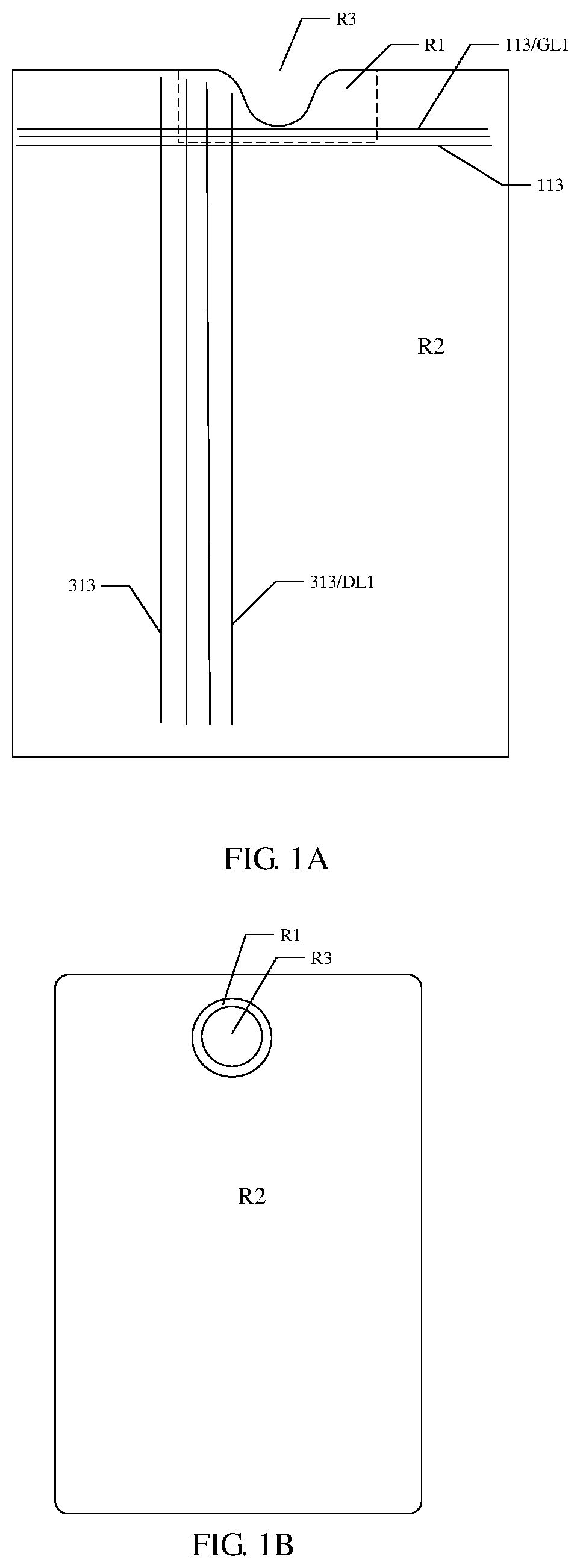
A to C are schematic diagrams of a display panel provided by some embodiments of the present disclosure. As shown in A to C , the display panel includes a first display region R 1 and a second display region R 2 . The first display region R 1 is a low PPI region, and the second display region R 2 is a high PPI region. The first display region R 1 is a partial light-transmitting region. As shown in A to C , the second display region R 2 is at least located on a side of the first display region RE The display panel shown in A and B further includes a third region R 3 . A sensor, e.g., a camera, may be arranged in the first display region R 1 (as shown in C ), or arranged in the first display region R 1 and the third region R 3 (as shown in A and B ). The third region R 3 shown in A and B may be a perforated region, i.e., a material at the position corresponding to the third region R 3 is removed to form a through hole. The sensor can receive ambient light. By taking a case that the sensor is the camera as an example, a camera under the screen is implemented, so that when a screen is normally used, the first display region corresponding to the sensor can normally display an image, and when the camera carries out shooting, the first display region can transmit the ambient light to support normal use. For example, the sensor is arranged on a non-display side of the display panel. The sensor may also be called as a member under screen.
A also shows a plurality of gate lines 113 and a plurality of data lines 313 . The plurality of gate lines 113 include a first gate line GL 1 , and the plurality of data lines 313 include a first data line DL 1 . The first gate line GL 1 extends to the first display region R 1 from the second display region R 2 . The first data line DL 1 extends to the second display region R 2 from the first display region RE In the embodiments of the present disclosure, extension of a certain element from first display region R 1 to the second display region R 2 may be understood as a case that the element is located in the first display region R 1 and the second display region R 2 , or may be regarded as extension of the certain element from the second display region R 2 to the first display region RE For diagram clarity, A schematically shows several gate lines 113 and several data lines 313 , and the numbers of the gate lines 113 and the data lines 313 may be determined as required. A plurality of gate lines 113 and a plurality of data lines 313 interact with each other and insulated from each other.
is a schematic diagram of a second display region of a display panel provided by at least one embodiment of the present disclosure. is a schematic diagram of a first display region of a display panel provided by at least one embodiment of the present disclosure. As shown in and , the display panel includes a plurality of sub-pixels P 0 , and the plurality of sub-pixels P 0 include a first sub-pixel 101 , a second sub-pixel 102 , a third sub-pixel 103 , and a fourth sub-pixel 104 . For example, the display panel includes a plurality of pixel groups P 1 located in the first display region R 1 , and at least one of the plurality of pixel groups P 1 includes at least two sub-pixels. For example, in some examples, one pixel group P 1 may include four sub-pixels, and for example, as shown in , one first sub-pixel 101 , one second sub-pixel 102 , one third sub-pixel 103 , and one fourth sub-pixel 104 constitute one pixel group P 1 ; for example, in some another examples, one pixel group P 1 may include two sub-pixels, and for example, as shown in , one first sub-pixel 101 and one second sub-pixel 102 constitute one pixel group P 1 ; and for example, one pixel group P 1 may also include three sub-pixels (as shown in ), and the embodiments of the present disclosure do not make any limit thereto. For example, one pixel group P 1 is one repeat unit, and the pixel groups P 1 are arranged in an array in the second display region R 2 . As shown in , in the first display region R 1 , one pixel group P 1 is also called as one pixel island P 1 , which is the same in the embodiments below and is not repeated. The first display region R 1 includes a plurality of light-transmitting regions R 0 ; and the light-transmitting regions R 0 are located between the adjacent pixel islands P 1 . The light-transmitting region R 0 can transmit the ambient light. For example, the light-transmitting region R 0 may include a base substrate and a transparent insulating layer located on the base substrate, and the light-transmitting region R 0 is not provided with a light-shielding structure and for example, is not provided with a metal wire. For example, the light-transmitting region R 0 is located in a region surrounded by four adjacent pixel islands P 1 , but the present disclosure is not limited thereto. For example, as shown in , the adjacent pixel islands P 1 are arranged at intervals.
For example, the length of each of the plurality of light-transmitting regions R 0 is substantially the same with that of one sub-pixel. For example, the pixel groups and the wires connected with the adjacent pixel groups surround the plurality of light-transmitting regions R 0 .
For example, in an example shown in , one pixel island may also include two sub-pixels and for example, include a first sub-pixel 101 and a second sub-pixel 102 , and for example, the first sub-pixel 101 is a red sub-pixel and the second sub-pixel 102 is a green sub-pixel; for example, in an embodiment shown in , one pixel island P 1 may also include three sub-pixels and for example, include a first sub-pixel 101 , a second sub-pixel 102 , and a third sub-pixel 103 , for example, the first sub-pixel 101 is a red sub-pixel, the second sub-pixel 102 is a green sub-pixel, and the third sub-pixel is a blue sub-pixel, and for example, the three sub-pixels are located in one row; and for example, in an example shown in , one pixel island P 1 may also include four sub-pixels and for example, include a first sub-pixel 101 , a second sub-pixel 102 , a third sub-pixel 103 , and a fourth sub-pixel 104 , for example, the first sub-pixel 101 is a red sub-pixel, the second sub-pixel 102 is a green sub-pixel, the third sub-pixel is a blue sub-pixel, and the fourth sub-pixel 104 is a green sub-pixel, and in other embodiments, the pixel group may also adopt other colors of pixel units. Certainly, in other embodiments, an arrangement mode of the plurality of sub-pixels P 0 in the display panel is also limited to those shown in and . The embodiments of the present disclosure do not make any limit thereto.
With reference to and , the plurality of sub-pixels P 0 are located in the first display region R 1 and the second display region R 2 , the density of the pixel units in the first display region R 1 is less than that of the pixel units in the second display region R 2 . Or, the density of the sub-pixels in the first display region R 1 is less than that of the sub-pixels in the second display region R 2 . The density of the pixel units in the first display region R 1 shown in is a quarter of the density of the pixel units in the second display region R 2 . Namely, the density of the sub-pixels in the first display region R 1 shown in is a quarter of the density of the sub-pixels in the second display region R 2 . An arrangement mode of the light-transmitting regions R 0 and the pixel units in the first display region R 1 is not limited to that shown in , and may be set as required. For example, in other embodiments, the density of the sub-pixels in the first display region R 1 is one second, one third, one sixth or one eighth, and the like of the density of the sub-pixels in the second display region R 2 , which is different from the value of one quarter, and the embodiments of the present disclosure do not make any limit thereto.
For example, as shown in A and , the display panel further includes the gate line 113 and the data line 313 . The gate line 113 and the data line 313 are insulated from each other. Each gate line 113 is connected with one row of sub-pixels, and each data line 313 is connected with one column of sub-pixels. For example, the gate line 113 is configured to provide a scanning signal to one row of sub-pixels.
For example, as shown in A and , the data line 313 includes the first data line DL 1 . The first data line DL 1 is at least located in the first display region R 1 . For example, the first data line DL 1 extends to the second display region R 2 from the first display region R 1 .
For example, as shown in A and , the gate line includes the first gate line GL 1 , and the first gate line GL 1 extends to the first display region R 1 from the second display region R 2 . As shown in , the light-transmitting region R 0 is formed in a surrounding mode by two adjacent first gate lines GL 1 and two adjacent first data lines DL 1 , but the present disclosure is not limited thereto.
is a schematic diagram of a sub-pixel and a signal line for providing a signal to the sub-pixel in a display panel provided by an embodiment of the present disclosure. As shown in , the display panel includes a plurality of sub-pixels P 0 , each sub-pixel P 0 includes a light-emitting element EMC and a pixel circuit 10 for providing a driving current to the light-emitting element EMC, and the light-emitting element EMC may be an electroluminescent element, e.g., an organic electroluminescent element, and for example, may be an Organic Light-Emitting Diode (OLED).
As shown in , the display panel further includes an initialization signal line 210 , a light-emitting control signal line 110 , a data line 313 , a first power line 311 , and a second power line 312 . For example, the gate line 113 is configured to provide a scanning signal SCAN to the pixel circuit 10 . The light-emitting control signal line 110 is configured to provide a light-emitting control signal EM to the sub-pixel P 0 . The data line 313 is configured to provide a data signal DATA to the pixel circuit 10 , the first power line 311 is configured to provide a constant first voltage signal ELVDD to the pixel circuit, the second power line 312 is configured to provide a constant second voltage signal ELVSS to the pixel circuit 10 , and the first voltage signal ELVDD is greater than the second voltage signal ELVSS. The initialization signal line 210 is configured to provide an initialization signal Vint to the pixel circuit 10 . The initialization signal Vint is a constant voltage signal, the magnitude of the initialization signal Vint, for example, may be between the first voltage signal ELVDD and the second voltage signal ELVSS, but the present disclosure is not limited thereto, and for example, the initialization signal Vint may be less than or equal to the second voltage signal ELVSS. For example, the pixel circuit 10 outputs a driving current under the control of signals such as the scanning signal SCAN, the data signal DATA, the initialization signal Vint, the first voltage signal ELVDD, the second voltage signal ELVSS, the light-emitting control signal EM, and the like so as to drive the light-emitting element EMC to emit light. As shown in , the light-emitting element EMC includes a pixel electrode E 1 and a common electrode E 2 . The pixel electrode E 1 is connected with the pixel circuit 10 , and the common electrode E 2 is connected with the second power line 312 .
is a schematic diagram of a display panel provided by some embodiments of the present disclosure. It should be noted that illustration is carried out in by taking a case that one pixel island P 1 includes two sub-pixels as an example, each pixel island P 1 may also include three or four sub-pixels, the specific connection relationship of the three or four sub-pixels is similar with that of two sub-pixels and is not repeated herein, and the embodiments of the present disclosure do not make any limit thereto.
As shown in , the first power line 311 includes a plurality of first wires L 1 and a plurality of second wires L 2 . For example, the first power line 311 may also include a plurality of third wires L 3 . For example, the first wire L 1 extends to the first display region R 1 from the second display region R 2 , and is electrically connected with a plurality of pixel groups (i.e., pixel islands) P 1 . The plurality of second wires L 2 are located in the first display region R 1 and located between the adjacent first wires L 1 , each second wire L 2 extends along the first direction D 1 , and the plurality of second wires L 2 are electrically connected with the plurality of pixel groups P 1 . For example, the third wire L 3 is at least located in the first display region R 1 , for example, the third wire L 3 extends to the first display region R 1 from the second display region R 2 , the third wire extends along the second direction D 2 , the first direction D 1 intersects with the second direction D 2 , the adjacent second wires L 2 are spaced from each other along the first direction D 1 , and the adjacent second wires L 2 are connected through the first wire L 1 and are connected with the third wire L 3 to receive the first voltage signal ELVDD. For example, the first direction D 1 is perpendicular to the second direction D 2 , but the present disclosure is not limited thereto. For example, the first wire L 1 extends along the first direction D 1 . For example, in the embodiments of the present disclosure, the second wire L 2 is merely located in the first display region RE In the embodiments of the present disclosure, an element extending along a certain direction is not necessarily of a straight line shape and may also have a curve line or broken line portion, for example, the extension direction of a certain element refers to the rough extension trend of the element, and for example, each portion of the element does not necessarily extend along this direction.
For example, as shown in , the first wires L 1 and the second wires L 2 are respectively connected with the sub-pixels in the two adjacent pixel islands P 1 , which are located in the corresponding rows, but the present disclosure is not limited thereto, and in other embodiments, the pixel island P 1 may also include two or more rows of sub-pixels. For example, as shown in A to E , the pixel island P 1 at least includes one row of two pixel units, the second wire L 2 overlaps with the one row of two pixel units. For example, as shown in , the first wire L 1 is located between the two adjacent pixel islands P 1 , and the second wire L 2 respectively overlapping with the two adjacent pixel islands P 1 is connected through the first wire L 1 .
For example, as shown in , a plurality of second wires L 2 are sequentially arranged along the first direction DE For example, as shown in , the adjacent second wires L 2 are not directly connected, for example, are connected in a jumper mode, i.e., are connected through the first wires L 1 located in different layers, so that the net-shaped structure of the first power line is more stable and the voltage drop of the first power line is reduced, thereby making the brightness uniformity of the display panel better. Certainly, the adjacent second wires L 2 may also be directly connected, and the embodiments of the present disclosure do not make any limit thereto.
For example, as shown in , in order to improve the light transmittance of the first display region, the length of a portion of the first wire L 1 , which is located in the first display region R 1 , in the first direction D 1 is greater than that of the second wire L 2 in the first direction D 1 .
For example, as shown in , the first power line 311 further includes a fourth wire L 4 , the fourth wire L 4 extends along the second direction D 2 , the second wire L 2 is connected with the fourth wire L 4 to receive the first voltage signal ELVDD, and the length of the fourth wire L 4 in the second direction D 2 is less than or equal to that of the three conductor L 3 in the second direction D 2 . In the display panel shown in , the length of the fourth wire L 4 in the second direction D 2 is less than that of the three conductor L 3 in the second direction D 2 .
For example, as shown in , in order to further improve the light transmittance of the first display region, a plurality of fourth wires L 4 are provided, the plurality of fourth wires L 4 are sequentially arranged along the second direction D 2 , and the adjacent fourth wires L 4 are spaced from each other in the second direction D 2 . For example, as shown in , the plurality of fourth wires L 4 are located between a third wire L 31 and a third wire L 32 , and the third wire L 31 and the third wire L 32 are the adjacent third wires L 3 . shows five fourth wires L 41 , but the number of the fourth wires L 4 located between the adjacent third wires L 3 is not limited to that shown in the drawing and may be determined as required. A plurality of fourth wires L 4 are spaced from each other in the second direction D 2 and equivalently, portions of some of first power lines arranged along the second direction in a common display panel are removed, so that wiring is reduced, the wire space is optimized, and the light transmittance is improved.
For example, as shown in , the first power line 311 further includes a fifth wire L 5 , the fifth wire L 5 extends along the first direction D 1 , the fifth wire L 5 is located in the second display region R 2 , and the fifth wire L 5 and the second wire L 2 adjacent to the fifth wire L 5 are spaced from each other along the first direction D 1 . Therefore, at the junction position of the first display region and the second display region, wiring is reduced and the light transmittance is improved.
In the embodiments of the present disclosure, the number of the pixel units included by each pixel island and an arrangement mode of the pixel units are not limited.
As shown in , in the display panel, the first power line 311 further includes a plurality of sixth wires L 6 , the sixth wires L 6 are located in the second display region R 2 , and the sixth wires L 6 extend along the second direction D 2 . In the second display region R 2 , the plurality of fifth conductors L 5 and the plurality of sixth wires L 6 interact with each other. In the embodiments of the present disclosure, both the fifth wires L 5 and the sixth wires L 6 are merely located in the second display region R 2 .
As shown in , the same gate line 113 connects the sub-pixels in the second display region, which are located on both sides of the first display region R 1 , and the sub-pixels located in the first display region R 1 to form one row of sub-pixels. The embodiments of the present disclosure do not make any limit to the form of the first wire, as long as the first wire can extend to the first display region R 1 from the second display region R 2 . The first power line in also may be replaced with the first power lines in other embodiments of the present disclosure. In addition, the extension mode of the gate line 113 is not limited to that shown in , as long as the arrangement mode of the gate line 113 can enable the pixels in the second display region R 2 and the pixels in the first display region R 1 to be connected. For example, in the first display region R 1 , the gate lines of the corresponding rows of sub-pixels between two adjacent pixel islands are connected through seventh wires L 7 (i.e., in a jumper mode), certainly, the gate lines of the corresponding rows of sub-pixels between two adjacent pixel islands may also be directly connected, and the embodiments of the present disclosure do not make any limit thereto.
For example, a corresponding relationship between the rest of signal lines (e.g., the initialization signal line for providing the initialization signal Vint and the light-emitting control signal line for providing the light-emitting control signal EM) and one pixel island P 1 is as shown in , the embodiments of the present disclosure do not make any limit thereto, and the corresponding relationship is not repeated herein.
For example, in the display panel shown in , the first wire is in contact with two adjacent second wires for example by a through hole passing through the insulating layer.
For example, in the embodiments of the present disclosure, one row of sub-pixels are sub-pixels connected to the same gate line 113 , while one row of sub-pixels are sub-pixels connected to the same data line 313 . In the embodiments of the present disclosure, illustration is carried out by taking a case that the first wire L 1 , the second wire L 2 , and the fifth wire L 5 all extend along a row direction (i.e., the first direction D 1 ) and the third wire L 3 , the fourth wire L 4 , and the sixth wire L 6 extend along a column direction (i.e., the second direction D 2 ) as an example, but the present disclosure is not limited thereto. In other embodiments, it may also be that the first wire L 1 , the second wire L 2 , and the fifth wire L 5 all extend along the column direction, the third wire L 3 , the fourth wire L 4 , and the sixth wire L 6 extend along the row direction, and correspondingly, the second direction D 2 and the first direction D 1 also may be replaced with each other.
takes a case that the pixel island includes two sub-pixels (e.g., one row of sub-pixels) as an example, in other embodiments, the pixel island may also include three or more sub-pixels (e.g., two rows of sub-pixels), and in this case, the plurality of second wires may be understood as the second wires connected with the same row of sub-pixels in one pixel island. In the case that the first wire L 1 , the second wire L 2 , and the fifth wire L 5 all extend along the column direction and the third wire L 3 , the fourth wire L 4 , and the sixth wire L 6 extend along the row direction, the plurality of second wires may be understood as the second wires connected with the same column of sub-pixels in one pixel island.
Some embodiments of the present disclosure will be described below in combination with A to . A to illustrate by taking a 7T1C pixel circuit as an example.
A is a schematic diagram of a pixel circuit of a display panel provided by an embodiment of the present disclosure. B is a plan view of a semiconductor pattern in a display panel provided by an embodiment of the present disclosure. C is a plan view of a first conductive pattern layer in a display panel provided by an embodiment of the present disclosure. D is a plan view of a second conductive pattern layer in a display panel provided by an embodiment of the present disclosure. is a cross-sectional schematic diagram of a display panel provided by an embodiment of the present disclosure. is a cross-sectional schematic diagram of a display panel provided by an embodiment of the present disclosure. In the embodiment, for illustration clarity, in the plan views, the insulating layer is shown in a form of the through hole, and the insulating layer adopts transparentizing processing.
It should be noted that B to F respectively show layered structure views of the pixel circuit including two sub-pixels. It should be noted that more or fewer sub-pixels may also be included, the structure of the pixel circuit may be designed by adopting a layout of one of the pixels shown in B to F , and the embodiments of the present disclosure do not make any limit thereto. For example, F illustrates by taking a pixel structure of the first sub-pixel 101 as an example, and pixel structures of the rest of sub-pixels, e.g., the second sub-pixel, the third sub-pixel, and the fourth sub-pixel, are similar with it and are not repeated herein.
For example, with reference to A , the gate line 113 is configured to provide the scanning signal SCAN to the pixel circuit 10 . The light-emitting control signal line 110 is configured to provide the light-emitting control signal EM to the sub-pixel P 0 . The data line 313 is configured to provide the data signal DATA to the pixel circuit 10 , the first power line 311 is configured to provide the constant first voltage signal ELVDD to the pixel circuit 10 , the second power line 312 is configured to provide the constant second voltage signal ELVSS to the pixel circuit 10 , and the first voltage signal ELVDD is greater than the second voltage signal ELVSS. The initialization signal line 210 is configured to provide the initialization signal Vint to the pixel circuit 10 . The initialization signal Vint is the constant voltage signal, the magnitude of the initialization signal Vint, for example, may be between the first voltage signal ELVDD and the second voltage signal ELVSS, but the present disclosure is not limited thereto, and for example, the initialization signal Vint may be less than or equal to the second voltage signal ELVSS. For example, the pixel circuit 10 outputs the driving current under the control of the scanning signal SCAN, the data signal DATA, the initialization signal Vint, the first voltage signal ELVDD, the second voltage signal ELVSS, the light-emitting control signal EM, and the like so as to drive the light-emitting element 20 to emit light. The light-emitting element 20 emit red light, blue light, green light, or white light, and the like under the drive of the corresponding pixel circuit 10 .
As shown in A , the pixel circuit 10 includes a driving transistor T 1 , a data writing transistor T 2 , a threshold compensation transistor T 3 , a first light-emitting control transistor T 4 , a second light-emitting control transistor T 5 , a first reset transistor T 6 , a second reset transistor T 7 , and a storage capacitor C 1 . The driving transistor T 1 is electrically connected with the light-emitting element 20 , and outputs the driving current under the control of the scanning signal SCAN, the data signal DATA, the first voltage signal ELVDD, the second voltage signal ELVSS, and the like to drive the light-emitting element 20 to emit light.
For example, a display panel provided by an embodiment of the present disclosure further includes: a data driving circuit and a scanning driving circuit. The data driving circuit is configured to provide the data signal DATA to the sub-pixel P 0 according to an instruction of a control circuit; and the scanning driving circuit is configured to provide a signal such as the light-emitting control signal EM, the scanning signal SCAN, a first reset control signal RST 1 , a second reset signal RST 2 , and the like to the sub-pixel P 0 according to an instruction of the control circuit. For example, the control circuit includes an external Integrated Circuit (IC), but the present disclosure is not limited thereto. For example, the scanning driving circuit is a Gate Driver On Array (GOA) structure mounted on the display panel, or is a driving chip (IC) structure bonded to the display panel. For example, different driving circuits may also be adopted to respectively provide the light-emitting control signal EM and the scanning signal SCAN. For example, the display panel further includes a power source (not shown in the figure) to provide the above voltage signal, the power source may be a voltage source or a current source as required, and the power source is configured to respectively provide the first voltage signal ELVDD, the second voltage signal ELVSS, the initialization signal Vint, and the like to the sub-pixel P 0 through the first power line 311 , the second power line 312 , and the initialization signal line 210 .
As shown in A , a second electrode C 12 of the storage capacitor C 1 is electrically connected with the first power line 311 , and a first electrode C 11 of the storage capacitor C 1 is electrically connected with a second electrode T 32 of the threshold compensation transistor T 3 . A gate electrode T 20 of the data writing transistor T 2 is electrically connected with the gate line 113 , and a first electrode T 21 and a second electrode T 22 of the data writing transistor T 2 are respectively and electrically connected with the data line 313 and a first electrode T 11 of the driving transistor T 1 . A gate electrode T 30 of the threshold compensation transistor T 3 is electrically connected with the gate line 113 , a first electrode T 31 of the threshold compensation transistor T 3 is electrically connected with a second electrode T 12 of the driving transistor T 1 , and the second electrode T 32 of the threshold compensation transistor T 3 is electrically connected with a gate electrode T 10 of the driving transistor T 1 .
For example, as shown in A , a gate electrode T 40 of the first light-emitting control transistor T 4 and a gate electrode T 50 of the second light-emitting control transistor T 5 are both connected with the light-emitting control signal line 110 .
For example, as shown in A , a first electrode T 41 and a second electrode T 42 of the first light-emitting control transistor T 4 are respectively and electrically connected with the first power line 311 and the first electrode T 11 of the driving transistor T 1 . A first electrode T 51 and a second electrode T 52 of the second light-emitting control transistor T 5 are respectively and electrically connected with the second electrode T 12 of the driving transistor T 1 and the pixel electrode E 1 (which may be an anode of an OLED) of the light-emitting element 20 . The common electrode E 2 (which may be a common electrode of the OLED, e.g., a cathode) of the light-emitting element 20 is electrically connected with the second power line 312 .
For example, as shown in A , a gate electrode T 60 of the first reset transistor T 6 is electrically connected with a first reset control signal line 111 , a first electrode T 61 of the first reset transistor T 6 is electrically connected with the initialization signal line 210 (a first initialization signal line 211 ), and a second electrode T 62 of the first reset transistor T 6 is electrically connected with the gate electrode T 10 of the driving transistor T 1 . A gate electrode T 70 of the second reset transistor T 7 is electrically connected with a second reset control signal line 112 , a first electrode T 71 of the second reset transistor T 7 is electrically connected with the initialization signal line 210 (a second initialization signal line 212 ), and a second electrode T 72 of the second reset transistor T 7 is electrically connected with the pixel electrode E 1 of the light-emitting element 20 .
B shows a semiconductor pattern SCP, C shows the first conductive pattern layer LY 1 , and a first gate insulating layer is arranged between the first conductive pattern layer LY 1 and the semiconductor pattern SCP. The semiconductor pattern SCP is doped by taking the first conductive pattern layer LY 1 as a mask, so that the semiconductor characteristic is reserved in a region of the semiconductor pattern SCP, which is not covered by the first conductive pattern layer LY 1 , a channel of a thin film transistor is formed, a region of the semiconductor pattern SCP, which is covered by the first conductive pattern layer LY 1 , is subjected to conductor treatment, and a source electrode or a drain electrode of the thin film transistor is formed. A shows an active layer ALT formed after the semiconductor pattern SCP is partially subjected to conductor treatment.
As shown in C , the first conductive pattern layer LY 1 includes the first reset control signal line 111 , the second reset control signal line 112 , the light-emitting control signal line 110 , the gate line 113 , and the first electrode C 11 of the storage capacitor C 1 . C further shows a first portion DL 11 (a wire 114 ) of the first data line DLL For example, with reference to , in the embodiments of the present disclosure, a current row of gate line 113 is also connected with the second reset control signal line 112 located in the same row.
D shows a second conducive pattern layer LY 2 , and a second gate insulating layer is arranged between the second conductive pattern layer LY 2 and the first conductive pattern layer LY 1 . The second conductive pattern layer LY 2 includes a block BK 0 , a block BK 1 , the initialization signal line 210 and the second electrode C 12 of the storage capacitor C 1 . The second electrodes C 12 of the storage capacitors C 1 of two sub-pixels of one pixel island are integrally formed to serve as the second wire L 2 . The second electrode C 12 of the storage capacitor C 1 has an opening OPN. An interlayer insulating layer is located between the second conductive pattern layer LY 2 and the third conductive pattern layer LY 3 . What is related to the first gate insulating layer, the second gate insulating layer, the interlayer insulating layer, the first conductive pattern layer LY 1 , the second conductive pattern layer LY 2 , and a third conductive pattern layer LY 3 may refer to illustration in the art, and will not be repeated herein.
E shows the third conductive pattern layer LY 3 , and the third conductive pattern layer LY 3 includes the first wire L 1 , the third wire L 3 (a portion of the first power line 311 ), the fourth wire L 4 (a portion of the first power line 311 ), a second portion DL 12 of the data line (a portion of the data line 313 ), a first connecting electrode 31 a , a second connecting electrode 31 b , a third connecting electrode 31 c , and a fourth connecting electrode 31 d.
For example, as shown in E , at least one of a plurality of first wires L 1 includes a first sub-wire L 111 extending along the first direction D 1 and a second sub-wire L 112 extending along the second direction D 2 , and the second sub-wire L 112 is electrically connected with at least one of a plurality of second wires L 2 . For example, as shown in , the second sub-wire L 112 is electrically connected with the corresponding row of second wire L 2 in the adjacent pixel islands. For example, as shown in and , the second sub-wire L 112 is electrically connected with two second wires L 2 in one pixel island and two second wires L 2 in the pixel island adjacent to the one pixel island. The embodiments of the present disclosure do not make any limit thereto.
For example, the second sub-wire L 112 is connected with the block BK 0 by a through hole passing through the interlayer insulating layer, and is connected with the second wire L 2 by a through hole passing through the interlayer insulating layer.
F is a diagram of a laminated structure of B to E . With reference to B to A , the data line 313 is electrically connected with the first electrode T 21 of the data writing transistor T 2 by a through hole, the first power line 311 is electrically connected with the first electrode T 41 of the first light-emitting control transistor T 4 by a through hole, the first power line 311 is electrically connected with the second electrode C 12 of the storage capacitor C 1 by a through hole, and the first power line 311 is electrically connected with a conductive block BK 1 by a through hole. An end of a first connecting electrode 31 a is electrically connected with the first initialization signal line 211 by a through hole, and another end of the first connecting electrode 31 a is connected with the first electrode T 61 of the first reset transistor T 6 by a through hole, so that the first electrode T 61 of the first reset transistor T 6 is electrically connected with the first initialization signal line 211 . An end of a second connecting electrode 31 b is electrically connected with the second electrode T 62 of the first reset transistor T 6 by a through hole, and another end of the second connecting electrode 31 b is electrically connected with the gate electrode T 10 of the driving transistor T 1 (i.e., the first electrode C 11 of the storage capacitor C 1 ) by a through hole, so that the second electrode T 62 of the first reset transistor T 6 is electrically connected with the gate electrode T 10 of the driving transistor T 1 (i.e., the first electrode C 11 of the storage capacitor C 1 ). An end of a third connecting electrode 31 c is electrically connected with the second initialization signal line 212 by a through hole, and another end of the third connecting electrode 31 c is connected with the first electrode T 71 of the second reset transistor T 7 by a through hole, so that the first electrode T 71 of the second reset transistor T 7 is electrically connected with the second initialization signal line 212 . A fourth connecting electrode 31 d is electrically connected with the second electrode T 52 of the second light-emitting control transistor T 5 by a through hole. The fourth connecting electrode 31 d may be used for being electrically connected with the pixel electrode E 1 (with reference to A ) of the light-emitting element 20 formed later. For example, the positional relationship of the first connecting electrode 31 a and the third connecting electrode 31 c may refer to positions in E , and for clarity and brevity, is not shown in F .
It should be illustrated that the transistors adopted in some embodiments of the present disclosure all may be thin film transistors, or field effect transistors, or other switching members with the same characteristics. The source electrode and the drain electrode of the transistor adopted herein may be symmetric in structure, so the source electrode and the drain electrode of the transistor structurally may have no difference. In one embodiment of the present disclosure, in order to distinguish two electrodes of the transistor except for the gate electrode, it is directly described that one electrode is the first electrode, and the other electrode is the second electrode, and thus, the first electrodes and the second electrodes of all or part of transistors in the embodiments of the present disclosure may be exchanged as required. For example, according to the embodiments of the present disclosure, the first electrode of the transistor may be the source electrode, while the second electrode may be the drain electrode; or, the first electrode of the transistor is the drain electrode, while the second electrode is the source electrode.
In addition, the transistors may be classified into N-type and P-type transistors according to the characteristics of the transistors. The embodiments of the present disclosure are illustrated by taking a case that all the transistors adopt the P-type transistors as an example. Based on the description and instruction of the present disclosure on this implementation mode, those ordinary skilled in the art, without any creative work, could easily think of a case that at least a portion of transistors in the pixel circuit according to the embodiments of the present disclosure adopt the N-type transistors, i.e., an N-type transistor or N-type transistor and P-type transistor combined implementation mode is adopted, and thus, these implementation modes also fall within the scope of protection of the present disclosure.
A to F illustrate by taking the 7T1C pixel circuit as an example, and the embodiments of the present disclosure include, but are not limited to it. It should be noted that the embodiments of the present disclosure do not make any limit to the number of the thin film transistors and the number of the capacitors included in the pixel circuit. For example, in some additional embodiments, the pixel circuit of the display panel may also be of a structure including other numbers of transistors, such as a 7T2C structure, a 6T1C structure, a 6T2C structure, or a 9T3C structure, which is not limited by the embodiments of the present disclosure.
is the cross-sectional schematic diagram of a pixel circuit of the display panel provided by some embodiment of the present disclosure. For example, as shown in , the display panel includes a thin film transistor 50 and a storage capacitor C 1 . The thin film transistor 50 includes an active layer ATL 1 located on the base substrate BS, a first gate insulating layer GI 1 located on a side of the active layer ATL 1 away from the base substrate BS, and a gate electrode GE located on a side of the first gate insulating layer GI 1 , which is away from the base substrate BS. The display panel further includes a second gate insulating layer GI 2 located on a side of the gate electrode GE, which is away from the base substrate BS, an interlayer insulating layer ILD located on a side of the second gate insulating layer GI 2 , which is away from the base substrate BS, and a source electrode or drain electrode CNE 1 located on a side of the interlayer insulating layer ILD, which is away from the base substrate BS. For example, when the thin film transistor 50 is implemented as the N-type transistor, CNE 1 represents the source electrode of the thin film transistor 50 and CNE 2 represents the drain electrode of the thin film transistor 50 ; and when the thin film transistor 50 is implemented as the P-type transistor, CNE 1 represents the drain electrode of the thin film transistor 50 and CNE 2 represents the source electrode of the thin film transistor 50 . The active layer ATL 1 includes a channel CN 11 and a first electrode ET 1 and a second electrode ET 2 respectively located on both sides of the channel CN 11 , and the connecting electrode CNE 1 is connected with the second electrode ET 2 by a through hole passing through the first gate insulating layer GIL the second gate insulating layer GI 2 , and the interlayer insulating layer ILD. The storage capacitor C 1 includes the first electrode C 11 and the second electrode C 12 , the first electrode C 11 and the gate electrode GE are located in the same layer and both are located in the first conductive pattern layer LY 1 , and the second electrode C 12 is located between the second gate insulating layer GI 2 and the interlayer insulating layer ILD and located in the second conductive pattern layer LY 2 . One of the first electrode ET 1 and the second electrode ET 2 is a source electrode, and the other one of the first electrode ET 1 and the second electrode ET 2 is a drain electrode. The connecting electrode CNE 1 is located in the third conductive pattern layer LY 3 . The display panel further includes a passivation layer PVX and a planarization layer PLN. For example, the source electrode or drain electrode CNE 1 is a first portion of the fourth connecting electrode 31 d shown in E or F , and the thin film transistor 50 may be the second light-emitting control transistor T 5 .
As shown in , the display panel further includes the light-emitting element EMC, the light-emitting element EMC includes the pixel electrode E 1 , a light-emitting functional layer EML, and the common electrode E 2 , and the pixel electrode E 1 is connected with the connecting electrode CNE 1 by a through hole penetrating through the passivation layer PVX and the planarization layer PLN. The display panel further includes an encapsulation layer CPS, and the encapsulation layer CPS includes a first encapsulation layer CPS 1 , a second encapsulation layer CPS 2 , and a third encapsulation layer CPS 3 . For example, the first encapsulation layer CPS 1 and the third encapsulation layer CPS 3 are inorganic material layers, and the second encapsulation layer CPS 2 is an organic material layer. For example, the pixel electrode E 1 is an anode, the common electrode E 2 is a cathode, but the present disclosure is not limited thereto.
For example, the light-emitting element EMC includes an Organic Light-Emitting Diode (OLED). The light-emitting functional layer is located between the common electrode E 2 and the pixel electrode E 1 . The light-emitting functional layer EML at least includes a light-emitting layer, and may further include at least one of a hole transport layer, a hole injection layer, an electron transport layer, and an electron injection layer.
As shown in , the display panel further includes a pixel definition layer PDL and a spacer PS. The pixel definition layer PDL has an opening, the opening is configured to define a light-emitting area (a light emergent region, an effective light-emitting area) of the pixel unit, and the spacer PS is configured to support a fine metal mask when the light-emitting functional layer EML is formed. shows that the spacers PS are arranged on both opposite sides of the light-emitting element, but the present disclosure is not limited thereto.
For example, the data line is configured to input the data signal to the pixel unit, and the first power line is configured to input the first voltage signal to the driving transistor. The second power line is configured to input the second voltage signal to the sub-pixel. The first voltage signal is a constant voltage, the second voltage signal is a constant voltage, for example, the first voltage signal is a positive voltage, the second voltage signal is a negative voltage, but the present disclosure is not limited thereto. For example, in some embodiment, the first voltage signal is the positive voltage, and the second power line is grounded.
With reference to , in the embodiment of the present disclosure, a first insulating layer ISL 1 includes at least one of the first gate insulating layer Gil, the second gate insulating layer GI 2 , and the interlayer insulating layer ILD, and a second insulating layer ISL 2 includes the planarization layer PLN.
For example, the first gate insulating layer Gil, the second gate insulating layer GI 2 , the interlayer insulating layer ILD, the passivation layer PVX, the planarization layer PLN, the pixel definition layer PDL, and the spacer PS are all made of an insulating material. For example, materials of the first gate insulating layer GI 1 , the second gate insulating layer GI 2 , the interlayer insulating layer ILD, and the passivation layer PVX include at least one of SiOx and SiNx, but are not limited thereto. For example, the planarization layer PLN, the pixel definition layer PDL, and the spacer PS may be made of an organic insulating material, e.g., resin, but the present disclosure is not limited thereto.
With reference to F , the threshold compensation transistor T 3 includes a first active part CN 1 and a second active part CN 2 , and the first active part CN 1 and the second active part CN 2 are connected through a conductive part CP. With reference to B and , the second wire L 2 further includes a connecting arm L 21 . The threshold compensation transistor T 3 is a double-gate transistor, when the threshold compensation transistor T 3 is turned off, the conductive part CP is in a floating state and is liable to jump due to influence of the voltage of a surrounding line, and the voltage jumping of the conductive part CP may influence the leakage current of the threshold compensation transistor T 3 so as to influence the light-emitting brightness of the pixel unit, and thus, the voltage of the conductive part CP needs to be kept stable. A block may be designed to form the capacitor with the conductive part CP, and the block may have a constant voltage signal, so that the voltage of the conductive part CP in the floating state is kept stable. The block BK 0 and the block BK 1 mentioned in the embodiments of the present disclosure and the connecting arm mentioned later all take an effect of stabilizing the voltage of the conductive part CP.
is a schematic diagram of a display panel provided by at least one embodiment of the present disclosure; A is an enlarged schematic diagram of a region A 11 shown in ; B is an enlarged schematic diagram of a region A 12 shown in ; C is a plan view of the semiconductor pattern of the display panel shown in ; is a plan view of the first conductive pattern layer of the display panel shown in ; is a plan view of the second conductive pattern layer of the display panel shown in ; and is a plan view of the third conductive pattern layer of the display panel shown in .
For example, as shown in , at least two sub-pixels include the first sub-pixel 101 and the second sub-pixel 102 , and the first sub-pixel 101 and the second sub-pixel 102 are arranged along the first direction D 1 . For example, as shown in A , at least one of a plurality of second wires L 2 is electrically connected with the first sub-pixel 101 and the second sub-pixel 102 , and the second sub-wire L 112 and the plurality of second wires L 2 are located in different layers.
For example, as shown in A , the sub-pixel P 0 further includes the light-emitting element 20 , the pixel circuit includes a first transistor (e.g., the threshold compensation transistor T 3 ) and a second transistor (e.g., the second light-emitting control transistor T 5 shown in A ), the first transistor T 3 is connected with the second transistor T 5 , and the second transistor T 5 is connected with the light-emitting element 20 . For example, as shown in F , the first transistor T 3 includes the first active part CN 1 and the second active part CN 2 , and the first active part CN 1 and the second active part CN 2 are connected through the conductive part CP.
For example, as shown in B and , the second wire L 2 further includes the connecting arm L 21 , the connecting arm L 21 and the conductive part CP of one sub-pixel in the pixel group, which overlaps with the second wire L 2 , are spaced from each other in a third direction D 3 and partially overlap in the third direction D 3 (with reference to ), and the third direction D 3 is perpendicular to the first direction D 1 and perpendicular to the second direction D 2 .
For example, as shown in B and , the shape of the connecting arm L 21 includes a C shape. It should be illustrated that the connecting arm L 21 may be substantially of a C shape, and certainly, the connecting arm L 21 may also adopt other shapes, as long as the connecting arm L 21 can take the effect of stabilizing the threshold compensation transistor T 3 .
With reference to , the connecting arm L 21 partially overlaps with the conductive part CP of the threshold compensation transistor T 3 to form a capacitor C 0 , and the first gate insulating layer GI 1 and the second gate insulating layer GI 2 are arranged between the connecting arm L 21 and the conductive part CP. further shows the second active part CN 2 . The capacitor C 0 may be called as a stabilization capacitor, and the connecting arm L 21 and the conductive part CP are two polar plates of the capacitor C 0 . As shown in , a gate electrode GE 2 overlaps with the second active part CN 2 in a direction perpendicular to the base substrate BS. The gate electrode GE 2 is a gate electrode of the threshold compensation transistor T 3 . As shown in , a portion of the second connecting electrode 31 b (as shown in E ) is used as the second electrode T 32 (e.g., the drain electrode) of the threshold compensation transistor T 3 .
For example, the third direction D 3 is perpendicular to the first direction D 1 and perpendicular to the second direction D 2 , the third direction D 3 is a direction perpendicular to the base substrate BS, and the first gate insulating layer GI 1 and the second gate insulating layer GI 2 are arranged between the connecting arm L 21 and the conductive part CP. For example, the first direction D 1 and the second direction D 2 are directions in parallel to a main surface of the base substrate BS, and the third direction D 3 is a direction perpendicular to the main surface of the base substrate BS. Various elements are produced on the main surface of the base substrate BS.
With reference to F , A , and , the block BK 0 and the conductive part of one sub-pixel in the pixel island, which overlaps with the first wire L 1 , are spaced from each other in the third direction D 3 and partially overlap in the third direction D 3 . With reference to F , A , and , the block BK 0 and the conductive part CP of one sub-pixel (the sub-pixel on the lower right corner in A ) in the pixel island, which overlaps with the first wire L 1 , are spaced from each other in the third direction D 3 and partially overlap in the third direction D 3 .
For example, with reference to A , F , B , and , the second wire L 2 further includes the connecting arm L 21 , the connecting arm L 21 and the conductive part CP of one sub-pixel (the sub-pixel located on the upper right corner in , i.e., the sub-pixel in B ) in the pixel island, which overlaps with the second wire L 2 , are spaced from each other in the third direction D 3 and partially overlap in the third direction D 3 . For example, the first transistor and the second transistor respectively are the threshold compensation transistor T 3 in the pixel circuit 10 and the light-emitting control transistor connected with the light-emitting element. For example, the light-emitting control transistor connected with the light-emitting element is the second light-emitting control transistor T 5 as above-mentioned. Certain, in other embodiments of the present disclosure, the block or the connecting arm forming the capacitor with the conductive part CP in the first transistor in the pixel island may also adopt other forms, which is not limited herein.
For example, as shown in D , the initialization signal line 20 includes a plurality of hollow regions HP, the second wire L 2 is located in one hollow region HP and is surrounded by a portion of the initialization signal line, which forms the hollow region HP in a surrounding mode, and the second wire L 2 does not overlap with the portion of the initialization signal line, which forms the hollow region in a surrounding mode. Namely, the second wire L 2 is completely surrounded by the portion of the initialization signal line, which forms the hollow region HP in a surrounding mode. In the embodiments of the present disclosure, the hollow region HP is a position corresponding to a removed portion of a thin film when the initialization signal line 210 is produced.
For example, with reference to A , the first wire L 1 includes the first sub-wire L 111 and the second sub-wire L 112 , the first sub-wire L 111 of the first wire L 1 is not located in the same layer with the second wire L 2 , and the second sub-wire L 112 of the first wire L 1 is not located in the same layer with the second wire L 2 . With reference to A , , and , the second wire L 2 is located in the second conductive pattern layer LY 2 , and the first wire L 1 is located in the third conductive pattern layer LY 3 .
For example, with reference to , the data line 313 includes the first data line DL 1 , and the first data line DL 1 extends to the second display region R 2 from the first display region R 1 . For example, as shown in A , the first portion DL 11 of the first data line DL 1 partially overlaps with an orthogonal projection of the third wire L 3 on the base substrate BS. Such setting mode is beneficial for reducing the wiring area and improving the light transmittance.
For example, with reference to C , D , , and A , the first data line DL 1 includes the first portion DL 11 and the second portion DL 12 , the first portion DL 11 of the first data line DL 1 partially overlaps with the third wire L 3 , the second portion DL 12 of the first data line DL 1 does not overlap with the third wire L 4 , and the first portion DL 11 of the first data line DL 1 and the second portion DL 12 of the first data line DL 1 are respectively located in different layers. For example, the first portion DL 11 (a wire 214 ) of the first data line DL 1 on the left side in A is located in the second conductive pattern layer, and the second portion DL 12 of the first data line DL 1 on the left side is located in the third conductive pattern layer, the first portion DL 11 (a wire 114 ) of the first data line DL 1 on the right side in A is located in the first conductive pattern layer shown in , and the second portion DL 12 of the first data line DL 1 on the right side in A is located in the third conductive pattern layer shown in . For example, with reference to , , and , the first portion DL 11 of the first data line DL 1 is located between the adjacent pixel islands P 1 .
For example, with reference to , two first data lines DL 1 are provided, and two first data lines DL 1 are respectively connected with two adjacent columns of sub-pixels. For example, as shown in A , the first portions DL 11 of two first data lines partially overlap with the orthogonal projection of the same third wire L 3 on the base substrate BS. Such setting mode enables the data line between the pixel islands in the two adjacent columns of sub-pixels to be hidden under the third conductor so as to reduce the wiring area and improve the light transmittance.
For example, the first wire L 1 and the second wire L 2 are located in different layers and connected by a through hole passing through the insulating layer. With reference to A and , the first wire L 1 is located in the third conductive pattern layer LY 3 , and the second wire is located in the second conductive pattern layer LY 2 . With reference to and , an interlayer dielectric layer ILD is arranged between the second conductive pattern layer LY 2 and the third conductive pattern layer LY 3 , i.e., the second sub-wire L 112 of the first wire L 2 and the second wire L 2 are connected by a through hole penetrating through the interlayer dielectric layer ILD.
For example, with reference to , the first wire and the third wire L 3 are located in the same layer and both located in the third conductive pattern layer LY 3 . The fourth wire L 4 and the third wire L 3 are located in the same layer and both located in the third conductive pattern layer LY 3 .
For example, a plurality of pixel groups include a plurality of first pixel groups (i.e., the pixel islands) and a plurality of second pixel groups (i.e., the pixel islands) arranged at intervals, and the adjacent first pixel group and second pixel group are connected by a plurality of wires (for example, including a wire L 11 connected between the gate lines of the adjacent pixel islands, a wire L 13 (i.e., 210 ) connected between the initialization signal lines of the adjacent pixel islands, a wire L 14 connected between the light-emitting control signal lines of the adjacent pixel islands, the first wire L 1 , and the like).
For example, as shown in A and , the display panel 1 further includes a connecting wire Ld, orthogonal projections of at least two of the plurality of wires between the adjacent first pixel group and second pixel group on the base substrate fall within an orthogonal projection of the connecting wire Ld on the base substrate. For example, in some examples, there are a plurality of gaps between the plurality of wires, an orthogonal projection of at least one of the plurality of gaps on the base substrate at least partially overlaps with the orthogonal projection of the connecting wire Ld on the base substrate, so that gap light leakage between the wires can be prevented.
For example, as shown in A to F , the pixel circuit 10 includes the first reset signal line 111 , the second reset signal line 112 , the gate line 113 , the light-emitting control signal line 110 , and the initialization signal line 210 , so as to respectively provide a first reset signal, a second reset signal, a gate electrode scanning signal, a light-emitting control signal, and an initialization signal; and the plurality of wires are selected from at least two of the first reset signal line 111 , the second reset signal line 112 , the gate line 113 , the light-emitting control signal line 110 , the initialization signal line 210 , and the first wire. For example, the first reset signal line 111 , the second reset signal line 112 , the gate line 113 , the light-emitting control signal line 110 , the initialization signal line 210 , and the second wire of the first pixel group are respectively connected with the second reset signal line 112 , the gate line 113 , the light-emitting control signal line 110 , the initialization signal line 210 , and the second wire of the second pixel group through a plurality of wires.
For example, as shown in A and , the orthogonal projection of the connecting wire Ld on the base substrate is at least partially located between the orthogonal projections of the adjacent first pixel group and second pixel group on the substrate, and the connecting wire Ld and the initialization signal line are located in the same layer and integrally formed.
is a schematic diagram of a display panel in which one pixel island includes three sub-pixels, as provided by at least one embodiment of the present disclosure. For example, one pixel island includes the first sub-pixel 101 , the second sub-pixel 102 , and the third sub-pixel 103 . is a plan view of a semiconductor pattern of the display panel shown in ; is a plan view of the first conductive pattern layer of the display panel shown in ; is a plan view of the second conductive pattern layer of the display panel shown in ; and is a plan view of the third conductive pattern layer of the display panel shown in .
For example, the display panel shown in and the display panel shown in are basically the same in connecting structure, and the difference is that: the adjacent pixel islands shown in are located in the same row, and the adjacent pixel islands shown in are arranged in a staggered mode. Description related to may refer to related description of to and is not repeated herein.
For example, as shown in and , the connecting wire Ld and the second wire L 2 are located in the same layer and integrally formed. It should be noted that the connecting wire Ld may also be located in the same layer with the first wire L 1 and integrally formed with the first wire L 1 , which is not limited by the embodiments of the present disclosure.
For example, in this embodiment, as shown in , the connecting wire Ld is provided with the block BK 0 , and the block BK 0 and the connecting wire Ld are arranged in the same layer and integrally formed. The block and the conductive part of one pixel unit in the pixel group, which overlaps with the first wire L 1 , are spaced from each other in the third direction D 3 and partially overlap in the third direction D 3 , so that stability of the threshold compensation transistor T 3 can be ensured. The specific description may refer to the illustration above, and is not repeated herein.
is a schematic diagram of a display panel in which one pixel island includes four sub-pixels provided by at least one embodiment of the present disclosure. for example, one pixel island includes the first sub-pixel 101 , the second sub-pixel 102 , the third sub-pixel 103 , and the fourth sub-pixel 104 . is an enlarged schematic diagram of a region A 21 shown in ; is a plan view of the semiconductor pattern of the display panel shown in ; is a plan view of the first conductive pattern layer of the display panel shown in ; is a plan view of the second conductive pattern layer of the display panel shown in ; is a plan view of the third conductive pattern layer of the display panel shown in .
For example, in some embodiments of the present disclosure, as shown in , at least two sub-pixels further includes the third sub-pixel 103 and the fourth sub-pixel 104 , the third sub-pixel 103 and the fourth sub-pixel 104 are arranged along the first direction D 1 and located on a side of the first sub-pixel 101 and on a side of the second sub-pixel 102 along the second direction D 2 , the third sub-pixel 103 and the fourth sub-pixel 104 are electrically connected with another (e.g., the second wire L 21 located at the lower portion of the layout, as shown in ) of a plurality of second wires L 2 , and the second sub-wire L 112 is electrically connected with at least one of a plurality of second wires, for example, electrically connected with the second wire L 2 located at a first row of pixels (i.e., the first sub-pixel 101 and the second sub-pixel 102 ) and/or the second wire L 21 located at a second row of pixels (i.e., the third sub-pixel 103 and the fourth sub-pixel 104 ).
For example, the display panel shown in is basically the same with the display panel shown in , and the difference is that: the wires connecting two adjacent pixel groups are located in different layers. Particularly, for example, as shown in , the wire L 11 connecting the gate lines of two adjacent pixel islands is located in the first conductive pattern layer LY 2 , but in , the wire L 11 is located in the third conductive pattern layer LY 3 ; the initialization signal line 111 extends to the first display region R 1 from the second display region R 2 in the first conductive pattern layer; and as shown in , the initialization signal line 111 may also be connected by a wire Lrest located in the second conductive pattern layer.
For example, as shown in and , the second sub-wire L 112 is provided with the block BK 0 , and the block BK 0 and the second sub-wire L 112 are located in different layers and connected by a through hole. For example, with reference to at the same time, the block BK 0 is located in the second conductive pattern layer, and the second sub-wire L 112 is located in the third conductive pattern layer LY 3 shown in and , and thus, in this embodiment, the block BK 0 is connected with the second sub-wire L 112 by a through hole passing through the insulating layer so as to ensure stability of the threshold compensation transistor T 3 .
It should be noted that the rest of structures (e.g., the block BK 0 , the first wire L 1 , and the like) of the display panel may refer to illustration in to , and are not repeated herein.
At least one embodiment of the present disclosure further provides a display device, including any one of the above-mentioned display panels. For example, the display device may be a display member such as an OLED display and the like, or any product or member including these display members and having the display function, such as a telephone, a digital camera, a mobile phone, a watch, a tablet personal computer, a notebook computer, a navigator, and the like.
is a schematic diagram of a display device provided by at least one embodiment of the present disclosure. As shown in , the display device 2 includes a display panel 1 and a sensor 3 . For example, the sensor 3 is arranged on a side of the display panel 1 .
For example, as shown in A to C , the sensor 3 is arranged on a second side of the display panel 1 , and the sensor 3 is configured to receive light from a first side of the display panel. For example, the first side of the display panel 1 is used for display, and a first display region R 1 allows the light from the first side of the display panel to be at least partially transmitted to the second side of the display panel.
For example, an orthogonal projection of the sensor 3 on a base substrate at least partially overlaps with the first display region R 1 .
It should be noted that, for the sake of clarity and conciseness, the embodiments of the present disclosure do not provide all the constituent units of the display device. In order to realize the base function of the display device, those skilled in the art may provide or set other structures not shown according to specific needs, which are not limited by the embodiments of the present disclosure.
Regarding to the technical effect of the display device 2 provided by the above-mentioned embodiments, reference may be made to the technical effect of the display substrate 1 provided by the embodiments of the present disclosure, which will not be repeated here.
The following statements should be noted:
(1) Unless otherwise defined, the same reference number is denoted as the same meaning in the embodiments of the accompanying drawings of the present disclosure.
(2) The accompanying drawings involve only the structure(s) in connection with the embodiment(s) of the present disclosure, and other structure(s) may be referred to common design(s).
(3) For the purpose of clarity, in accompanying drawings for illustrating the embodiment(s) of the present disclosure, the thickness of a layer or a region may be enlarged. it should understood that, in the case in which a element such as a layer, film, region, substrate or the like is referred to be “on” or “under” another element, it may be directly on or under the another element or a element is interposed therebetween.
(4) In case of no conflict, features in one embodiment or in different embodiments may be combined to obtain a new embodiment.
The above disclosure are only specific embodiments of the present disclosure, but the protection scope of the present disclosure is not limited to this. Changes or substitutions which can be easily thought of by any of those skilled in the art within the technical scope disclosed by the present disclosure should be included within the protection scope of the present disclosure. Therefore, the protection scope of the present disclosure should be based on the protection scope of the claims.
Figures (18)
Citations
This patent cites (24)
- US10516015
- US11367851
- US11609610
- US2016/0307938
- US2020/0258452
- US2021/0183983
- US2021/0288215
- US2021/0313405
- US2021/0327358
- US2022/0037428
- US2023/0091142
- US107481669
- US108682392
- US108695371
- US110649077
- US110649085
- US110767097
- US110767662
- US110854178
- US111028765
- US111146362
- US210516000
- US2020052394
- US1020150097856