Abstract
According to one embodiment, a display device includes a base, a first insulating layer, first and second lower electrodes, a second insulating layer including a first opening, a second opening, and a first trench, an organic layer including a light-emitting layer and an upper electrode, and the first trench includes a bottom surface and first and second side surfaces, an interval between the first side surface and the second side surface in an upper portion of the first trench is smaller than that in the bottom surface, and the organic layer includes a first portion covering the first lower electrode, a second portion covering the second lower electrode and a third portion disposed on the bottom surface.
Claims (4)
1. A display device comprising: a base; a first insulating layer disposed on the base; a first lower electrode and a second lower electrode, disposed on the first insulating layer; a second insulating layer disposed on the first insulating layer and including a first opening overlapping the first lower electrode, a second opening overlapping the second lower electrode, and a first trench located between the first opening and the second opening; an organic layer including a light-emitting layer; an upper electrode covering the organic layer; a display area that displays images and a non-display area around the display area; a power line located in the non-display area; a peripheral electrode located in the non-display area and electrically connected to the power line; and a third lower electrode disposed in the display area; wherein the first trench includes a bottom surface and first and second side surfaces rising from the bottom surface, an interval between the first side surface and the second side surface in an upper portion of the first trench is smaller than an interval between the first side surface and the second side surface in the bottom surface of the first trench, the second insulating layer covers the peripheral electrode, the upper electrode is connected to the peripheral electrode via a contact hole formed in the second insulating layer in the non-display area, the second insulating layer covers an edge of the third lower electrode disposed in the display area, the second insulating layer includes a third side surface rising from a surface which covers the edge of the third lower electrode in the display area, and the second insulating layer does not include a side surface rising from a surface which covers the peripheral electrode in the non-display area.
Show 3 dependent claims
2. The display device of claim 1 , wherein the second insulating layer further comprises: a second trench located on an opposite side to the first trench while interposing the first opening therebetween, and a third trench and a fourth trench, each connected to both the first trench and the second trench, and the third trench is located on an opposite side to the fourth trench while interposing the first opening therebetween.
3. The display device of claim 1 , wherein the organic layer further comprises at least one of: a hole injection layer, a hole transport layer, an electron injection layer, an electron transport layer.
4. The display device of claim 1 , wherein the first trench penetrates the second insulating layer to the first insulating layer.
Full Description
Show full text →
CROSS-REFERENCE TO RELATED APPLICATIONS
This application is a continuation of U.S. application Ser. No. 17/578,536, filed on Jan. 19, 2022, which is based upon and claims the benefit of priority from Japanese Patent Application No. 2021-008036, filed Jan. 21, 2021, the entire contents of each of which are incorporated herein by reference.
FIELD
Embodiments described herein relate generally to a display device.
BACKGROUND
In recent years, display devices in which organic light-emitting diodes (OLEDs) are applied as display elements have been used in practical applications. The display elements comprise an organic layer between a pixel electrode and a common electrode. The organic layer includes, in addition to the light-emitting layer, functional layers such as a hole transport layer and an electron transport layer. Such an organic layer is formed, for example, by the vacuum deposition method.
The organic layer should desirably be divided into sections for respective pixels in order to suppress crosstalk between adjacent pixels, for example. As a method to divide the organic layer into separate divisions for respective pixels, for example, a vapor deposition method which does not use a mask has been studied.
BRIEF DESCRIPTION OF THE DRAWINGS
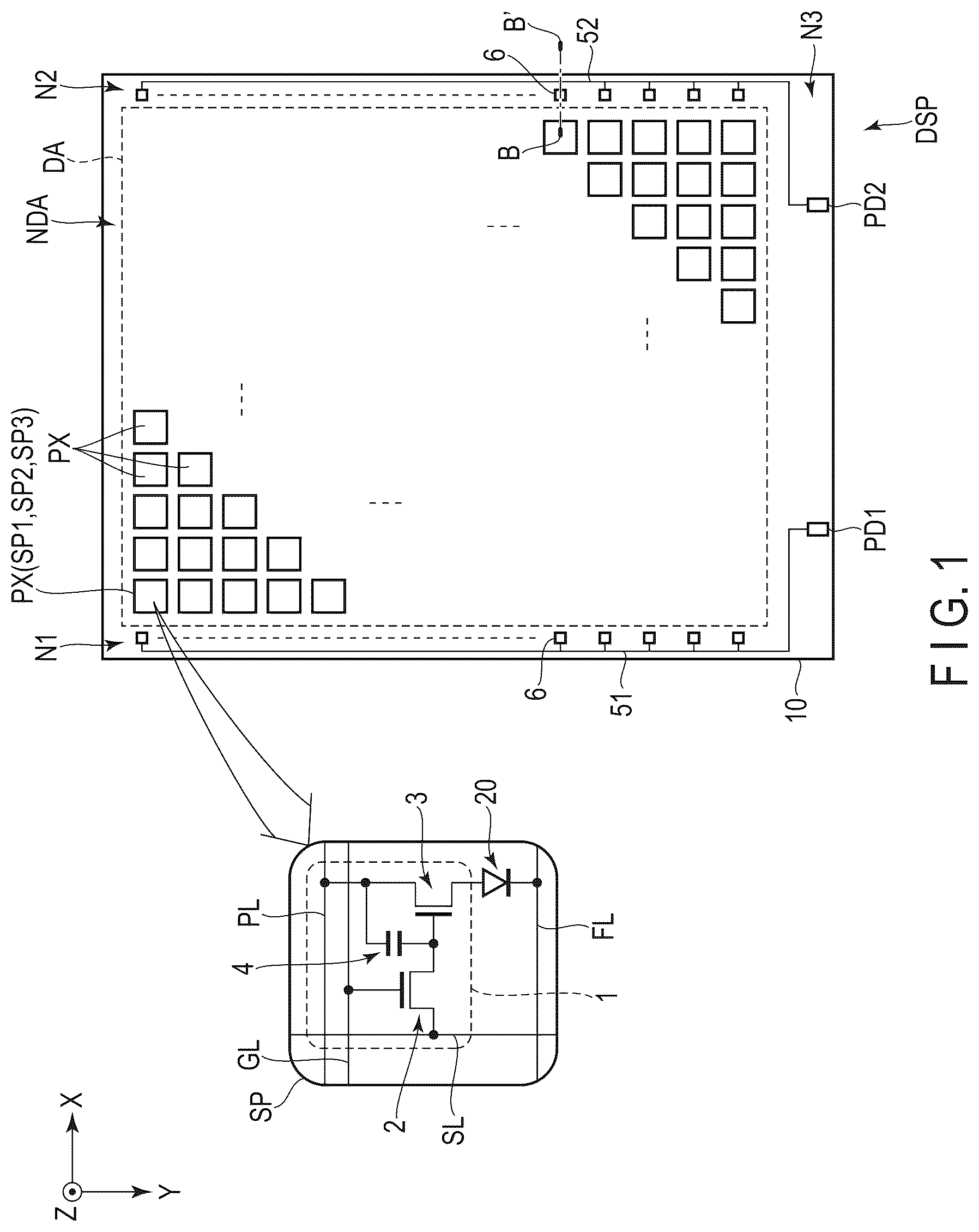
is a plan view showing a configuration example of a display device according to one embodiment.
is a plan view of a pixel.
is a cross-sectional view of the display device taken along line A-A′ shown in .
is a cross-sectional view showing a trench, an organic layer and the like.
is a plan view showing the organic layer.
is a cross-sectional view showing the display device taken along line B-B′ shown in .
is a cross-sectional view showing the first modified example of this embodiment.
is a plan view showing the second modified example of this embodiment.
is a plan view showing the third modified example of this embodiment.
DETAILED DESCRIPTION
In general, according to one embodiment, a display device comprises a base, a first insulating layer disposed on the base, a first lower electrode and a second lower electrode, disposed on the first insulating layer, a second insulating layer disposed on the first insulating layer and including a first opening overlapping the first lower electrode, a second opening overlapping the second lower electrode, and a first trench located between the first opening and the second opening, an organic layer including a light-emitting layer and an upper electrode covering the organic layer, and the first trench includes a bottom surface and first and second side surfaces rising from the bottom surface, an interval between the first side surface and the second side surface in an upper portion of the first trench is smaller than an interval between the first side surface and the second side surface in the bottom surface of the first trench, and the organic layer includes a first portion covering the first lower electrode located in the first opening and covering the first surface of the second insulating layer located between the first trench and the first opening, a second portion covering the second lower electrode located in the second opening and covering the second surface of the second insulating layer located between the first trench and the second opening and a third portion disposed on the bottom surface of the first trench and spaced apart from the first portion and the second portion.
Embodiments will be described hereinafter with reference to the accompanying drawings. The disclosure is merely an example, and proper changes within the spirit of the invention, which are easily conceivable by a skilled person, are included in the scope of the invention as a matter of course. In addition, in some cases, in order to make the description clearer, the widths, thicknesses, shapes, etc., of the respective parts are schematically illustrated in the drawings, compared to the actual modes. However, the schematic illustration is merely an example, and adds no restrictions to the interpretation of the invention. Besides, in the specification and drawings, the same elements as those described in connection with preceding drawings are denoted by like reference numerals, and a detailed description thereof is omitted unless otherwise necessary.
The display device DSP of this embodiment is an organic electroluminescent display device comprising an organic light-emitting diode (OLED) as a display element, and can be mounted on televisions, personal computers, mobile terminals, cell phones and the like.
is a plan view showing an example configuration of a display device DSP of this embodiment.
Some of the drawings illustrate a first direction X, a second direction Y and a third direction Z which are orthogonal to each other, but they may intersect at an angle other than 90 degrees. In the following descriptions, a direction forwarding a tip of an arrow indicating the third direction Z is referred to as “upward” and a direction forwarding oppositely from the tip of the arrow is referred to as “downward”. Further, it is assumed that there is an observation position to observe the semiconductor substrate on a tip side of an arrow in the third direction Z, and viewing from this observation position toward the X-Y plane defined by the first direction X and the second direction Y is referred to as a planar view.
The display device DSP comprises an insulating base 10 . The base 10 may be glass or a flexible resin film. The display device DSP includes a display area DA where images are displayed and a non-display area NDA around the display area DA.
The display device DSP comprises a plurality of pixels PX arranged in a matrix along the first direction X and the second direction Y in the display area DA. The pixels PX each comprises a plurality of subpixels SP 1 , SP 2 and SP 3 . For example, each pixel PX comprises a red subpixel SP 1 , a green subpixel SP 2 and a blue subpixel SP 3 . In place of the three subpixels of the three colors, the pixel PX may contain four or more subpixels of other colors, including white.
A configuration example of one subpixel SP contained in a pixel PX will be briefly described.
That is, the subpixel SP comprises a pixel circuit 1 and a display element 20 that is driven and controlled by the pixel circuit 1 . The pixel circuit 1 comprises a pixel switch 2 , a drive transistor 3 and a capacitor 4 . The pixel switch 2 and the drive transistor 3 are switch elements constituted by thin-film transistors, for example.
In the pixel switch 2 , a gate electrode thereof is connected to a scanning line GL, a source electrode is connected to a signal line SL and a drain electrode is connected to one of the electrodes constituting the capacitor 4 and the gate electrode of the drive transistor 3 . In the drive transistor 3 , a source electrode thereof is connected to the other electrode of the capacitor 4 and a power line PL, and a drain electrode is connected to an anode of the display element 20 . A cathode of the display element 20 is connected to a power feed line FL. Note that the configuration of the pixel circuit 1 is not limited to that of the example shown in the figure.
The display element 20 is an organic light-emitting diode (OLED), which is a light-emitting element. For example, a subpixel SP 1 comprises a display element that emits light corresponding to the red wavelength, a subpixel SP 2 comprises a display element that emits light corresponding to the green wavelength, and a subpixel SP 3 comprises a display element that emits light corresponding to the blue wavelength. The configuration of the display element 20 will be described later.
The display device DSP comprises power lines 51 and 52 located in the non-display area NDA, a plurality of peripheral electrodes 6 , and pads PD 1 and PD 2 . The non-display area NDA includes a first area N 1 and a second area N 2 , extending along the second direction Y, and a third area N 3 extending in the first direction X. The first area N 1 , the display area DA and the second area N 2 are aligned along the first direction X in this order. On the third area N 3 , a flexible wiring board (not shown) is mounted.
The power line 51 is located in the first area N 1 , and the power line 52 is located in the second area N 2 . The peripheral electrodes 6 are aligned along the second direction Y in each of the first and second regions N 1 and N 2 . The pads PD 1 and PD 2 are located in the third area N 3 .
The power line 51 is electrically connected to peripheral electrodes 6 located in the first area N 1 . The power line 51 is electrically connected to the pad PD 1 as well. The power line 52 is electrically connected to peripheral electrodes 6 located in the second area N 2 . The power line 52 is electrically connected to the pad PD 2 as well.
is a plan view showing a pixel PX.
illustrates lower electrodes E 11 , E 12 and E 13 of the display device DSP and the insulating layer 12 .
The lower electrode (first lower electrode) E 11 is located in the subpixel SP 1 . The lower electrode (second lower electrode) E 12 is located in the subpixel SP 2 . The lower electrode E 13 is placed in the subpixel SP 3 . The lower electrodes E 11 to E 13 are aligned along the first direction X. The lower electrodes, including the lower electrodes E 11 to E 13 , are electrodes each arranged for each respective subpixel or each respective display element, and may be referred to as pixel electrodes, anodes or the like.
The insulating layer 12 is formed into a grid pattern in planar view. The insulating layer 12 is formed in such a manner that it is partitioned into display elements or subpixels, and it may be referred to as ribs, partition walls, etc. The insulating layer 12 comprises a first opening OP 1 overlapping the lower electrode E 11 , a second opening OP 2 overlapping the lower electrode E 12 , and a third opening OP 3 overlapping the lower electrode E 13 . The insulating layer 12 covers the peripheral portion of each of the lower electrodes E 11 and E 13 , thus exposing a central portion of each of the lower electrodes E 11 to E 13 from the insulating layer 12 in the first opening OP 1 , the second opening OP 2 and the third opening OP 3 .
The insulating layer 12 comprises trenches T 11 , T 12 , T 13 and T 14 extending along the second direction Y and aligned along the first direction X, and trenches T 21 and T 22 extending along the first direction X and aligned along the second direction Y. The trench (first trench) T 12 is located between the first opening OP 1 and the second opening OP 2 . The trench T 13 is located between the second opening OP 2 and the third opening OP 3 . The trench T 11 is located on an opposite side to the trench T 12 while interposing the first opening OP 1 therebetween. The trench T 14 is located on an opposite side to the trench T 13 while interposing the third opening OP 3 . The trench T 21 is connected to the trenches T 11 to T 14 . The trench T 22 as well is connected to the trenches T 11 to T 14 . The trench T 21 is located on an opposite side to the trench T 22 while interposing the first opening OP 1 , the second opening OP 2 and the third opening OP 3 therebetween.
Each trench does not overlap a lower electrode adjacent thereto in plan view. The lower electrode E 11 is located between the trenches T 11 and T 12 , the lower electrode E 12 is located between the trenches T 12 and T 13 , and the lower electrode E 13 is located between the trenches T 13 and T 14 . The lower electrodes E 11 through E 13 are located between the trenches T 21 and T 22 .
Here, the outline of the subpixel corresponds to the outline of the lower electrode, for example. That is, the subpixels SP 1 , SP 2 and SP 3 , which constitute one pixel PX, are each formed in a substantially rectangular shape elongating along the second direction Y, and are aligned along the first direction X. The colors of the light emitted from adjacent subpixels aligned along the first direction X are different from each other. The areas of the subpixels SP 1 , SP 2 and SP 3 may be the same as or may be different from each other, as will be described below. The outline of each subpixel may be defined by the outline of the light-emitting area of the display element.
is a cross-sectional view of the display device DSP taken along line A-A′ shown in .
The display device DSP comprises a base 10 , switching elements SW 1 and SW 2 , an insulating layer 11 , lower electrodes E 11 and E 12 , an insulating layer 12 , an organic layer OR and an upper electrode E 2 . The display element 20 A is constituted by the lower electrode E 11 , a first portion OR 1 of the organic layer OR and the upper electrode E 2 . The display element 20 B is constituted by the lower electrode E 12 , a second portion OR 2 of the organic layer OR and the upper electrode E 2 .
The switching elements SW 1 and SW 2 are disposed on the base 10 . The switching elements SW 1 and SW 2 correspond, for example, to the drive transistor 3 shown in . The insulating layer (first insulating layer) 11 is disposed on the base 10 and covers the switching elements SW 1 and SW 2 . The insulating layer 11 corresponds to an underlying layer of the display elements 20 A and 20 B, and is, for example, an organic insulating layer. Note that the pixel switch 2 of the pixel circuit 1 and the like shown in are disposed on the base 10 and covered by the insulating layer 11 , but the illustration thereof is omitted here.
The lower electrodes E 11 and E 12 are disposed on the insulating layer 11 . The lower electrode E 11 is electrically connected to the switching element SW 1 via a contact hole CH 1 formed in the insulating layer 11 . The lower electrode E 12 is electrically connected to the switching element SW 2 via a contact hole CH 2 formed in the insulating layer 11 .
The lower electrodes E 11 and E 12 are transparent electrodes formed, for example, of a transparent conductive material such as indium tin oxide (ITO) or indium zinc oxide (IZO). The lower electrodes E 11 and E 12 may each be a metal electrode formed of a metal material such as silver or aluminum. Or, the lower electrodes E 11 and E 12 each may as well be a stacked body of a transparent electrode and a metal electrode. For example, the lower electrodes E 11 and E 12 may each be configured as a stacked body in which a transparent electrode, a metal electrode and a transparent electrode are stacked in this order, or may be configured as a stacked body consisting of three or more layers.
The insulating layer (second insulating layer) 12 is disposed on the insulating layer 11 and covers the peripheral portions of the lower electrodes E 11 and E 12 , respectively. The insulating layer 12 is, for example, an organic insulating layer. The insulating layer 12 comprises the first opening OP 1 , the second opening OP 2 and the trench T 12 , described above, and a first surface SF 1 and a second surface SF 2 . The first opening OP 1 penetrates the insulating layer 12 to the lower electrode E 11 . The second opening OP 2 penetrates the insulating layer 12 to the lower electrode E 12 . The first surface SF 1 is located between the trench T 12 and the first opening OP 1 . The second surface SF 2 is located between the trench T 12 and the second opening OP 2 . The insulating layer 12 has a thickness TH. The thickness TH corresponds to the distance between the highest position of the insulating layer 12 and the insulating layer 11 in the example illustrated in the figure, and is, for example, 1.5 to 2.0 μm.
The trench T 12 includes a bottom surface BS, and first and second side surfaces SS 1 and SS 2 rising from the bottom surface BS. The first and second side surfaces SS 1 and SS 2 oppose each other with an interval therebetween along the first direction X. The first side surface SS 1 is connected to the first surface SF 1 . The second side surface SS 2 is connected to the second surface SF 2 . The trench T 12 corresponds to the space surrounded by the first side surface SS 1 , the second side surface SS 2 and the bottom surface BS. The trench T 12 has a depth D. The depth D is, for example, 0.5 to 1.0 μm.
The trench T 12 comprises a gap GP 1 between the first side surface SS 1 and the second side surface SS 2 in its upper portion UP, and a gap GP 2 between the first side surface SS 1 and the second side surface SS 2 in its bottom surface BS. The gap GP 1 is less than the gap GP 2 . That is, the trench T 12 is formed such that the width along the first direction X decreases as its location is closer to the upper portion UP from the bottom surface BS. In other words, the first side surface SS 1 is inclined to the normal direction of the bottom surface BS so as to overlap the bottom surface BS. Similarly, the second side surface SS 2 is inclined in the normal direction to the bottom surface BS so as to overlap the bottom surface BS.
The organic layer OR includes a first portion OR 1 , a second portion OR 2 and a third portion OR 3 . The first portion OR 1 covers the lower electrode E 11 located in the first opening OP 1 and the first surface SF 1 . The second portion OR 2 covers the lower electrode E 12 located in the second opening OP 2 and the second surface SF 2 . The third portion OR 3 is located on the bottom surface BS of the trench T 12 . The third portion OR 3 is separated from the first portion OR 1 and the second portion OR 2 . The organic layer OR includes a light-emitting layer EL as described below, and the first portion OR 1 , the second portion OR 2 and the third portion OR 3 include light-emitting layers EL of the same color. Further, the organic layer OR includes, in addition to the light-emitting layer EL, at least one of a hole injection layer, a hole transport layer, an electron injection layer, and an electron transport layer.
The upper electrode E 2 covers the organic layer OR. That is, the upper electrode E 2 covers each of the first portion OR 1 , the second portion OR 2 and the third portion OR 3 . The upper electrode E 2 covers the third portion OR 3 inside the trench T 12 and is in contact with the bottom surface BS. Further, the upper electrode E 2 is also in contact with the first side surface SS 1 and the second side surface SS 2 inside the trench T 12 . The upper electrode E 2 is a transparent electrode formed of a transparent conductive material such as ITO or IZO. The upper electrode E 2 is electrically connected to the power feed line FL located in the display area DA shown in . The upper electrode E 2 is an electrode commonly provided for multiple subpixels or multiple display elements, and may be referred to as a common electrode, counter electrode, cathode or the like. The upper electrode E 2 may be covered by a transparent protective layer (including at least one of an inorganic insulating layer and an organic insulating layer).
In the display element 20 A, the first portion OR 1 is located between the lower electrode E 11 and the upper electrode E 2 and thus can form a light-emitting region. In the display device 20 B, the second portion OR 2 is located between the lower electrode E 12 and the upper electrode E 2 , and thus can form a light-emitting region. The third portion OR 3 is located between the insulating layer 12 and the upper electrode E 2 , and is completely separated from the first portion OR 1 and the second portion OR 2 ; therefore it does not emit light. Further, of the first portion OR 1 , the region that covers the first surface SF 1 emits substantially no light because it is located between the insulating layer 12 and the upper electrode E 2 . Similarly, of the second portion OR 2 , the region that covers the second surface SF 2 emits substantially no light because it is located between the insulating layer 12 and the upper electrode E 2 .
The organic layer OR described above is formed, for example, by the vacuum deposition method. The figure illustrates by single-dotted chain lines, how the organic material to form the organic layer OR is ejected from the deposition source.
After forming the insulating layer 12 provided with the first opening OP 1 , the second opening OP 2 and the trench T 12 , the organic material to form the organic layer OR is deposited. Since the first side surface SS 1 is inclined so as to overlap the bottom surface BS, the organic layer OR is not substantially formed on the first side surface SS 1 . Thus, the organic layer OR is formed such that the first portion OR 1 and the third portion OR 3 are separated from each other. Similarly, since the second side surface SS 2 is inclined to overlap the bottom surface BS, substantially no organic layer OR is formed on the second side surface SS 2 . Thus, the organic layer OR is formed such that the second portion OR 2 and the third portion OR 3 are separated from each other. Further, in the region of the bottom surface BS that overlaps the first side surface SS 1 and the second side surface SS 2 along the third direction Z, substantially no organic layer OR is formed. Note that the upper electrode E 2 is formed by sputtering, and therefore it is continuously formed on the organic layer OR, the bottom surface BS, the first side surface SS 1 and the second side surface SS 2 .
According to this embodiment, the insulating layer 12 includes the trench T 12 . Further, the trench T 12 is formed such that the width along the first direction X decreases as the location closer to the upper portion UP from the bottom surface BS. With this structure, the organic layer OR can be formed in the trench T 12 such that the first portion OR 1 located in the subpixel SP 1 and the second portion OR 2 located in the subpixel SP 2 are separated from each other. In other words, the organic layer OR can be formed separately for each subpixel by an entire surface deposition without using a mask. Thus, it is possible to suppress crosstalk between adjacent subpixels. Further, separate members for separating the organic layers OR from each other are not necessary, and therefore the manufacturing cost can be reduced.
Note that the interval between the first side surface SS 1 and the second side surface SS 2 can be rephrased as the width of the trench T 12 . In the example illustrated in , the first side surface SS 1 , the second side surface SS 2 , and the bottom surface BS are flat surfaces, but they may as well be curved surfaces. When the first side surface SS 1 , the second side surface SS 2 , and the bottom surface BS are flat, the maximum width of the trench T 12 is equivalent to the width of the bottom surface BS. But, when the first side surface SS 1 , the second side surface SS 2 , and the bottom surface BS include curved surfaces, the maximum width of the trench T 12 does not necessarily correspond to the width of the bottom surface BS, and the width of the trench T 12 may be maximum above the bottom surface BS. In this case, for example, the width of the trench T 12 becomes maximum at a position of ½ or less or even ⅓ or less of the height of the trench T 12 .
When the potentials of the lower electrodes E 11 and E 12 are relatively higher than that of the upper electrode E 2 , the lower electrodes E 11 and E 12 correspond to the anodes and the upper electrode E 2 corresponds to the cathode. When the potential of the upper electrode E 2 is relatively higher than those of the lower electrodes E 11 and E 12 , the upper electrode E 2 corresponds to the anode and the lower electrodes E 11 and E 12 correspond to the cathode.
For example, in all subpixels SP in the display area DA, an organic layer OR including light-emitting layers EL of the same color is disposed. When the light-emitting color of the display elements is white, a multi-color display can be realized by disposing a color filter to oppose the display elements. When the light-emitting color of each display element is ultraviolet light, a multi-color display can be realized by disposing a photo-conversion layer to oppose the display elements.
is a cross-sectional view showing the trench T 12 , the organic layer OR, etc.
The organic layer OR includes a first layer L 1 , a second layer L 2 and a third layer L 3 , stacked on one another. That is, the first portion OR 1 , the second portion OR 2 and the third portion OR 3 includes the first layer L 1 , the second layer L 2 and the third layer L 3 , stacked one on another, respectively. As described above, the organic layer OR includes the light-emitting layer EL. For example, the light-emitting layer EL is any one of the first layer L 1 , the second layer L 2 and the third layer L 3 .
The first portion OR 1 is in contact with the first side surface SS 1 . In the first side surface SS 1 , an edge portion EG 11 of the first layer L 1 is covered by the second layer L 2 , and an edge portion EG 21 of the second layer L 2 is covered by the third layer L 3 . The second portion OR 2 is in contact with the second side surface SS 2 . In the second side surface SS 2 , an edge portion EG 12 of the first layer L 1 is covered by the second layer L 2 , and an edge portion EG 22 of the second layer L 2 is covered by the third layer L 3 .
In this embodiment, the first side surface SS 1 and the second side surface SS 2 are each inclined to overlap with the bottom surface BS, and therefore the second layer L 2 is deposited to cover the first layer L 1 and the third layer L 3 is deposited to cover the second layer L 2 . With this configuration, it is possible to suppress the first layer L 1 and the second layer L 2 from being exposed from the third layer L 3 , and the upper electrode E 2 can be suppressed from coming into contact with the first layer L 1 and the second layer L 2 . Therefore, the leakage of current from the first and second layers L 1 and L 2 to the upper electrode E 2 is suppressed, thus making it possible to suppress the degradation performance of the display element.
Here, let us suppose, for example, that the first layer L 1 and the third layer L 3 are functional layers and the second layer L 2 is a light-emitting layer EL. The first layer L 1 and the third layer L 3 are, for example, a hole injection layer, a hole transport layer, a hole blocking layer, an electron injection layer, an electron transport layer, and an electron blocking layer, but they may as well be other functional layers. Each of the first layer L 1 and the third layer L 3 is not limited to a single layer, but may as well be a stacked body in which multiple functional layers are stacked. Further, at least one of the first layer L 1 and the third layer L 3 may be omitted.
For example, when the lower electrode corresponds to an anode, the first layer L 1 between the light-emitting layer EL and the lower electrode includes at least one of a hole injection layer and a hole transport layer, and the third layer L 3 between the light-emitting layer EL and the upper electrode E 2 includes at least one of an electron transport layer and an electron injection layer.
is a plan view of the organic layer OR. In , the region where the organic layer OR is disposed is indicated by shaded lines.
The first portion OR 1 is disposed in the subpixel SP 1 . The second portion OR 2 is disposed in the subpixel SP 2 . The first portion OR 1 and the second portion OR 2 are aligned along the first direction X.
The third portion OR 3 is formed into a grid pattern in planar view. The third portion OR 3 includes parts OR 31 , OR 32 and OR 33 extending along the second direction Y and aligned along the first direction X, and parts OR 34 and OR 35 extending along the first direction X and aligned along the second direction Y. The part OR 32 is located between the first portion OR 1 and the second portion OR 2 . The part OR 31 is located on an opposite side to the part OR 32 while interposing the first portion OR 1 therebetween. The part OR 33 is located on an opposite side to the part OR 32 while interposing the second portion OR 2 . The part OR 34 is connected to the portions OR 31 and OR 33 . The part OR 35 is connected to the portions OR 31 and OR 33 . The part OR 34 is located on an opposite side to the part OR 35 while interposing the first portion OR 1 and the second portion OR 2 therebetween.
The parts OR 31 to OR 33 are located in the trenches T 11 to T 13 , respectively. Further, the parts OR 34 and OR 35 are located in the trenches T 21 and T 22 , respectively.
Note that the outer shape of the first portion OR 1 is greater in size than that of the lower electrode E 11 in planar view. The outer shape of the second portion OR 2 is greater in size than that of the lower electrode E 12 in planar view.
is a cross-sectional view of the display device DSP taken along line B-B′ shown in .
The peripheral electrode 6 and the power line 52 are located on the insulating layer 11 . The insulating layer 12 covers the peripheral electrode 6 and power lines 52 . The organic layer OR is not formed in the non-display area NDA. The upper electrode E 2 covers the insulating layer 12 in the non-display area NDA and is connected to the peripheral electrodes 6 via a contact hole CH 3 formed in the insulating layer 12 . In the example illustrated in the figure, the peripheral electrode 6 and the power line 52 are located in the same layer as that of the lower electrode E 10 , but each may be located on a different layer from that of the lower electrode E 10 .
is a cross-sectional view of the first modified example of the embodiment. The configuration shown in is different from that of in that the trench T 12 penetrates the insulating layer 12 to the insulating layer 11 .
In the example illustrated in the figure, the bottom surface BS corresponds to the upper surface of the insulating layer 11 . Therefore, the third portion OR 3 and the upper electrode E 2 are in contact with the insulating layer 11 in the trench T 12 .
In the first modified example with such a configuration as described above, effects similar to those described above can be obtained.
is a plan view of the second modified example of the embodiment. The configuration shown in is different from that of in the layout of the subpixel SP 1 , subpixel SP 2 and subpixel SP 3 .
The lower electrodes E 11 and E 12 are aligned along the second direction Y. The lower electrodes E 13 is aligned with the lower electrodes E 11 and E 12 along the first direction X.
The insulating layer 12 includes trenches T 15 , T 16 and T 17 extending in the second direction Y and aligned in the first direction X, and trenches T 23 , T 24 and T 25 extending in the first direction X and aligned in the second direction Y. The trench T 16 is located between the first and second openings OP 1 and OP 2 , and the third opening OP 3 . The trench T 15 is located on an opposite side to the trench T 16 while interposing the first and second openings OP 1 and OP 2 therebetween. The trench T 17 is located on an opposite side to the trench T 16 while interposing the third opening OP 3 therebetween. The trench T 23 is connected to the trenches T 15 to T 17 . The trench T 24 is connected to the trenches T 15 and T 16 . The trench T 25 is connected to the trenches T 15 to T 17 . The trench T 23 is located on an opposite side to the trench T 25 while interposing the first opening OP 1 , the second opening OP 2 and the third opening OP 3 therebetween. The trench T 24 is located between the first opening OP 1 and the second opening OP 2 .
Each trench does not overlap a respective lower electrode adjacent thereto in planar view. In the first direction X, the lower electrodes E 11 and E 12 are located between the trenches T 15 and T 16 , and the lower electrode E 13 is located between the trenches T 16 and T 17 . In the second direction Y, the lower electrode E 11 is located between the trenches T 23 and T 24 , the lower electrode E 12 is located between the trenches T 24 and T 25 , and the lower electrode E 13 is located between the trenches T 23 and T 25 .
The subpixels SP 1 and SP 2 are aligned along the second direction Y. The subpixels SP 1 and SP 3 are aligned along the first direction X. The subpixels SP 2 and SP 3 are aligned in the first direction X. The subpixel SP 1 is formed into a rectangular shape elongated along the first direction X, and the subpixels SP 2 and SP 3 are each formed into a rectangular shape elongated along the second direction Y. The colors of light emitted from the subpixels SP 1 and SP 3 are different from each other. Further, the areas of the subpixels SP 1 to SP 3 are different from each other. The area of the subpixel SP 2 is greater than that of the subpixel SP 1 , and the area of the subpixel SP 3 is greater than that of the subpixel SP 2 . The area of the subpixel SP 1 may be the same as that of the subpixel SP 2 .
In the second modified example with such a configuration as described above, effects similar to those described above can be obtained.
is a plan view of the third modified example of the embodiment. The configuration shown in is different from that of in the layout of the subpixel SP 1 , subpixel SP 2 and subpixel SP 3 . A direction DR 1 shown in is inclined counterclockwise to the second direction Y at an angle θ 1 , and a direction DR 2 shown in is inclined clockwise to the second direction Y at an angle θ 2 .
The insulating layer 12 includes a plurality of trenches T 1 extending along the direction DR 1 and aligned along the direction DR 2 , and a plurality of trenches T 2 extending along the direction DR 2 and aligned along the direction DR 1 . A plurality of lower electrodes E 11 and a plurality of first openings OP 1 are located in a plurality of red subpixels SP 1 , respectively. A plurality of lower electrodes E 12 and a plurality of second openings OP 2 are located in a plurality of green subpixels SP 2 , respectively. A plurality of lower electrodes E 13 and a plurality of third openings OP 3 are located in a plurality of blue subpixels SP 3 , respectively.
The lower electrodes E 11 and E 12 are alternately arranged along the direction DR 1 between each adjacent pair of trenches T 1 . The lower electrodes E 12 and E 13 are alternately arranged along the direction DR 1 between each adjacent pair of trenches T 1 . The lower electrodes E 11 and E 12 are alternately arranged along the direction DR 2 between each adjacent pair of trenches T 2 . The lower electrodes E 12 and E 13 are alternately arranged along the direction DR 2 between each adjacent pair of trenches T 2 . Each of the trenches T 1 and T 2 does not overlap the lower electrode adjacent thereto in planar view.
The subpixels SP 1 and SP 3 are formed into a substantially square shape, some of the subpixels SP 2 are formed into a substantially rectangular shape elongated along the direction DR 1 , and other subpixels SP 2 are formed into a substantially rectangular shape elongated along the direction DR 2 . The areas of the subpixels SP 1 to SP 3 are different from each other. The area of the subpixels SP 3 is greater than that of the subpixels SP 1 , and the area of the subpixels SP 1 is greater than that of the subpixels SP 2 .
In the third modified example with such a configuration as described above, effects similar to those described above can be obtained.
As explained above, according to the present embodiments, it is possible to provide a display device which can suppress the degradation of display quality.
While certain embodiments have been described, these embodiments have been presented by way of example only, and are not intended to limit the scope of the inventions. Indeed, the novel embodiments described herein may be embodied in a variety of other forms; furthermore, various omissions, substitutions and changes in the form of the embodiments described herein may be made without departing from the spirit of the inventions. The accompanying claims and their equivalents are intended to cover such forms or modifications as would fall within the scope and spirit of the inventions.
Figures (9)
Citations
This patent cites (15)
- US12035571
- US2015/0179718
- US2015/0279915
- US2016/0240598
- US2017/0207285
- US2017/0250367
- US2017/0271421
- US2018/0301521
- US2019/0172898
- US2019/0198590
- US2020/0098983
- US106876331
- US2008135325
- US2009244527
- US2017174811