Abstract
A semiconductor device includes a first device including first active regions and first to third structures thereon, and a second device including a second active region, a gate structure intersecting the second active region, and a source/drain region including a lower source/drain region on the second active region having first-type conductivity, an inter-source/drain region insulating layer on the lower source/drain region, and an upper source/drain region on the inter-source/drain region insulating layer and having second-type conductivity. The first structure includes first lower and upper impurity regions. The second structure includes a second lower impurity region having the first-type conductivity, an inter-impurity region insulating layer, and a second upper impurity region having the second-type conductivity. The third structure includes third lower and upper impurity regions having the second-type conductivity, the third upper impurity region having an impurity concentration higher than a that of the third lower impurity region.
Claims (20)
1. A semiconductor device, comprising: a first device including first active regions spaced apart from each other on a substrate, and a first structure, a second structure, and a third structure on each of the first active regions; and a second device including a second active region spaced apart from the first active regions on the substrate and extending in a first direction parallel to an upper surface of the substrate, at least one gate structure intersecting the second active region and extending in a second direction, a source/drain region including a lower source/drain region on the second active region on at least one side of the gate structure and having first-type conductivity, an inter-source/drain region insulating layer on the lower source/drain region, and an upper source/drain region on the inter-source/drain region insulating layer and having second-type conductivity different from the first-type conductivity, wherein: the first structure includes a first lower impurity region and a first upper impurity region on the first lower impurity region, the second structure includes a second lower impurity region having the first-type conductivity, an inter-impurity region insulating layer on the second lower impurity region, and a second upper impurity region on the inter-impurity region insulating layer and having the second-type conductivity, and the third structure includes a third lower impurity region having the second-type conductivity and a third upper impurity region on the third lower impurity region having the second-type conductivity and having an impurity concentration higher than an impurity concentration of the third lower impurity region.
13. A semiconductor device, comprising: a first device including a first structure, a second structure, and a third structure spaced apart from each other on a substrate; a second device including an active region extending in a first direction parallel to an upper surface of the substrate, at least one gate structure intersecting the active region and extending in a second direction, a source/drain region including a lower source/drain region on the active region on at least one side of the gate structure and having first-type conductivity, an inter-source/drain region insulating layer on the lower source/drain region, and an upper source/drain region on the inter-source/drain region insulating layer and having second-type conductivity different from the first-type conductivity, wherein: the first structure includes a first lower impurity region having the second-type conductivity, and a first upper impurity region on the first lower impurity region having the second-type conductivity and having an impurity concentration higher than an impurity concentration of the first lower impurity region, the second structure includes a second lower impurity region having the first-type conductivity, an inter-impurity region insulating layer on the second lower impurity region, and a second upper impurity region on the inter-impurity region insulating layer and having the second-type conductivity, and the third structure includes a third lower impurity region having the second-type conductivity, and a third upper impurity region on the third lower impurity region and having the second-type conductivity.
16. A semiconductor device, comprising: a first device including a first structure, a second structure, and a third structure spaced apart from each other on a substrate; a second device including an active region extending in a first direction parallel to an upper surface of the substrate, at least one gate structure intersecting the active region and extending in a second direction, a source/drain region including a lower source/drain region on the active region on at least one side of the gate structure and having first-type conductivity, an inter-source/drain region insulating layer on the lower source/drain region, and an upper source/drain region on the inter-source/drain region insulating layer and having second-type conductivity different from the first-type conductivity, wherein: the first structure includes a first lower impurity region having the first-type conductivity, and a first upper impurity region on the first lower impurity region and having the first-type conductivity, the second structure includes a second lower impurity region having a stack structure of first and second semiconductor layers alternately stacked and having the second-type conductivity, and a second upper impurity region including a third semiconductor layer on the second lower impurity region and having the second-type conductivity, the first semiconductor layers are first material layers, the second semiconductor layers are second material layers different from the first material layers, the third semiconductor layer is a third material layer different from at least one of the first and second material layers, a thickness of the third material layer is greater than a thickness of each of the first and second material layers, and the third structure includes a third lower impurity region having the first-type conductivity, an inter-impurity region insulating layer on the third lower impurity region, and a third upper impurity region on the inter-impurity region insulating layer and having the second-type conductivity.
Show 17 dependent claims
2. The semiconductor device as claimed in claim 1 , wherein: the impurity concentration of the third lower impurity region is in a range of about 1×10 19 /cm 3 to 5×10 19 /cm 3 , and the impurity concentration of the third upper impurity region is in a range of about 1×10 20 /cm 3 to 5×10 20 /cm 3 .
3. The semiconductor device as claimed in claim 1 , wherein the inter-impurity region insulating layer electrically separates the second lower impurity region from the second upper impurity region.
4. The semiconductor device as claimed in claim 1 , wherein: the second lower impurity region is spaced apart from the second upper impurity region, and the third lower impurity region is in contact with the third upper impurity region.
5. The semiconductor device as claimed in claim 1 , wherein the inter-impurity region insulating layer includes a same material as a material of the inter-source/drain region insulating layer.
6. The semiconductor device as claimed in claim 1 , wherein: each of the first lower impurity region and the first upper impurity region has the second-type conductivity, the first lower impurity region includes a stack structure of first semiconductor layers and second semiconductor layers alternately stacked, the first semiconductor layers are first material layers, the second semiconductor layers are second material layers different from the first material layers, the first upper impurity region includes a third semiconductor layer configured as a third material layer, the third material layer is different from at least one of the first and second material layers, and a thickness of the third material layer is greater than a thickness of each of the first and second material layers.
7. The semiconductor device as claimed in claim 1 , wherein: an impurity concentration of the first lower impurity region is lower than an impurity concentration of the first upper impurity region, and the first lower impurity region is on substantially the same level as a level of the lower source/drain region.
8. The semiconductor device as claimed in claim 1 , wherein: the third lower impurity region includes a stack structure of first semiconductor layers and second semiconductor layers alternately stacked, the third upper impurity region includes a third semiconductor layer, the third semiconductor layer includes a material different from a material of at least one of the first semiconductor layers and the second semiconductor layers, and a thickness of the third semiconductor layer is greater than a thickness of each of the first and second semiconductor layers.
9. The semiconductor device as claimed in claim 1 , further comprising: an emitter contact plug in contact with the first upper impurity region; a base contact plug in contact with the second lower impurity region; and a collector contact plug in contact with the third upper impurity region.
10. The semiconductor device as claimed in claim 9 , wherein: the base contact plug includes a plug layer and a sidewall insulating layer covering a side surface of the plug layer, the plug layer is spaced apart from the second upper impurity region, and the base contact plug penetrates the second upper impurity region, and is in contact with the second lower impurity region.
11. The semiconductor device as claimed in claim 9 , wherein the base contact plug includes: a horizontal contact plug connected to at least a portion of a side surface of the second lower impurity region; and a vertical contact plug not in contact with the second upper impurity region, and connected to the horizontal contact plug.
12. The semiconductor device as claimed in claim 1 , further comprising dummy gate structures on upper surfaces of each of the second and third structures, respectively, the dummy gate structures extending and being spaced apart from the gate structure, wherein the dummy gate structures are not on the first structure.
14. The semiconductor device as claimed in claim 13 , further comprising: an emitter contact plug in contact with at least one of the first upper and lower impurity regions; a base contact plug in contact with the second lower impurity region; and a collector contact plug in contact with at least one of the third upper and lower impurity regions.
15. The semiconductor device as claimed in claim 13 , wherein: the second device includes a plurality of channel layers spaced apart from each other in a direction perpendicular to the upper surface of the substrate on the active region, and in contact with the source/drain region on at least one side, and the second structure includes dummy channel layers on the same level as a level of the plurality of channel layers, and in contact with at least one side of the second lower impurity region, the inter-impurity region insulating layer, and the second upper impurity region.
17. The semiconductor device as claimed in claim 16 , further comprising: an emitter contact plug in contact with at least one of the first upper and lower impurity regions; a base contact plug in contact with at least one of the second upper and lower impurity regions; and a collector contact plug in contact with the third lower impurity region.
18. The semiconductor device as claimed in claim 16 , wherein an impurity concentration of the first upper impurity region is higher than an impurity concentration of the first lower impurity region.
19. The semiconductor device as claimed in claim 16 , wherein an impurity concentration of the second lower impurity region is lower than an impurity concentration of the second upper impurity region.
20. The semiconductor device as claimed in claim 16 , wherein: the third lower impurity region is electrically isolated from the third upper impurity region, and the second lower impurity region is electrically connected to the second upper impurity region.
Full Description
Show full text →
CROSS TO REFERENCE TO RELATED APPLICATION
This application claims benefit of priority to Korean Patent Application No. 10-2021-0119626 filed on Sep. 8, 2021, in the Korean Intellectual Property Office, the disclosure of which is incorporated herein by reference in its entirety.
BACKGROUND
1. Field
Embodiments relate to a semiconductor device.
2. Description of the Related Art
As demand for high performance, high speed, and/or multifunctionality of semiconductor devices has increased, integration density of a semiconductor device has increased. In manufacturing a semiconductor device having a fine pattern for high integration density of a semiconductor device, it may be important to implement patterns having a fine width or a fine spacing. Also, to address changes in operating properties due to a reduced size of a planar metal oxide semiconductor FET (MOSFET), a semiconductor device including a FinFET having a three-dimensional channel structure may be considered.
SUMMARY
According to an embodiment, a semiconductor device includes a first device including first active regions spaced apart from each other on a substrate, and a first structure, a second structure, and a third structure on each of the first active regions, and a second device including a second active region spaced apart from the first active regions on the substrate and extending in a first direction parallel to an upper surface of the substrate, at least one gate structure intersecting the second active region and extending in a second direction, and a source/drain region including a lower source/drain region on the second active region on at least one side of the gate structure and having first-type conductivity, an inter-source/drain region insulating layer on the lower source/drain region, and an upper source/drain region on the inter-source/drain region insulating layer having second-type conductivity different from the first-type conductivity, wherein the first structure includes a first lower impurity region and a first upper impurity region on the first lower impurity region, wherein the second structure includes a second lower impurity region having the first-type conductivity, an inter-impurity region insulating layer on the second lower impurity region, and a second upper impurity region on the inter-impurity region insulating layer and having the second-type conductivity, and wherein the third structure includes a third lower impurity region having the second-type conductivity and a third upper impurity region on the third lower impurity region having the second-type conductivity and having an impurity concentration higher than an impurity concentration of the third lower impurity region.
According to an embodiment, a semiconductor device includes a first device including a first structure, a second structure, and a third structure spaced apart from each other on a substrate, a second device including an active region extending in a first direction parallel to an upper surface of the substrate, at least one gate structure intersecting the active region and extending in a second direction, and a source/drain region including a lower source/drain region on the active region on at least one side of the gate structure and having first-type conductivity, an inter-source/drain region insulating layer on the lower source/drain region, and an upper source/drain region on the inter-source/drain region insulating layer having second-type conductivity different from the first-type conductivity, wherein the first structure includes a first lower impurity region having the second-type conductivity and a first upper impurity region on the first lower impurity region having the second-type conductivity and having an impurity concentration higher than an impurity concentration of the first lower impurity region, wherein the second structure includes a second lower impurity region having the first-type conductivity, an inter-impurity region insulating layer on the second lower impurity region, and a second upper impurity region on the inter-impurity region insulating layer and having the second-type conductivity, and wherein the third structure includes a third lower impurity region having the second-type conductivity and a third upper impurity region on the third lower impurity region and having the second-type conductivity.
According to an embodiment, a semiconductor device includes a first device including a first structure, a second structure, and a third structure spaced apart from each other on a substrate, a second device including an active region extending in a first direction parallel to an upper surface of the substrate, at least one gate structure intersecting the active region and extending in a second direction, a source/drain region including a lower source/drain region on the active region on at least one side of the gate structure and having first-type conductivity, an inter-source/drain region insulating layer on the lower source/drain region, and an upper source/drain region on the inter-source/drain region insulating layer and having second-type conductivity different from the first-type conductivity, wherein the first structure includes a first lower impurity region having the first-type conductivity and a first upper impurity region on the first lower impurity region and having the first-type conductivity, wherein the second structure includes a second lower impurity region having a stack structure of first and second semiconductor layers alternately stacked and having the second-type conductivity, and a second upper impurity region including a third semiconductor layer on the second lower impurity region and having the second-type conductivity, wherein the first semiconductor layers are first material layers, wherein the second semiconductor layers are second material layers different from the first material layers, wherein the third semiconductor layer is a third material layer different from at least one of the first and second material layers, wherein a thickness of the third material layer is greater than a thickness of each of the first and second material layers, and wherein the third structure includes a third lower impurity region having the first-type conductivity, an inter-impurity region insulating layer on the third lower impurity region, and a third upper impurity region on the inter-impurity region insulating layer and having the second-type conductivity.
BRIEF DESCRIPTION OF DRAWINGS
Features will become apparent to those of skill in the art by describing in detail example embodiments with reference to the attached drawings in which:
A and 1 B are plan diagrams illustrating a semiconductor device according to an example embodiment;
to 3 E are cross-sectional diagrams illustrating a semiconductor device according to an example embodiment;
is a cross-sectional diagram illustrating a semiconductor device according to an example embodiment;
is a cross-sectional diagram illustrating a semiconductor device according to an example embodiment; p is a cross-sectional diagram illustrating a semiconductor device according to an example embodiment;
is a cross-sectional diagram illustrating a semiconductor device according to an example embodiment;
is a cross-sectional diagram illustrating a semiconductor device according to an example embodiment;
A and 9 B are cross-sectional diagrams illustrating a semiconductor device according to an example embodiment;
is a cross-sectional diagram illustrating a semiconductor device according to an example embodiment;
A and 11 B are cross-sectional diagrams illustrating a semiconductor device according to an example embodiment;
A and 12 B are cross-sectional diagrams illustrating a semiconductor device according to an example embodiment;
A to 13 J are diagrams illustrating processes of a method of manufacturing a semiconductor device in order according to an example embodiment; and
A to 14 H are diagrams illustrating processes of a method of manufacturing a semiconductor device in order according to an example embodiment.
DETAILED DESCRIPTION
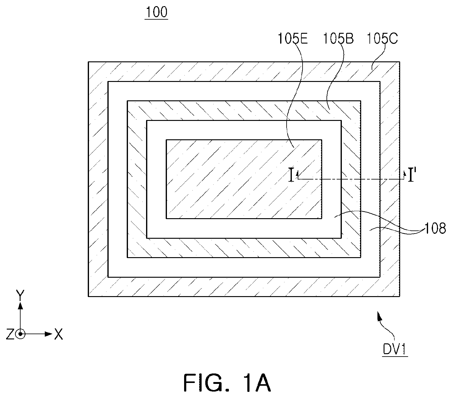
A and 1 B are plan diagrams illustrating a semiconductor device 100 according to an example embodiment. to 3 E are cross-sectional diagrams illustrating a semiconductor device 100 according to an example embodiment. is a cross-sectional diagram illustrating a semiconductor device 100 in A taken along I-I′, A is a cross-sectional diagram illustrating a semiconductor device 100 in B taken along 3 B is a cross-sectional diagram illustrating a semiconductor device 100 in B taken along line C is a cross-sectional diagram illustrating a semiconductor device 100 in B taken along line IV-IV′, D is a cross-sectional diagram illustrating a semiconductor device 100 in B taken along line V-V′, and E is a cross-sectional diagram illustrating a semiconductor device 100 in B taken along line VI-VI′. For ease of description, only main components of the semiconductor device are illustrated in A to 3 E .
Referring to A to 3 E , the semiconductor device 100 may include a first device DV 1 and a second device DV 2 spaced apart from the first device DV 1 .
Referring to A and 2 , the first device DV 1 may include a substrate 101 , first active regions 105 E, 105 B, and 105 C on the substrate 101 , isolation insulating layers 108 , a first structure E, a second structure B, a third structure C, first contact plugs 170 E, 170 B, and 170 C, and an interlayer insulating layer 190 . The first structure E, the second structure B, and the third structure C may be spaced apart from each other. The first structure E may include a first lower impurity region 151 E and a first upper impurity region 152 E. The second structure B may include a second lower impurity region 151 B, a second upper impurity region 152 B, and an inter-impurity region insulating layer 153 B. The third structure C may include a third lower impurity region 151 C and a third upper impurity region 152 C.
The first device DV 1 may be configured as a bipolar junction transistor (BJT) including the first structure E working as an emitter, the second structure B working as a base, and the third structure C working as a collector. The first device DV 1 may be a PNP device or an NPN device. The example embodiments may be described with reference to a PNP device, but the example embodiments may be implemented in an NPN device.
Referring to B and 3 A to 3 E , the second device DV 2 may include the substrate 101 , second active regions 105 T on the substrate 101 , device isolation layers 107 isolating the second active regions 105 T, channel layers 140 T on the second active regions 105 T, source/drain regions 150 T in contact with the channel layers 140 T, gate structures 160 T extending to intersect the second active regions 105 T, second contact plugs 170 T, and an interlayer insulating layer 190 . Each of the source/drain regions 150 T may include a lower source/drain region 151 T, an upper source/drain region 152 T, and an inter-source/drain region insulating layer 153 T. Each of the gate structures 160 T may include a gate dielectric layer 162 , a gate electrode 165 , a spacer structure 164 , and a capping layer 166 .
In the second device DV 2 , the second active regions 105 T may have a fin structure, and the gate electrode 165 may be disposed between the second active regions 105 T and the channel layers 140 T, between the channel layers 140 T, and on the uppermost surface of channel layers 140 T. Thus, the second device DV 2 of the semiconductor device 100 may include a gate-all-around type field effect transistor using the channel layers 140 T, the source/drain regions 150 T, and the gate structures 160 T.
The substrate 101 may have an upper surface extending in the X-direction and the Y-direction. The substrate 101 may include a semiconductor material, e.g., a group IV semiconductor, a group III-V compound semiconductor, or a group II-VI compound semiconductor. For example, the group IV semiconductor may include silicon, germanium, or silicon-germanium. The substrate 101 may be provided as a bulk wafer, an epitaxial layer, an epitaxial layer, a silicon on insulator (SOI) layer, or a semiconductor on insulator (SeOI) layer.
The first active regions 105 E, 105 B, and 105 C may respectively correspond to an emitter active region 105 E, a base active region 105 B, and a collector active region 105 C. The first active regions 105 E, 105 B, and 105 C may protrude from the upper surface of the substrate 101 in the vertical Z-direction. The first active regions 105 E, 105 B, and 105 C may be formed as a portion of the substrate 101 . The first active regions 105 E, 105 B, and 105 C may include a doped region. A lower emitter active region 105 E 1 of the emitter active region 105 E may be doped to have a first-type conductivity. An upper emitter active region 105 E 2 of the emitter active region 105 E may be doped to have a second-type conductivity, different from the first-type conductivity. The base active region 105 B may be doped to have the first-type conductivity. The collector active region 105 C may be doped to have the second-type conductivity. For example, the upper emitter active region 105 E 2 of the emitter active region 105 E and the collector active region 105 C may have P-type conductivity, and the lower emitter active region 105 E 1 of the emitter active region 105 E and the base active region 105 B may have N-type conductivity. In another implementation, the elements may be doped with a combination of different types of conductivity. The first active regions 105 E, 105 B, and 105 C may be spaced apart from each other on the substrate 101 . The base active region 105 B may be arranged to surround the emitter active region 105 E and to be isolated by the isolation insulating layers 108 on a plane. The collector active region 105 C may be arranged to surround the base active region 105 B and to be isolated by the isolation insulating layers 108 .
The second active regions 105 T may extend in a direction parallel to the upper surface of the substrate 101 , e.g., in the X-direction. The second active regions 105 T may be spaced apart from each other in the Y-direction and may be disposed in parallel to each other. The second active regions 105 T may protrude from the upper surface of the substrate 101 in the vertical Z-direction. Upper ends of the second active regions 105 T may protrude from the upper surface of the device isolation layers 107 by a predetermined height. The second active regions 105 T may be formed as a portion of the substrate 101 , or may include an epitaxial layer grown from the substrate 101 . However, the second active regions 105 T on the substrate 101 may be partially recessed on both sides of the gate structures 160 T, and the source/drain regions 150 T may be on the recessed second active regions 105 T.
The first active regions 105 E, 105 B, and 105 C and the second active regions 105 T may be spaced apart from each other. The first active regions 105 E, 105 B, and 105 C and the second active regions 105 T may be formed as a trench by the same process. The first active regions 105 E, 105 B, and 105 C and the second active regions 105 T may be formed by separate processes.
The device isolation layers 107 may define the second active regions 105 T. The device isolation layers 107 may be disposed between the second active regions 105 T. The device isolation layers 107 may have upper portions on a level lower than upper portions of the second active regions 105 T. Thus, the device isolation layers 107 may partially expose the upper portions of the second active regions 105 T. The device isolation layers 107 may have a curved upper surface having a level increasing toward the second active regions 105 T. The device isolation layers 107 may be formed by, e.g., a shallow trench isolation (STI) process. The device isolation layers 107 may be formed of an insulating material. The device isolation layers 107 may be, e.g., oxide, nitride, or a combination thereof.
The isolation insulating layers 108 may define the first active regions 105 E, 105 B, and 105 C. The isolation insulating layers 108 may be disposed between the first active regions 105 E, 105 B, and 105 C. The isolation insulating layers 108 may be formed more deeply than the device isolation layers 107 . The isolation insulating layers 108 may be formed of an insulating material. The isolation insulating layers 108 may be, e.g., oxide, nitride, or a combination thereof. The isolation insulating layers 108 may include the same material as that of the device isolation layers 107 .
The channel layers 140 T may be stacked on the second active regions 105 T and may be spaced apart from each other in the Z-direction perpendicular to the substrate 101 . The channel layers 140 T may be connected to the source/drain regions 150 T. The channel layers 140 T may have a width the same as or similar to a width of the second active regions 105 T in the Y-direction, and may have a width the same as or similar to a width of the gate structures 160 T in the X-direction. The channel layers 140 T may include first lower channel layers and first upper channel layers. The lower three channel layers of the channel layers 140 T may form the first lower channel layers. The upper three channel layers may form the first upper channel layers. Six channel layers 140 T are illustrated, but the number of channel layers may be varied. The channel layers 140 T may further include a channel layer on the upper surface of the second active regions 105 T. The channel layers 140 T may be formed of a semiconductor material, and may include silicon (Si), silicon germanium (SiGe), or germanium (Ge). The channel layers 140 T may include the same material, or may include different materials.
The first device DV 1 may further include dummy channel layers 140 E, 140 B, and 140 C. The first structure E may include first dummy channel layers 140 E. The second structure B may include second dummy channel layers 140 B. The third structure C may include third dummy channel layers 140 C. The dummy channel layers 140 E, 140 B, and 140 C may be a dummy structure not functioning as channel layers. The dummy channel layers 140 E, 140 B, and 140 C may be a structure formed by being stacked together through a process of forming the channel layers 140 T. Thus, at least a portion of the dummy channel layers 140 E, 140 B, and 140 C may have substantially the same stack structure as that of the channel layers 140 T. For example, the dummy channel layers 140 E, 140 B, and 140 C may be stacked on the first active regions 105 E, 105 B, 105 C and may be spaced apart from each other in the Z-direction perpendicular to the substrate 101 . The first dummy channel layer 140 E of the first structure E may be doped with impurities and may form a portion of the first lower impurity region 151 E. At least a portion of the third dummy channel layer 140 C of the third structure C may be doped with impurities and may form a portion of the third lower impurity region 151 C.
The source/drain regions 150 T may be on the second active regions 105 T on at least one side of the channel layers 140 T. The source/drain regions 150 T may cover the upper surfaces of the second active regions 105 T on a side surface of each of the channel layers 140 T and on lower ends of the source/drain regions 150 T. The source/drain regions 150 T may be in contact with the channel layers 140 T. The source/drain regions 150 T may partially recess the upper portions of the second active regions 105 T, but the presence of the recess and the depth thereof may be varied. The source/drain regions 150 T may be a semiconductor layer including silicon (Si), and may include epitaxial layers.
The lower source/drain region 151 T may be an epitaxial layer having the first-type conductivity on the second active regions 105 T. The lower source/drain region 151 T may be a single semiconductor layer. The lower source/drain region 151 T may cover side surfaces of the first lower channel layers.
The upper source/drain region 152 T may be an epitaxial layer having second-type conductivity, different from the first-type conductivity on the lower source/drain region 151 T. The upper source/drain region 152 T may be a single semiconductor layer. The upper source/drain region 152 T may cover side surfaces of the first upper channel layers. The lower source/drain region 151 T may have N-type conductivity. The upper source/drain region 152 T may have P-type conductivity.
The inter-source/drain region insulating layer 153 T may be disposed between the lower source/drain region 151 T and the upper source/drain region 152 T. The inter-source/drain region insulating layer 153 T may be on the lower source/drain region 151 T. The lower source/drain region 151 T and the upper source/drain region 152 T may be spaced apart from each other by the inter-source/drain region insulating layer 153 T. Thus, the inter-source/drain region insulating layer 153 T may electrically isolate the lower source/drain region 151 T from the upper source/drain region 152 T. The inter-source/drain region insulating layer 153 T may include silicon nitride, silicon oxide, or silicon nitride oxide, for example.
A liner 154 T may be further included on a sidewall of the inter-source/drain region insulating layer 153 T. One side of the liner 154 T may be in contact with the inter-source/drain region insulating layer 153 T. The other side of the liner 154 T may be in contact with the gate structures 160 T. The liner 154 T may electrically separate the upper source/drain region 152 T from the lower source/drain region 151 T together with the inter-source/drain region insulating layer 153 T. The liner 154 T may include an insulating material, e.g., silicon nitride, silicon oxide, or silicon oxynitride. The liner 154 T may include a different material with the inter-source/drain region insulating layer 153 T.
As integration density of the semiconductor device increases, by arranging source/drain regions of different types of conductivity vertically instead of being disposed horizontally, performance of the semiconductor device may improve. Also, reliability of the semiconductor device may improve due to disposing the insulating layer between the source/drain regions.
The gate structures 160 T may intersect the second active regions 105 T and the channel layers 140 T on the second active regions 105 T and the channel layers 140 T, and may extend in one direction, e.g., the Y-direction. Channel regions of transistors may be formed in the second active regions 105 T and/or the channel layers 140 T intersecting the gate structures 160 T.
Each of the gate structures 160 T may include a gate dielectric layer 162 , a gate electrode 165 , a spacer structure 164 , and a capping layer 166 . The upper and lower surfaces of each of the gate structures 160 T may be in contact with the channel layers 140 T between the channel layers 140 T.
The gate dielectric layer 162 may be disposed between each of the second active regions 105 T and the gate electrode 165 , and between the channel layers 140 T and the gate electrode 165 , and may cover at least a portion of the surfaces of the gate electrode 165 . For example, the gate dielectric layer 162 may surround overall surfaces other than an uppermost surface of the gate electrode 165 . The gate dielectric layer 162 may extend to a region between the gate electrode 165 and the spacer structure 164 . The gate dielectric layer 162 may include oxide, nitride, or a high-k material. The high-k material may refer to a dielectric material having a dielectric constant higher than that of a silicon oxide film (SiO 2 ). The high-k material may refer to a dielectric material having a dielectric constant higher than that of a silicon oxide layer (SiO 2 ). The high-K material may be aluminum oxide (Al 2 O 3 ), tantalum oxide (Ta 2 O 3 ), titanium oxide (TiO 2 ), yttrium oxide (Y 2 O 3 ), zirconium oxide (ZrO 2 ), zirconium silicon oxide (ZrSi x O y ), hafnium oxide (HfO 2 ), hafnium silicon oxide (HfSi x O y ), lanthanum oxide (La 2 O 3 ), lanthanum aluminum oxide (LaAl x O y ), lanthanum hafnium oxide (LaHf x O y ), hafnium aluminum oxide (HfAl x O y ), or praseodymium oxide (Pr 2 O 3 ). The gate dielectric layer 162 may be configured as multiple layers.
The gate electrode 165 may fill a region between the channel layers 140 T, and may extend to a region above the channel layers 140 T on the second active regions 105 T. The gate electrode 165 may be spaced apart from the channel layers 140 T by the gate dielectric layer 162 . The gate electrode 165 may include a conductive material, e.g., a metal nitride such as titanium nitride (TiN), tantalum nitride (TaN), or tungsten nitride (WN), and/or a metal material such as aluminum (Al), tungsten. (W), or molybdenum (Mo), or a semiconductor material such as doped polysilicon. The gate electrode 165 may configured as two or more multilayers. Depending on the configuration of the semiconductor device 100 , the gate electrode 165 may be separated by a separator between at least a portion of transistors adjacent to each other. Also, as the stacked transistor may use upper and lower source/drain regions, separators may be disposed between a portion of the channel layers 140 T such that upper and lower gate electrodes may also be distinguished from each other. The gate electrode 165 may include different materials depending on transistor regions.
The spacer structure 164 may be on both sidewalls of the gate electrode 165 , and may extend in the Z-direction perpendicular to the upper surface of the substrate 101 . The width of the upper portion of each of the spacer structures 164 may include a portion smaller than the width of the lower portion. The spacer structure 164 may include an upper surface curved outwardly toward the substrate 101 . However, the shape of the spacer structure 164 may be varied. The spacer structure 164 may insulate the source/drain regions 150 from the gate electrode 165 . The spacer structure 164 may be configured as multiple layers. The spacer structure 164 may be formed of oxide, nitride, and oxynitride.
The capping layer 166 may be on the gate electrode 165 . The capping layer 166 may be configured as a structure for protecting the gate electrode 165 from etching in a subsequent process after the gate electrode 165 is formed. The capping layer 166 may include silicon nitride or a silicon nitride-based insulating material.
The semiconductor device 100 may further include internal spacer layers disposed in parallel with the gate electrode 165 between the channel layers 140 T. The gate electrode 165 may be spaced apart from the source/drain regions 150 by the internal spacer layers, and may be electrically isolated from the source/drain regions 150 . Side surfaces of the internal spacer layers opposing the gate electrode 165 may have an inwardly rounded shape, inwardly rounded toward the gate electrode 165 . The internal spacer layers may be formed of oxide, nitride, or oxynitride, and in particular, a low-k film. The internal spacer layers may be disposed in parallel to a portion of the gate electrode 165 . The internal spacer layers may be disposed in a region in contact with the source/drain region having N-type conductivity. The internal spacer layers may not be disposed in a region in contact with the source/drain region having P-type conductivity. When the lower source/drain region 151 T has N-type conductivity and the upper source/drain region 152 T has P-type conductivity, the internal spacer layers may be formed only in the region in contact with the lower source/drain region 151 T. In another implementation, the internal spacer layers may not be provided.
The first device DV 1 may further include dummy gate structures 160 B and 160 C. The dummy gate structures 160 B and 160 C may be spaced apart from the gate structures 160 T, and may intersect at least a portion of the first active regions 105 E, 105 B, and 105 C, and may have the same structure as that of the gate structures 160 T. The dummy gate structures 160 B and 160 C may be structures formed together in the process of forming the gate structures 160 T. However, the dummy gate structures 160 B and 160 C may not work as gate structures. The dummy gate structures 160 B and 160 C may respectively correspond to a first dummy gate structure 160 B intersecting the base active region 105 B and a second dummy gate structure 160 C intersecting the collector active region 105 C. Thus, the first dummy gate structure 160 B may be on the second structure B, and the second dummy gate structure 160 C may be on the third structure C. However, the dummy gate structure may not be on the first structure E. The first structure E may be formed by removing the dummy gate structures on the upper end to improve emitter performance. In another implementation, by allowing the dummy gate structure to remain rather than removing the dummy gate structure, the dummy gate structure may be formed on the upper end of the first structure E.
The first structure E of the first device DV 1 may be on the emitter active region 105 E. The first structure E may include the first lower impurity region 151 E having the second-type conductivity different from the conductivity of the lower source/drain region 151 T, e.g., P-type conductivity, and a first upper impurity region 152 E on the first lower impurity region 151 E and having the second-type conductivity. An impurity concentration of the first lower impurity region 151 E may be lower than an impurity concentration of the first upper impurity region 152 E. The impurity concentration of the first lower impurity region 151 E may be, e.g., in the range of about 1×10 19 /cm 3 to 5×10 19 /cm 3 . The impurity concentration of the first upper impurity region 152 E may be, e.g., in the range of about 1×10 20 /cm 3 to 5×10 20 /cm 3 . The first lower impurity region 151 E may include a stack structure of first and second semiconductor layers alternately stacked. The first upper impurity region 152 E may include a third semiconductor layer. The first semiconductor layers may be first material layers. The second semiconductor layers may be second material layers different from the first material layers. The third material layer may be different from at least one of the first and second material layers. A thickness of the third material layer may be greater than a thickness of each of the first and second material layers. The third semiconductor layer may be configured as a single material layer. The third semiconductor layer may include multiple layers. The first semiconductor layers may be configured as the first dummy channel layer 140 E. The first semiconductor layers may include silicon (Si). The second semiconductor layers may include silicon germanium (SiGe).
The first lower impurity region 151 E may be formed through an ion implantation process after the stack structure is formed. The first upper impurity region 152 E may be an epitaxial layer including impurities formed through an epitaxial process.
The first lower impurity region 151 E may be disposed in parallel with the lower source/drain region 151 T, on substantially the same level therewith. For example, an uppermost surface of the first lower impurity region 151 E may be on substantially the same level as a level of an uppermost surface of the lower source/drain region 151 T.
In the first device DV 1 , the first upper impurity region 152 E may work as the emitter. In another implementation, the first lower impurity region 151 E may work as the emitter.
The second structure B of the first device DV 1 may be on the base active region 105 B. The second structure B may include the second lower impurity region 151 B having the first-type conductivity, e.g., N-type conductivity, and the second upper impurity region 152 B having the second-type conductivity, e.g., P-type conductivity. Each of the second lower impurity region 151 B and the second upper impurity region 152 B may be a single semiconductor layer. The second lower impurity region 151 B and the second upper impurity region 152 B may cover at least one side of the second dummy channel layers 140 B.
The second structure B may further include the inter-impurity region insulating layer 153 B on the second lower impurity region 151 B. The inter-impurity region insulating layer 153 B may electrically isolate the second lower impurity region 151 B from the second upper impurity region 152 B. The second lower impurity region 151 B and the second upper impurity region 152 B may be spaced apart from each other by the inter-impurity region insulating layer 153 B. The inter-impurity region insulating layer 153 B may include silicon nitride, silicon oxide, or silicon nitride oxide. The inter-impurity region insulating layer 153 B may include the same material as that of the inter-source/drain region insulating layer 153 T. The second structure B may further include a liner 154 B on a sidewall of the inter-impurity region insulating layer 153 B. One side of the liner 154 B may be in contact with the inter-impurity region insulating layer 153 B. The other side of the liner 154 B may be in contact with the first dummy gate structure 160 B. The liner 154 B may include an insulating material, e.g., silicon nitride, silicon oxide, or silicon oxynitride, and may include the same material as that of the liner 154 T of the second device DV 2 .
The second lower impurity region 151 B may be disposed in parallel with the lower source/drain region 151 T on substantially the same level therewith. For example, the uppermost surface of the second lower impurity region 151 B may be on substantially the same level as a level of the uppermost surface of the lower source/drain region 151 T. The second upper impurity region 152 B may be disposed in parallel with the upper source/drain region 152 T on substantially the same level therewith. For example, the uppermost surface of the second upper impurity region 152 B may be on substantially the same level as a level of the uppermost surface of the upper source/drain region 152 T.
In the first device DV 1 , the second lower impurity region 151 B may work as the base due to having conductivity different from that of the impurity regions of the first structure E and the third structure C.
The second structure B (including the second lower impurity region 151 B, the inter-impurity region insulating layer 153 B, the second upper impurity region 152 B, the second dummy channel layers 140 B, the first dummy gate structure 160 B, and the base contact plug 170 B) may have a structure the same as that of the second device DV 2 . The PNP device may be formed using the transistor forming process, and a production yield of the semiconductor device may improve.
The third structure C of the first device DV 1 may be on the collector active region 105 C. The third structure C may include the third lower impurity region 151 C having the second-type conductivity different from the conductivity of the lower source/drain region 151 T, e.g., P-type conductivity, and the third upper impurity region 152 C having the second-type conductivity. An impurity concentration of the third lower impurity region 151 C may be lower than an impurity concentration of the third upper impurity region 152 C. The impurity concentration of the third lower impurity region 151 C may be, e.g., in the range of about 1×10 19 /cm 3 to 5×10 19 /cm 3 . The impurity concentration of the third upper impurity region 152 C may be, e.g., in the range of about 1×10 20 /cm 3 to 5×10 20 /cm 3 . The third lower impurity region 151 C may include a stack structure of first and second semiconductor layers alternately stacked. The third upper impurity region 152 C may include a third semiconductor layer. The first semiconductor layers may include a first material layer. The second semiconductor layers include a second material layer different from the first material layer. The third semiconductor layer may include a third material layer different from at least one of the first and second material layers. A thickness of the third material layer may be greater than a thickness of each of the first and second material layers. The third lower impurity region 151 C and the third upper impurity region 152 C may cover at least one side of the third dummy channel layers 140 C. The third lower impurity region 151 C and the third upper impurity region 152 C may be in contact with each other.
The third lower impurity region 151 C may be formed through an ion implantation process after the stack structure is formed. The third upper impurity region 152 C may be an epitaxial layer including impurities formed through an epitaxial process. However, the processes for forming the third lower impurity region 151 C and the third upper impurity region 152 C are not limited thereto, and may be varied.
The third lower impurity region 151 C may be disposed in parallel with the lower source/drain region 151 T on substantially the same level therewith. For example, an uppermost surface of the third lower impurity region 151 C may be on substantially the same level as a level of an uppermost surface of the lower source/drain region 151 T.
In the first device DV 1 , the third upper impurity region 152 C may work as the collector. In another implementation, the third lower impurity region 151 C may work as the collector.
The third structure C, the second dummy gate structure 160 C, and the collector contact plug 170 C may include a structure similar to that of the second device DV 2 . For example, the third structure C, the second dummy gate structure 160 C, and the collector contact plug 170 C may have the same structure as that of the second device DV 2 (other than the different structures of the third upper impurity region 152 C, the upper source/drain region 152 T, and the inter-source/drain region insulating layer 153 T).
The first contact plugs 170 E, 170 B, and 170 C may respectively correspond to an emitter contact plug 170 E, a base contact plug 170 B, and a collector contact plug 170 C.
Each of the first contact plugs 170 E, 170 B, and 170 C may have a hole shape having an inclined side surface having a width decreasing in the direction toward the substrate 101 , depending on an aspect ratio. Each of the first contact plugs 170 E, 170 B, and 170 C may include a plug layer. The plug layer may include a metal nitride such as a titanium nitride film (TiN), a tantalum nitride film (TaN), or a tungsten nitride film (WN), and/or a metal material such as aluminum (Al), tungsten (W), or molybdenum (Mo).
The emitter contact plug 170 E may penetrate the interlayer insulating layer 190 to be connected to the first upper impurity region 152 E, and may apply an electrical signal to the first upper impurity region 152 E. The emitter contact plug 170 E may be recessed from the first upper impurity region 152 E by a predetermined depth. The emitter contact plug 170 E may be connected to the first upper impurity region 152 E having an impurity concentration higher than that of the first lower impurity region 151 E, such that electrical properties may improve. In another implementation, the emitter contact plug 170 E may penetrate the first upper impurity region 152 E, and may be connected to the first lower impurity region 151 E. The emitter contact plug 170 E may include the plug layer but, differently from the base contact plug 170 B, the emitter contact plug 170 E may not include a sidewall insulating layer.
The base contact plug 170 B may penetrate the interlayer insulating layer 190 and the second upper impurity region 152 B, may be connected to the second lower impurity region 151 B, and may apply an electrical signal to the second lower impurity region 151 B. The base contact plug 170 B may be recessed from the second lower impurity region 151 B by a predetermined depth. The base contact plug 170 B may be connected to the second lower impurity region 151 B having a type of conductivity different from that of the impurity regions connected to the emitter contact plug 170 E and the collector contact plug 170 C, and may apply an electrical signal to the base region. The base contact plug 170 B may include a plug layer 170 B- 1 and a sidewall insulating layer 170 B- 2 covering a side surface of the plug layer 170 B- 1 . The sidewall insulating layer 170 B- 2 may electrically isolate the plug layer 170 B- 1 from the second upper impurity region 152 B. Each of the plug layer 170 B- 1 and the sidewall insulating layer 170 B- 2 of the base contact plug 170 B may include a material the same as that of a plug layer 171 T- 1 and a sidewall insulating layer 171 T- 2 of the lower contact plug 171 T.
The collector contact plug 170 C may penetrate the interlayer insulating layer 190 , may be connected to the third upper impurity region 152 C, and may apply an electrical signal to the third upper impurity region 152 C. The collector contact plug 170 C may be recessed from the third upper impurity region 152 C by a predetermined depth. The collector contact plug 170 C may be connected to the third upper impurity region 152 C having an impurity concentration higher than the impurity concentration of the third lower impurity region 151 C, such that electrical properties may improve. In another implementation, the collector contact plug 170 C may penetrate the third upper impurity region 152 C, and may be connected to the third lower impurity region 151 C. Differently from the base contact plug 170 B, the collector contact plug 170 C may not include a sidewall insulating layer.
The second contact plugs 170 T may penetrate the interlayer insulating layer 190 , may be connected to the source/drain regions 150 T, and may apply an electrical signal to the source/drain regions 150 T. The second contact plugs 170 T may be on the source/drain regions 150 T, as illustrated in A . The second contact plugs 170 T may have a relatively longer length than the source/drain regions 150 T in the Y-direction. The second contact plugs 170 T may have an inclined side having a width decreasing in the direction toward the substrate 101 depending on an aspect ratio. The second contact plugs 170 T may be recessed from the source/drain regions 150 T by a predetermined depth. The second contact plugs 170 T may be configured to not be recessed into the source/drain regions 150 T, and to be in contact with the upper surfaces of the source/drain regions 150 T along the upper surfaces. The second contact plugs 170 T may include a plug layer. The plug layer may include a metal nitride such as a titanium nitride film (TiN), a tantalum nitride film (TaN), or a tungsten nitride film (WN), and/or a metal material such as aluminum (Al), tungsten (W), or molybdenum (Mo).
The second contact plugs 170 T may include the lower contact plug 171 T, an upper contact plug 172 T, and a common contact plug 173 T. The lower contact plug 171 T may be connected to the lower source/drain region 151 T. The upper contact plug 172 T may be connected to the upper source/drain region 152 T. The common contact plug 173 T may be simultaneously connected to the lower source/drain region 151 T and the upper source/drain region 152 T. The lower contact plug 171 T may penetrate the upper source/drain region 152 T, and may be electrically connected to the lower source/drain region 151 T. The lower contact plug 171 T may include the plug layer 171 T- 1 and the sidewall insulating layer 171 T- 2 covering a sidewall of the plug layer 171 T- 1 . The sidewall insulating layer 171 T- 2 may electrically isolate the plug layer 171 T- 1 from the upper source/drain region 152 T. The common contact plug 173 T may penetrate the upper source/drain region 152 T, and may be connected to the lower source/drain region 151 T. The common contact plug 173 T may include only the plug layer without including the sidewall insulating layer. Thus, the common contact plug 173 T may be electrically connected to both the upper source/drain region 152 T and the lower source/drain region 151 T.
The interlayer insulating layer 190 may cover the source/drain regions 150 and the gate structures 160 T, and may cover the device isolation layers 107 in a region not illustrated. The interlayer insulating layer 190 may include oxide, nitride, or oxynitride, and may include a low-k material.
is a cross-sectional diagram illustrating a semiconductor device 100 a according to an example embodiment, illustrating a region taken along line I-I′ in A .
Referring to , the semiconductor device 100 a may include the second structure B having a structure different from that of the example embodiment in . In detail, the second device DV 2 may have the same structure as in A to 3 E . However, the second structure B of the first device DV 1 may not include the second lower impurity region 151 B (see ) between the inter-impurity region insulating layer (see ) and the second upper impurity region 152 B (see ).
The second structure B may include a second impurity region 150 B having a single epitaxial layer. The second impurity region 150 B may be a semiconductor layer having the first-type conductivity of the lower source/drain region 151 T (see A ). The second impurity region 150 B may be a single layer filling the regions corresponding to the second lower impurity region 151 B, the inter-impurity region insulating layer 153 B, and the second upper impurity region 152 B in . Thus, the second structure B may include the second impurity region 150 B having a structure different from that of the source/drain region 150 T (see A ) of the second device DV 2 .
is a cross-sectional diagram illustrating a semiconductor device 100 b according to an example embodiment, illustrating a region taken along line I-I′ in A .
Referring to , the semiconductor device 100 b may include the second structure B having a structure different from that of the example embodiment in . In detail, the second device DV 2 may have the same structure as that of the example embodiment described with reference to A to 3 E . However, the second structure B may not include the inter-impurity region insulating layer 153 B (see ) and the second upper impurity region 152 B (see ).
The second structure B may include the second lower impurity region 151 B and a second upper insulating layer 155 B on the second lower impurity region 151 B. The second upper insulating layer 155 B may be in contact with the second lower impurity region 151 B, and may fill regions corresponding to the inter-impurity region insulating layer 153 B and the second upper impurity region 152 B in . The second upper insulating layer 155 B may include an insulating material, e.g., oxide, nitride, or oxynitride. The second upper insulating layer 155 B may electrically isolate the base contact plug 170 B from the gate electrode 165 and the second dummy channel layers 140 B. The base contact plug 170 B may include a plug layer 170 B- 1 and a sidewall insulating layer 170 B- 2 as in . The base contact plug 170 B may not include the sidewall insulating layer 170 B- 2 . That is, differently from , since the second structure B may not include the second upper impurity region 152 B, the sidewall insulating layer 170 B- 2 may be omitted.
is a cross-sectional diagram illustrating a semiconductor device 100 c according to an example embodiment, illustrating a region taken along line I-I′ in A .
Referring to , the semiconductor device 100 c may include the third structure C having a structure different from that of the example embodiment in . In detail, the second device DV 2 may have the same structure as that of the example described with reference to A to 3 E . However, the third structure C may not include the third upper impurity region 152 C (see ).
The third structure C may include the third lower impurity region 151 C and a third upper insulating layer 155 C on the third lower impurity region 151 C. The third upper insulating layer 155 C may be in contact with the third lower impurity region 151 C, and may fill a region corresponding to the third upper impurity region 152 C in . The third upper insulating layer 155 C may include an insulating material, e.g., oxide, nitride, or oxynitride. The third upper insulating layer 155 C may electrically isolate the collector contact plug 170 C from the gate electrode 165 and the third dummy channel layers 140 C.
is a cross-sectional diagram illustrating a semiconductor device 100 d according to an example embodiment, illustrating a region taken along line I-I′ in A .
Referring to , the semiconductor device 100 d may include the third structure C having a structure different from that of the example embodiment in .
The third structure C may include the third lower impurity region 151 C, the third upper impurity region 152 C, the second dummy gate structures 160 C, and the third dummy channel layers 140 C described with reference to , and may have a structure in which a portion of the second dummy gate structures 160 C extends in the direction of the third lower impurity region 151 C.
Thus, the length of the gate electrode 165 (see A ) on the level of the third lower impurity region 151 C may be greater than the length of the gate electrode 165 on the level of the third upper impurity region 152 C in one direction, e.g., in the X-direction. Widths of the third lower impurity region 151 C and the third upper impurity region 152 C may be different. For example, the width of the third lower impurity region 151 C in the X-direction may be smaller than the width of the third upper impurity region 152 C in the X-direction. However, even when a portion of the second dummy gate structures 160 C has the above-described structure, the gate electrode 165 (see A ) may be electrically isolated from the third lower impurity region 151 C by the gate dielectric layer 162 (see A ).
is a cross-sectional diagram illustrating a semiconductor device 100 e according to an example embodiment, illustrating a region taken along line VI-VI′ in B .
Referring to , the second contact plugs 170 T and/or the base contact plug 170 B of the second device DV 2 may have structures different from those of the examples in E .
A lower contact plug 171 T of the second contact plugs 170 T may include a horizontal contact plug 171 TP connected to at least a portion of a side surface of the lower source/drain region 151 T, and a vertical contact plug 171 TV penetrating the interlayer insulating layer 190 and connected to the horizontal contact plug 171 TP. The horizontal contact plug 171 TP and the vertical contact plug 171 TV may be integrated with each other. In an implementation, boundaries therebetween may be distinct. The horizontal contact plug 171 TP and the vertical contact plug 171 TV may include the same material. The vertical contact plug 171 TV may penetrate the interlayer insulating layer 190 without being in contact with the upper source/drain region 152 T, and may be in contact with the horizontal contact plug 171 TP. The lower contact plug 171 T may include a plug layer. Differently from the example embodiment in , the lower contact plug 171 T may not include a sidewall insulating layer, e.g., the lower contact plug 171 T may include the horizontal contact plug 171 TP, such that the upper source/drain region 152 T and the vertical contact plug 171 TV may be spaced apart from each other.
The base contact plug 170 B may have a structure similar to that of the lower contact plug 171 T. That is, the base contact plug 170 B may include a plug layer without including a sidewall insulating layer, and may include a horizontal contact plug and a vertical contact plug. The horizontal contact plug may be connected to at least a portion of the second lower impurity region 151 B. The vertical contact plug may penetrate the interlayer insulating layer 190 without being in contact with the second upper impurity region 152 B and may be connected to the horizontal contact plug.
In another implementation, a portion of the second contact plug 170 T and the base contact plug 170 B may be configured to include the vertical contact plug and the horizontal contact plug, and other portions of the second contact plug 170 T may be configured to include the sidewall insulating layer.
A and 9 B are cross-sectional diagrams illustrating a semiconductor device 200 according to an example embodiment. A illustrates a region taken along line I-I′ in A . B illustrates a region taken along line II-II′ in B .
Referring to A and 9 B , the second device DV 2 and the first device DV 1 may have structures different from those of the examples in A to 3 E .
The second device DV 2 may have the same structure as that of the example embodiment in B and 3 A to 3 E , other than the conductivity of the lower source/drain region 151 T and the upper source/drain region 152 T. That is, the upper source/drain region 152 T may have first-type conductivity, e.g., N-type conductivity type, and the lower source/drain region 151 T may have second-type conductivity different from the first-type conductivity, e.g., P-type conductivity.
The first device DV 1 may include the first structure E, the second structure B, the third structure C, and the first contact plugs 170 E, 170 B, and 170 C disposed in the first active regions 105 E, 105 B, and 105 C.
The first active regions may include the emitter active region 105 E, the base active region 105 B, and the collector active region 105 C spaced apart from each other. The emitter active region 105 E may include the lower emitter active region 105 E 1 having the first-type conductivity, and the upper emitter active region 105 E 2 on the lower emitter active region 105 E 1 and having the second-type conductivity.
The first structure E may include the first impurity region 150 E on the emitter active region 105 E. The first impurity region 150 E may have the second-type conductivity. The first impurity region 150 E may be disposed in parallel with the lower source/drain region 151 T on substantially the same level therewith. The first structure E may further include a semiconductor layer below the first impurity region 150 E. The first impurity region 150 E may be referred to as a first upper impurity region. The semiconductor layer and the upper emitter active region 105 E 2 of the emitter active region 105 E in contact with the semiconductor layer may be referred to as the first lower impurity region. The first lower impurity region may have the second-type conductivity. An impurity concentration of the first upper impurity region may be higher than an impurity concentration of the first lower impurity region. An impurity concentration of the first lower impurity region may be, e.g., in the range of about 1×10 19 /cm 3 to 5×10 19 /cm 3 , and an impurity concentration of the first upper impurity region may be, e.g., in the range of about 1×10 20 /cm 3 to 5×10 20 /cm 3 . The first impurity region 150 E may work as the emitter.
The second structure B may include the second lower impurity region 151 B on the base active region 105 B and having the first-type conductivity, and the second upper impurity region 152 B on the second lower impurity region 151 B and having the first-type conductivity. An impurity concentration of the second lower impurity region 151 B may be lower than an impurity concentration of the second upper impurity region 152 B. The impurity concentration of the second lower impurity region 151 B may be, e.g., in the range of about 1×10 19 /cm 3 to 5×10 19 /cm 3 . The impurity concentration of the second upper impurity region 152 B may be, e.g., in the range of about 1×10 20 /cm 3 to 5×10 20 /cm 3 . The second lower impurity region 151 B may include a stack structure of first and second semiconductor layers alternately stacked. The second upper impurity region 152 B may include a third semiconductor layer. The first semiconductor layers may be first material layers. The second semiconductor layers may be second material layers different from the first material layers. The third semiconductor layer may be a third material layer different from at least one of the first and second material layers. A thickness of the third material layer may be greater than a thickness of each of the first and second material layers. The second lower impurity region 151 B and the second upper impurity region 152 B may be in contact with each other, and may be in contact with at least one side of the second dummy channel layers 140 B. The second lower impurity region 151 B may be formed through an ion implantation process after the stack structure is formed. In the second upper impurity region 152 B, an epitaxial layer including impurities may be formed through an epitaxial process. However, the processes for forming the second lower impurity regions 151 B and the second upper impurity regions 152 B may be varied. The second lower impurity region 151 B may be disposed in parallel with the lower source/drain region 151 T on substantially the same level therewith. The second upper impurity region 152 B may work as the base. In another implementation, the second lower impurity region 151 B may work as the base.
The third structure C may be on the collector active region 105 C. The third structure C may include the third lower impurity region 151 C having the second-type conductivity and the third upper impurity region 152 C having the first-type conductivity. Each of the third lower impurity region 151 C and the third upper impurity region 152 C may be configured as a single semiconductor layer, and each of the layers may include multiple layers. The third lower impurity region 151 C and the third upper impurity region 152 C may cover at least one side of the third dummy channel layers 140 C. The third structure C may further include an inter-impurity region insulating layer 153 C on the third lower impurity region 151 C. The inter-impurity region insulating layer 153 C may electrically isolate the third lower impurity region 151 C from the third upper impurity region 152 C. The third lower impurity region 151 C and the third upper impurity region 152 C may be spaced apart from each other by the inter-impurity region insulating layer 153 C. The inter-impurity region insulating layer 153 C may include silicon nitride, silicon oxide, or silicon nitride oxide. The inter-impurity region insulating layer 153 C may include the same material as that of the inter-source/drain region insulating layer 153 T. The third structure C may further include a liner 154 C on a sidewall of the inter-impurity region insulating layer 153 C. One side of the liner 154 C may be in contact with the inter-impurity region insulating layer 153 C. The other side of the liner 154 C may be in contact with the second dummy gate structure 160 C. The liner 154 C may include an insulating material, e.g., silicon nitride, silicon oxide, or silicon oxynitride, and may include the same material as that of the liner 154 T of the second device DV 2 . The third lower impurity region 151 C may be disposed in parallel with the lower source/drain region 151 T on substantially the same level therewith. For example, the uppermost surface of the third lower impurity region 151 C may be on substantially the same level as a level of the uppermost surface of the lower source/drain region 151 T. The third upper impurity region 152 C may be disposed in parallel with the upper source/drain region 152 T on substantially the same level therewith. The third lower impurity region 151 C may work as the collector. The third structure C (including the third lower impurity region 151 C, the inter-impurity region insulating layer 153 C, the third upper impurity region 152 C, the third dummy channel layers 140 C, the second dummy gate structure 160 C, and the collector contact plug 170 C) may have the same structure as that of the second device DV 2 . The PNP device may be formed using a transistor forming process, and a production yield of the semiconductor device may improve.
The first contact plugs 170 E, 170 B, and 170 C may respectively correspond to the emitter contact plug 170 E, the base contact plug 170 B, and the collector contact plug 170 C.
The emitter contact plug 170 E may penetrate the interlayer insulating layer 190 , may be connected to the first impurity region 150 E, and may apply an electrical signal to the first impurity region 150 E. The base contact plug 170 B may penetrate the interlayer insulating layer 190 , may be connected to the second upper impurity region 152 B, and may apply an electrical signal to the second upper impurity region 152 B. The base contact plug 170 B may be connected to the second upper impurity region 152 B having conductivity different from the conductivity of the impurity regions connected to the emitter contact plug 170 E and the collector contact plug 170 C, and may apply an electrical signal to the base region. The base contact plug 170 B may be connected to the second upper impurity region 152 B having an impurity concentration higher than that of the second lower impurity region 151 B, such that electrical properties may improve. In another implementation, the base contact plug 170 B may penetrate the second upper impurity region 152 B, and may be connected to the second lower impurity region 151 B. Differently from the lower contact plug 171 T, the base contact plug 170 B may not include a sidewall insulating layer. The collector contact plug 170 C may penetrate the interlayer insulating layer 190 and the third upper impurity region 152 C, may be connected to the third lower impurity region 151 C, and may provide an electrical signal to the third lower impurity region 151 C. The collector contact plug 170 C may be recessed from the third lower impurity region 151 C by a predetermined depth. The collector contact plug 170 C may include a plug layer. The plug layer may include the same material as that of the plug layer of the second contact plugs 170 T.
is a cross-sectional diagram illustrating a semiconductor device according to an example embodiment, illustrating a region taken along line I-I′ in A .
Referring to , the semiconductor device 200 a may include the third structure C different from that of the example embodiment in A . In detail, the second device DV 2 may have the same structure as that of the example embodiment in B , but the third structure C may not include the third lower impurity region 151 C (see A ), the inter-impurity region insulating layer 153 C (see A ), and the third upper impurity region 152 C (see A ).
The third structure C may include a third impurity region 150 C having a single epitaxial layer. The third impurity region 150 C may be a semiconductor layer having the second-type conductivity of the lower source/drain region 151 T (see B ). The third impurity region 150 C may be a single layer filling a region corresponding to the third lower impurity region 151 C, the inter-impurity region insulating layer 153 C, and the third upper impurity region 152 C in A . Thus, the third structure C may include the third impurity region 150 C having a structure different from that of the source/drain regions 150 T (see B ) of the second device DV 2 .
A is a plan diagram illustrating a semiconductor device 300 according to an example embodiment. B is a cross-sectional diagram illustrating a semiconductor device 300 according to an example embodiments. B is a cross-sectional diagram illustrating the semiconductor device 300 in A taken along line VII-VII′.
Referring to A and 11 B , the semiconductor device 300 may include a third device DV 3 , the second device DV 2 , the substrate 101 , third active regions 105 N and 105 P spaced apart from each other on the substrate 101 , the isolation insulating layers 108 , a first diode structure DN, a second diode structure DP, and third contact plugs 170 N and 170 P. The first diode structure DN may have a structure the same as or similar to the second structure B in . The second diode structure DP may have a structure the same as or similar to the third structure C in . The third contact plugs 170 N and 170 P may respectively correspond to a first diode contact plug 170 N and a second diode contact plug 170 P. The first diode contact plug 170 N may have a structure the same as or similar to the base contact plug 170 B in . The second diode contact plug 170 P may have a structure the same as or similar to that of the collector contact plug 170 C in .
The lower impurity region 151 N of the first diode structure DN may have first-type conductivity. The upper impurity region 152 N of the first diode structure DN may have second-type conductivity different from the first-type conductivity. The first diode contact plug 170 N may penetrate the interlayer insulating layer 190 , and may be connected to the lower impurity region 151 N of the first diode structure DN. The second diode contact plug 170 P may penetrate the interlayer insulating layer 190 , and may be connected to the upper impurity region 152 P of the second diode DP. The first diode structure DN and the second diode structure DP may be electrically connected to each other by the first active regions 105 N and 105 P. Thus, a diode device may be provided in the stacked transistor.
The semiconductor device 300 may also provide a diode device by applying the example embodiments in A to 10 .
The semiconductor device 300 may further include the first device DV 1 described in the example embodiment with reference to A to 10 together with the second device DV 2 and the third device DV 3 .
A is a plan diagram illustrating a semiconductor device 400 according to an example embodiment. B is a cross-sectional diagram illustrating a semiconductor device 400 according to an example embodiment. B is a cross-sectional diagram illustrating the semiconductor device 400 in A taken along line VIII-VIII′.
Referring to A and 12 B , the semiconductor device 400 may include a fourth device DV 4 , the second device DV 2 , the substrate 101 , fourth active regions 105 CA spaced apart from each other on the substrate, a capacitor structure CA, and a fourth contact plug 170 CA. The capacitor structure CA may have a structure the same as or similar to the second structure B in . The fourth contact plug 170 CA may have a structure the same as or similar to that of the base contact plug 170 B in . The fourth device DV 4 may further include a gate contact plug 170 CB. The fourth contact plug 170 CA and the capacitor lower impurity region 151 CA may work as a first capacitor electrode. The gate contact plug 170 CB and lower ones of the gate electrodes 165 (see A ) may work as a second capacitor electrode. The gate dielectric layer 162 (see A ) may work as a dielectric. Thus, the fourth device DV 4 may function as a capacitor. However, the fourth device DV 4 may vary from the capacitor function according to the above structure, and may perform the function of the capacitor by various combinations thereof.
The semiconductor device 400 may provide a capacitor device by applying the example embodiments in A to 10 .
The semiconductor device 400 may further include the first device DV 1 described in the example embodiment with reference to A to 10 together with the second device DV 2 and the fourth device.
A to 13 J are diagrams illustrating stages in a method of manufacturing a semiconductor device according to an example embodiment. A to 13 J are enlarged cross-sectional diagrams illustrating the first structure E, the second structure B, and the third structure C in to describe a method of manufacturing the first device DV 1 in A . Since the second device DV 2 in B may be formed by a method similar to the method of manufacturing the second structure B, the second device DV 2 will be described together with the second structure B.
Referring to A , first active regions 105 E, 105 B, and 105 C may be formed on a substrate 101 , sacrificial gate structures SGC and SGL intersecting the first active regions 105 E, 105 B, and 105 C may be formed, and spacer structures 164 may be formed on both sidewalls of the sacrificial gate structures SGC and SGL.
First semiconductor layers 140 E, 140 B, and 140 C and second semiconductor layers 118 E, 118 B, and 118 C alternately stacked on a substrate 101 may be formed. A trench defining the first active regions 105 E, 105 B, and 105 C may be formed by partially etching the first semiconductor layers 140 E, 140 B, and 140 C, the second semiconductor layers 118 E, 118 B, and 118 C, and the substrate 101 . The first semiconductor layers 140 E, 140 B, and 140 C and the second semiconductor layers 118 E, 118 B, and 118 C may be formed by an epitaxial growth process. The second semiconductor layers 118 E, 118 B, and 118 C may be replaced with the gate dielectric layer 162 and the gate electrode 165 , as illustrated in A , through a subsequent process. The second semiconductor layers 118 E, 118 B, and 118 C may be formed of a material having etch selectivity with respect to the first semiconductor layers 140 E, 140 B, and 140 C. The first semiconductor layers 140 E, 140 B, and 140 C and the second semiconductor layers 118 E, 118 B, and 118 C may be formed of, e.g., silicon (Si), silicon germanium (SiGe), or germanium (Ge), and may include different materials. The second semiconductor layers 118 E, 118 B, and 118 C may include silicon germanium (SiGe). The first semiconductor layers 140 E, 140 B, and 140 C may include silicon (Si). In an example embodiment, six layers of the second semiconductor layers 118 E, 118 B, and 118 C may be stacked, although the number of the channel layers and the thickness thereof may be varied.
The first active regions 105 E, 105 B, and 105 C may be defined by the trench. The first active regions 105 E, 105 B, and 105 C may be formed to protrude toward the upper surface of the substrate 101 by removing a portion of the substrate 101 . The first active regions 105 E, 105 B, and 105 C may have a shape protruding from the substrate 101 in a direction perpendicular to the Z-direction, and may be formed of the same material as that of the substrate 101 . The first active regions 105 E, 105 B, and 105 C may be spaced apart from each other. Referring to A , the first active regions 105 E, 105 B, and 105 C may include an emitter active region 105 E, the base active region 105 B surrounding the emitter active region 105 E, and the collector active region 105 C surrounding the base active region 105 B. The base active region 105 B may have first-type conductivity, e.g., N-type conductivity. The collector active region 105 C may have second-type conductivity different from the first-type conductivity, such as P-type conductivity. The emitter active region 105 E may have the first-type conductivity along with the base active region 105 B by an impurity implantation process, but may be changed to have the second-type conductivity through a subsequent process.
The first semiconductor layers 140 E and the second semiconductor layers 118 E alternately stacked on the emitter active region 105 E may form preliminary emitter structures ES 1 and ES 2 . The preliminary emitter structures ES 1 and ES 2 may include a lower preliminary emitter structure ES 1 and an upper preliminary emitter structure ES 2 on the lower preliminary emitter structure ES 1 .
The first semiconductor layers 140 B and the second semiconductor layers 118 B alternately stacked on the base active region 105 B may form preliminary base structures BS 1 and BS 2 . The preliminary base structures BS 1 and BS 2 may include a lower preliminary base structure BS 1 and an upper preliminary base structure BS 2 on the lower preliminary base structure BS 1 .
The first semiconductor layers 140 C and the second semiconductor layers 118 C alternately stacked on the collector active region 105 C may form preliminary collector structures CS 1 and CS 2 . The preliminary collector structures CS 1 and CS 2 may include a lower preliminary collector structure CS 1 and an upper preliminary collector structure CS 2 on the lower preliminary collector structure CS 1 .
In this process, the second active regions 105 T (see B and 3 A ) may be formed by forming a trench to be spaced apart from the first active regions 105 E, 105 B, and 105 C. The second active regions 105 T may be spaced apart from each other in a linear shape, and may extend in parallel to each other. The first semiconductor layers 140 T (see A ) and the second semiconductor layers alternately stacked on the second active regions 105 T may form a stack structure. The stack structure may include a lower stack structure and an upper stack structure.
The first semiconductor layers 140 T on the second active regions 105 T may be channel layers. The first semiconductor layers 140 E, 140 B, and 140 C on the first active regions 105 E, 105 B, and 105 C may be dummy channel layers.
Thereafter, isolation insulating layers 108 may be formed by filling an insulating material in the trench, which may be a region from which a portion of the substrate 101 is removed, between the first active regions 105 E, 105 B, and 105 C, and performing a planarization process. In this process, the device isolation layers 107 may be formed by filling an insulating material in a region between the second active regions 105 T and removing a portion of the insulating material to protrude the second active regions 105 T. The device isolation layers 107 may be formed to cover a portion of side surfaces of the second active regions 105 T. The isolation insulating layers 108 and the device isolation layers 107 may include the same material, e.g., silicon oxide.
Thereafter, the sacrificial gate structures SGC and SGL crossing the second active regions 105 T and the first active regions 105 E, 105 B, and 105 C and parallel to each other may be formed. Each of the sacrificial gate structures SGC and SGL may have a linear shape extending in one direction, e.g., the Y-direction. The sacrificial gate structures SGC and SGL may be a sacrificial structure formed in a region in which the gate dielectric layer 162 and the gate electrode 165 are above the channel layers 140 T and the dummy channel layers 140 B and 140 C, as illustrated in A , through a subsequent process. The sacrificial gate structures SGC and SGL may include a sacrificial gate layer SGL and a sacrificial gate capping layer SGC. The sacrificial gate layer SGL may be formed of, e.g., polysilicon. The sacrificial gate capping layer SGC may be formed of a silicon nitride layer.
Thereafter, spacer structures 164 may be formed on both sidewalls of the sacrificial gate structures SGC and SGL. The spacer structure 164 may be in contact with a side surface of the sacrificial gate insulating layer SGI. The spacer structure 164 may be formed by forming a film having a uniform thickness along the upper and side surfaces of the sacrificial gate structures SGC and SGL and performing anisotropic etching. The spacer structure 164 may include an insulating material, e.g., SiO, SiN, SiCN, SiOC, SiON, or SiOCN.
The sacrificial gate structures SGC, SGL and the spacer structure 164 may be formed on the base active region 105 B and the collector active region 105 C, which may be a portion of the first active regions 105 E, 105 B, and 105 C, and may not be formed on the emitter active region 105 E. The sacrificial gate structures SGC and SGL may not be initially formed on the emitter active region 105 E but, after the sacrificial gate structures SGC and SGL are formed, a subsequent process of removing the structure on the emitter active region 105 E may be performed.
In this process, the sacrificial gate structures SGC and SGL and the spacer structure 164 intersecting the second active regions 105 T and parallel to each other may be formed together.
Referring to B , the upper preliminary emitter structure ES 2 , a portion of the upper preliminary base structure BS 2 , and a portion of the upper preliminary collector structure CS 2 may be removed.
An etching process may be performed using the sacrificial gate structures SGC and SGL and the spacer structure 164 as etch masks. Thus, the upper preliminary emitter structure ES 2 (in which the sacrificial gate structures SGC and SGL are not formed) may be entirely removed such that the lower preliminary emitter structure ES 1 may be exposed. The area of the upper preliminary base structure BS 2 and the area of the upper preliminary collector structure CS 2 in which the sacrificial gate structures SGC and SGL are disposed may remain. The exposed portions of the lower preliminary emitter structure ES 1 , the lower preliminary base structure BS 1 , and the lower preliminary collector structure CS 1 may be the first semiconductor layers 140 E, 140 B, and 140 C, and the second semiconductor layers 118 E, 118 B, and 118 C may be exposed.
In this process, a portion of the upper stack structure may also be removed using the sacrificial gate structures SGC and SGL and the spacer structure 164 as etch masks on the second active regions 105 T (see A ).
Referring to C , liners 154 E, 154 B, and 154 C may be formed to conformally cover the sacrificial gate structures SGC and SGL, the spacer structure 164 , the lower preliminary emitter structure ES 1 , the lower preliminary base structure BS 1 , and the lower preliminary collector structure CS 1 on the first active regions 105 E, 105 B, and 105 C. The liners 154 E, 154 B, and 154 C may cover the upper and side surfaces of the exposed regions with a constant thickness. Thus, a portion (e.g., liner 154 B) of the liners 154 E, 154 B, and 154 C may cover the exposed side surface of the upper preliminary base structure BS 2 , which may prevent epitaxial growth of the semiconductor layer through the side surface of the upper preliminary base structure BS 2 in a subsequent process. The liners 154 E, 154 B, and 154 C may include an insulating material, e.g., silicon oxide, silicon nitride, or silicon oxynitride.
In this process, a liner 154 T (see A ) covering a sacrificial gate structure on the second active regions 105 T and the lower stack structure may be formed together.
Referring to D , a first lower impurity region 151 E and a third lower impurity region 151 C may be formed.
The first lower impurity region 151 E and the third lower impurity region 151 C may be formed by selectively doping impurities into the lower preliminary emitter structure ES 1 and the lower preliminary collector structure CS 1 through an ion implantation process. Since the sacrificial gate structures are not on the lower preliminary emitter structure ES 1 , the entire lower preliminary emitter structure ES 1 may be doped such that the first lower impurity region 151 E may be formed. As the sacrificial gate structures SGC and SGL are on the lower preliminary collector structure CS 1 , only regions in which the sacrificial gate structures SGC and SGL are not disposed may be doped with impurities such that the third lower impurity region 151 C may be formed. Impurity concentrations of the first lower impurity region 151 E and the third lower impurity region 151 C may be, e.g., in the range of about 1×10 19 to 5×10 19 /cm 3 . The conductivity of the impurity may be the second-type conductivity. Through the ion implantation process, the upper region of the emitter active region 105 E (see ) may have the second-type conductivity.
Referring to E , recess portion RP may be formed by removing at least a portion of the lower preliminary base structure BS 1 .
In the lower preliminary base structure BS 1 , a region of the upper surface in which the sacrificial gate structures SGC and SGL and the spacer structure 164 are not disposed may be removed through an etching process. During the etching process, the sacrificial gate structures SGC and SGL and the upper preliminary base structure BS 2 may be protected from the etching by the liner 154 B. Thereafter, the lower preliminary base structure BS 1 below the liner 154 B may be additionally etched, thereby forming the recess portion RP. Thus, the remaining lower preliminary base structures BS 1 and the remaining upper preliminary base structures BS 2 may have substantially the same width in one direction, e.g., the X-direction. In another implementation, the additional etching process may not be performed.
In this process, at least a portion of the lower stack structure on the second active regions 105 T may be removed together.
Referring to F , a second lower impurity region 151 B may be formed in the recess portion RP.
The second lower impurity region 151 B may be formed by epitaxially growing a semiconductor material including impurities in the recess portion RP. The second lower impurity region 151 B may have the first-type conductivity. The second lower impurity region 151 B may be formed as a single layer, or the second lower impurity region 151 B may include multiple layers. The impurity concentration of the second lower impurity region 151 B may be greater than that of the first lower impurity region 151 E. The impurity concentration of the second lower impurity region 151 B may be, e.g., in the range of about 1×10 20 to 5×10 20 /cm 3 .
In this process, a portion of the side surfaces of the second semiconductor layers 118 B of the lower preliminary base structure BS 1 exposed by the recess portion RP may be further removed. The second semiconductor layers 118 B exposed by the recess portion RP may be selectively etched with respect to the first semiconductor layers 140 B by, e.g., a wet etching process, and may be partially removed from the side surface taken in the X-direction. Thereafter, internal spacer layers may be formed in a region form which a portion of the side surfaces of the second semiconductor layers 118 B are removed. The internal spacer layers may include SiN, SiCN, SiOCN, SiBCN, or SiBN. The internal spacer layers may be formed of the same material as that of the spacer structure 164 . In another implementation, the process of removing a portion of the second semiconductor layers 118 B and forming the internal spacer layers may not be performed.
In this process, the lower source/drain regions 151 T may be formed by epitaxially growing a semiconductor material including impurities in the region from which the lower stack structure is removed on the second active regions 105 T. The lower source/drain region 151 T and the second lower impurity region 151 B may have the same conductivity type.
Referring to G , an inter-impurity region insulating layer 153 B may be formed, and a portion of the liners 154 E, 154 B, and 154 C may be removed.
The inter-impurity region insulating layer 153 B may be selectively deposited on the second lower impurity region 151 B. Thus, a side surface of the inter-impurity region insulating layer 153 B may be in contact with the liner 154 B. The inter-impurity region insulating layer 153 B may include silicon nitride or silicon oxynitride.
Thereafter, an etching process to remove a portion of the liners 154 E, 154 B, and 154 C may be performed. In the etching process, a portion of the liner 154 B in contact with the inter-impurity region insulating layer 153 B may remain. The remaining liner 154 B and the inter-impurity region insulating layer 153 B may physically and electrically isolate the second upper impurity region 152 B from the second lower impurity region 151 B formed through a subsequent process.
In this process, an inter-source/drain region insulating layer 153 T (see A ) may be formed on the lower stack structure, and a portion of the liner 154 T (see A ) may be removed. The inter-source/drain region insulating layer 153 T may include the same material as that of the inter-impurity region insulating layer 153 B.
Referring to H , a first upper impurity region 152 E, a second upper impurity region 152 B, and a third upper impurity region 152 C may be formed.
An epitaxial growth process may be performed using the semiconductor material including impurities having the second-type conductivity, thereby forming the first upper impurity region 152 E on the first lower impurity region 151 E, the second upper impurity region 152 B on the second lower impurity region 151 B, and the third upper impurity region 152 C on the third lower impurity region 151 C. The growth rate of the second upper impurity region 152 B and the third upper impurity region 152 C may be different from the growth rate of the first upper impurity region 152 E due to the remaining upper preliminary base structure BS 2 and the remaining upper preliminary collector structure CS 2 , but the level of the upper surfaces thereof may be formed to be substantially the same through a planarization process. Each of the first upper impurity region 152 E, the second upper impurity region 152 B, and the third upper impurity region 152 C may be a single epitaxial layer. The impurity concentrations of the first upper impurity region 152 E, the second upper impurity region 152 B, and the third upper impurity region 152 C may be, e.g., in the range of about 1×10 20 to 5×10 20 /cm 3 .
In this process, the upper source/drain region 152 T (see A ) may be formed on the inter-source/drain region insulating layer 153 T and the liner 154 T. The upper source/drain region 152 T may be formed through the same process as the process of forming the second upper impurity region 152 B. The upper source/drain region 152 T and the second upper impurity region 152 B may have the same conductivity type.
Referring to I , at least a portion of the sacrificial gate structures SGC and SGL and the second semiconductor layers 118 E, 118 B, and 118 C may be removed, thereby forming the gate structures 160 B and 160 C.
The second semiconductor layers 118 E, 118 B, and 118 C and the sacrificial gate structures SGC and SGL may be selectively removed with respect to the spacer structure 164 and the first semiconductor layers 140 E, 140 B, and 140 C. First, upper gap regions may be formed by removing the sacrificial gate structures SGC and SGL, and lower gap regions may be formed by removing the second semiconductor layers 118 E, 118 B, and 118 C exposed through the upper gap regions. For example, when the second semiconductor layers 118 E, 118 B, and 118 C include silicon germanium (SiGe) and the first semiconductor layers 140 E, 140 B, and 140 C include silicon (Si), the second semiconductor layers 118 E, 118 B, and 118 C may be selectively removed by performing a wet etching process using peracetic acid as an etchant.
Thereafter, a gate dielectric layer 162 and a gate electrode 165 may be formed, in order, in the upper gap region and the lower gap region. The gate dielectric layer 162 may be formed to conformally cover internal surfaces of the upper gap regions and the lower gap regions. The gate electrode 165 may be formed by completely filling the upper gap regions and the lower gap regions.
Thereafter, the level of the upper surface may be lowered by partially etching the upper portion of the gate electrode 165 and upper portion of the spacer structure 164 by a predetermined depth, an insulating material may be filled in the space formed as the level of the upper surface is lowered, a planarization process may be performed, thereby form a capping layer 166 . The capping layer 166 may be formed of silicon nitride or a silicon nitride-based insulating material.
In this process, the sacrificial gate structures SGC and SGL and the second semiconductor layers on the second active regions 105 T may be removed, and the gate structures 160 T may be formed.
In an example embodiment, differently from the gate structures 160 T on the second active regions 105 T, the gate structures 160 B and 160 C on the first active regions 105 E, 105 B, 105 C may be dummy gate structures.
Thereafter, an interlayer insulating layer 190 covering the gate structures 160 T and the source/drain regions 150 T, the first upper impurity region 152 E, the second upper impurity region 152 B, and the third upper impurity region 152 C may be formed.
Referring to J , first contact plugs 170 E, 170 B, and 170 C may be formed.
A contact hole penetrating through the interlayer insulating layer 190 may be formed on the first active regions 105 E, 105 B, and 105 C, the contact hole may be filled with a conductive material, a planarization process may be performed, thereby forming the first contact plugs 170 E, 170 B, and 170 C.
The emitter contact plug 170 E may be in contact with the first upper impurity region 152 E. The base contact plug 170 B may be in contact with the second lower impurity region 151 B. The collector contact plug 170 C may be in contact with the third upper impurity region 152 C. In another implementation, portions connected to the first contact plugs 170 E, 170 B, and 170 C may be varied.
For the base contact plug 170 B, a sidewall insulating layer 170 B- 2 may be formed on a side surface of the contact hole, and a plug layer 170 B- 1 covering the sidewall insulating layer 170 B- 2 and the second lower impurity region 151 B may be formed. Thus, the plug layer 170 B- 1 may be spaced apart from the second upper impurity region 152 B, and may be electrically isolated from the second upper impurity region 152 B.
In this process, the second contact plugs 170 T (see B ) may be formed together. The lower contact plug 171 T (see C ) of the second contact plugs 170 T may be formed to include a plug layer 171 T- 1 and a sidewall insulating layer 171 T- 2 , similarly to the base contact plug 170 B. The upper contact plug 172 T (see A ) of the second contact plugs 170 T may be formed to include only a plug layer. Among the second contact plugs 170 T, the common contact plug 173 T (see B ) may be formed to include only a plug layer.
A to 14 H are diagrams illustrating processes of a method of manufacturing a semiconductor device 200 in order according to an example embodiment. A to 13 H are enlarged cross-sectional diagrams illustrating the first structure E, the second structure B, and the third structure C in order to describe a method of manufacturing the first device DV 1 in A . The second device DV 2 in B may have a structure the same as or similar to the second structure B, and may be understood with reference to the description of the method of manufacturing the second structure B and the example described with reference to A to 13 J , and thus, the description thereof will not be provided.
Referring to A , the same processes described with reference to A to 13 C may be performed, and a second lower impurity region 151 B may be formed.
The second lower impurity region 151 B may be formed by doping a portion of the lower preliminary base structure BS 1 with impurities through an ion implantation process. The sacrificial gate structures SGC and SGL may be on the lower preliminary base structure BS 1 , and the second lower impurity region 151 B may be formed by doping, with impurities, only the regions in which the sacrificial gate structures SGC and SGL are not disposed. The impurity concentration of the second lower impurity region 151 B may be, e.g., in the range of about 1×10 19 to 5×10 19 /cm 3 . The conductivity of the impurity may be first-type conductivity.
Referring to B , recess portions RPE and RPC may be formed by removing at least a portion of the lower preliminary emitter structure ES 1 and the lower preliminary collector structure CS 1 .
The sacrificial gate structures SGC and SGL may not be formed on the lower preliminary emitter structure ES 1 , and the recess portion RPE may be formed by entirely removing the lower preliminary emitter structure ES 1 through an etching process.
The sacrificial gate structures SGC and SGL and the spacer structure 164 may be formed on the lower preliminary collector structure CS 1 , and the region in which the sacrificial gate structures SGC and SGL and the spacer structure 164 are not disposed may be removed through an etching process. During the etching process, the sacrificial gate structures SGC and SGL and the upper preliminary collector structure CS 2 may be protected from etching by the liner 154 C. Thereafter, the recess portion RPC may be formed by additionally etching the lower preliminary collector structure CS 1 below the liner 154 C. Thus, the remaining lower preliminary collector structure CS 1 and the remaining upper preliminary collector structure CS 2 may have substantially the same width in one direction, e.g., the X-direction. In another implementation, the additional etching process may not be performed.
Referring to C , a first impurity region 150 E and a third lower impurity region 151 C may be formed.
The first impurity region 150 E and the third lower impurity region 151 C may be formed by epitaxially growing a semiconductor material including impurities in the recess portions RPE and RPC. Each of the first impurity region 150 E and the third lower impurity region 151 C may have second-type conductivity different from the first-type conductivity. Each of the first impurity region 150 E and the third lower impurity region 151 C may be formed as a single layer. The impurity concentration of each of the first impurity region 150 E and the third lower impurity region 151 C may be greater than the impurity concentration of the second lower impurity region 151 B. The impurity concentration of each of the first lower impurity region 151 E and the third lower impurity region 151 C may be, e.g., in the range of about 1×10 20 to 5×10 20 /cm 3 .
Referring to D , an inter-impurity region insulating layer 153 C may be formed, and portions of the liners 154 E, 154 B, and 154 C may be removed.
The inter-impurity region insulating layer 153 B may be selectively deposited on the first impurity region 150 E and the third lower impurity region 151 C. In an example embodiment, an inter-impurity region insulating layer on the first impurity region 150 E may be formed together, and may be removed through an additional process. In another implementation, the inter-impurity region insulating layer on the first impurity region 150 E may not be removed. A side surface of the inter-impurity region insulating layer 153 C on the third lower impurity region 151 C may be in contact with the liner 154 C. The inter-impurity region insulating layer 153 C may include silicon nitride or silicon oxynitride.
Thereafter, an etching process for removing the liners 154 E, 154 B, and 154 C may be performed. In the etching process, a portion of the liner 154 C in contact with the inter-impurity region insulating layer 153 C may remain. The remaining liner 154 C and the remaining inter-impurity region insulating layer 153 C may physically and electrically separate the third upper impurity region 152 C from the third lower impurity region 151 C formed through a subsequent process.
Referring to E , a second upper impurity region 152 B and a third upper impurity region 152 C may be formed.
The second upper impurity region 152 B on the second lower impurity region 151 B and the third upper impurity region 152 C on the third lower impurity region 151 C may be formed by performing an epitaxial growth process using a semiconductor material including impurities having the first-type conductivity. Each of the second upper impurity region 152 B and the third upper impurity region 152 C may be a single epitaxial layer. The impurity concentrations of the second upper impurity region 152 B and the third upper impurity region 152 C may be, e.g., in the range of about 1×10 20 to 5∴10 20 /cm 3 .
In this process, portions of side surfaces of the second semiconductor layers 118 B and 118 C of the exposed upper preliminary base structure BS 2 and the upper preliminary collector structure CS 2 may be further removed. The second semiconductor layers 118 B and 118 C may be selectively etched with respect to the first semiconductor layers 140 B and 140 C by, e.g., a wet etching process and may be partially removed from the side surface taken in the X-direction. Thereafter, internal spacer layers may be formed in a region from which a portion of the side surfaces of the second semiconductor layers 118 B and 118 C is removed. The internal spacer layers may include SiN, SiCN, SiOCN, SiBCN, or SiBN. The internal spacer layers may be formed of the same material as that of the spacer structure 164 . In another implementation, the process of removing a portion of the second semiconductor layers 118 B and forming the internal spacer layers may not be performed.
Referring to F , impurities may be doped to the first semiconductor layer 140 E below the first impurity region 150 E and the upper emitter active region 105 E 2 of the emitter active region 105 E in contact with the first semiconductor layer 140 E. The impurities may include the second-type conductivity. The first semiconductor layer 140 E may not be provided, and an upper end of the emitter active region 105 E in contact with the first impurity region 150 E may be doped. The first impurity region 150 E may be referred to as the first upper impurity region. The upper end of the first semiconductor layer 140 E and the upper emitter active region 105 E 2 of the emitter active region 105 E may be referred to as the first lower impurity region. An impurity concentration of the first upper impurity region may be higher than an impurity concentration of the first lower impurity region.
Referring to G , the sacrificial gate structures SGC and SGL and the second semiconductor layers 118 E, 118 B, and 118 C may be removed, and the gate structure 160 may be formed.
The second semiconductor layers 118 E, 118 B, and 118 C and the sacrificial gate structures SGC and SGL may be selectively removed with respect to the spacer structure 164 and the first semiconductor layers 140 E, 140 B, and 140 C. First, upper gap regions may be formed by removing the sacrificial gate structures SGC and SGL, and lower gap regions may be formed by removing the second semiconductor layers 118 E, 118 B, and 118 C exposed through the upper gap regions.
Thereafter, a gate dielectric layer 162 and a gate electrode 165 may be formed, in order, in the upper gap region and the lower gap region. The gate dielectric layer 162 may be formed to conformally cover internal surfaces of the upper gap regions and the lower gap regions. The gate electrode 165 may be formed by completely filling the upper gap regions and the lower gap regions.
Thereafter, the level of the upper surface may be lowered by partially etching the upper portion of the gate electrode 165 and upper portion of the spacer structure 164 by a predetermined depth, an insulating material may be filled in the space formed as the level of the upper surface is lowered, and a planarization process may be performed, thereby forming a capping layer 166 .
Referring to H , first contact plugs 170 E, 170 B, and 170 C may be formed.
A contact hole penetrating through the interlayer insulating layer 190 may be formed on the first active regions 105 E, 105 B, and 105 C, the contact hole may be filled with a conductive material, and a planarization process may be performed, thereby forming the first contact plugs. 170 E, 170 B, and 170 C.
The emitter contact plug 170 E may be in contact with the first impurity region 150 E. The base contact plug 170 B may be in contact with the second upper impurity region 152 B. The collector contact plug 170 C may be in contact with the third lower impurity region 151 C. In another implementation, portions connected to the first contact plugs 170 E, 170 B, and 170 C may be varied.
For the collector contact plug 170 C, a sidewall insulating layer 170 C- 2 may be formed on a side surface of the contact hole, and a plug layer 170 C- 1 may be formed to cover the sidewall insulating layer 170 C- 2 and the exposed third lower impurity region 151 C. Thus, the plug layer 170 C- 1 may be spaced apart from the third upper impurity region 152 C, and may be electrically isolated from the third upper impurity region 152 C.
According to the aforementioned example embodiments, by including a vertical PNP device using upper and lower source/drain regions of the stacked transistor, a semiconductor device having an improved production yield and electrical performance may be provided.
Embodiments may provide a semiconductor device having an improved production yield and electrical performance.
Example embodiments have been disclosed herein, and although specific terms are employed, they are used and are to be interpreted in a generic and descriptive sense only and not for purpose of limitation. In some instances, as would be apparent to one of ordinary skill in the art as of the filing of the present application, features, characteristics, and/or elements described in connection with a particular embodiment may be used singly or in combination with features, characteristics, and/or elements described in connection with other embodiments unless otherwise specifically indicated. Thus, it will be understood by those of skill in the art that various changes in form and details may be made without departing from the spirit and scope of the present invention as set forth in the following claims.
Figures (20)
Citations
This patent cites (20)
- US9209095
- US9978745
- US10217853
- US10256158
- US10269790
- US10522419
- US10930569
- US11257817
- US11508718
- US11824116
- US11843044
- US11888031
- US11967637
- US2017/0062564
- US2018/0261593
- US2019/0229021
- US2020/0035786
- US2020/0258881
- US2020/0294969
- US2021/0296309