High Electron Mobility Transistors Having Barrier Liners and Integration Schemes
Abstract
A transistor structure is provided, the structure may be for a high electron mobility transistor (HEMT). The HEMT comprises a channel layer arranged over a substrate, the channel layer may have a top surface. A barrier layer may be arranged over the channel layer. A first opening may be in the barrier layer and extend partially into the channel layer. A first barrier liner may be arranged in the first opening and over the channel layer, the first barrier liner may have a bottom surface. The bottom surface of the first barrier liner may be lower than the top surface of the channel layer.
Claims (18)
1. A transistor structure comprising: a channel layer over a substrate, the channel layer having a top surface; a barrier layer over the channel layer; a first opening in the barrier layer, the first opening extending partially into the channel layer; and a first barrier liner in the first opening and over the channel layer, the first barrier liner having a bottom surface, wherein the bottom surface of the first barrier liner is lower than the top surface of the channel layer; a second opening in the barrier layer, the second opening extending partially into the channel layer, wherein the first opening has a first width, the second opening has a second width longer than the first width; and a second barrier liner in the second opening and over the channel layer, the second barrier liner having a bottom surface, wherein the bottom surface of the second barrier liner is lower than the top surface of the channel layer.
13. A transistor structure comprising: a channel layer over a substrate, the channel layer having a top surface; a barrier layer over the channel layer, the barrier layer having a top surface; a first gate opening in the barrier layer, the first gate opening extending partially into the channel layer; a first barrier liner arranged in the first gate opening and over the channel layer, the first barrier liner having side portions and a bottom surface, wherein the bottom surface of the first barrier liner is lower than the top surface of the channel layer; and a top surface of the side portions of the first barrier liner is approximately coplanar with the top surface of the barrier layer; a second gate opening in the barrier layer, the second gate opening extending partially into the channel layer, wherein the first gate opening has a first width, the second gate opening has a second width longer than the first width; and a second barrier liner in the second gate opening and over the channel layer, the second barrier liner having a bottom surface, wherein the bottom surface of the second barrier liner is lower than the top surface of the channel layer.
16. A method of fabricating a transistor structure, the method comprising: forming a channel layer over a substrate, the channel layer having a top surface; forming a barrier layer over the channel layer; forming a first opening in the barrier layer, the first opening extending partially into the channel layer; and forming a first barrier liner in the first opening and over the channel layer, the first barrier liner having a bottom surface, wherein the bottom surface of the first barrier liner is lower than the top surface of the channel layer; forming a second opening in the barrier layer, the second opening extending partially into the channel layer, wherein the first opening has a first width, the second opening has a second width that is longer than the first width; and forming a second barrier liner in the second opening and over the channel layer, the second barrier liner having a bottom surface, and the bottom surface of the second barrier liner is lower than the top surface of the channel layer.
Show 15 dependent claims
2. The structure of claim 1 , wherein the first barrier liner comprises a lower portion, the lower portion of the first barrier liner has a thickness that is approximately the same as a thickness of the barrier layer.
3. The structure of claim 1 , wherein the barrier layer and the first barrier liner are made of the same material.
4. The structure of claim 2 , wherein the barrier layer has side surfaces, the first barrier liner comprises side portions, and the side portions of the first barrier liner are on the side surfaces of the barrier layer.
5. The structure of claim 4 , wherein each of the side portions of the first barrier liner having a thickness that is lesser than the thickness of the lower portion.
6. The structure of claim 1 , wherein the second barrier liner further comprises a lower portion, the lower portion of the second barrier liner has a thickness that is approximately the same as the thickness of the barrier layer.
7. The structure of claim 6 , wherein a portion of the channel layer directly below the second opening is thinner than a portion of the channel layer directly below the first opening.
8. The structure of claim 7 , wherein a thickness of the portion of the channel layer directly below the second opening is at least five to ten times the thickness of the lower portion of the second barrier liner.
9. The structure of claim 6 , wherein the barrier layer has side surfaces, the second barrier liner comprises side portions, and the side portions of the second barrier liner are on the side surfaces of the barrier layer, and wherein each of the side portions of the second barrier liner has a thickness that is less than the thickness of the lower portion of the second barrier liner.
10. The structure of claim 1 , further comprising: a dielectric cap layer over the barrier layer and a dielectric passivation layer over the dielectric cap layer, wherein the first opening and the second opening extend through the dielectric passivation layer and the dielectric cap layer.
11. The structure of claim 1 , further comprising: a first gate electrode over the first barrier liner in the first opening, a second gate electrode over the second barrier liner in the second opening, wherein the first gate electrode is fully separated from the barrier layer and the channel layer by the first barrier liner and the second gate electrode is fully separated from the barrier layer and the channel layer by the second barrier liner.
12. The structure of claim 1 , wherein the channel layer is made of gallium nitride and the barrier layer is made of aluminum gallium nitride.
14. The structure of claim 13 , wherein the barrier layer and the first barrier liner are made of the same material.
15. The structure of claim 13 , wherein the first barrier liner further comprises a lower portion, the lower portion of the first barrier liner having a thickness that is approximately the same as a thickness of the barrier layer.
17. The method of claim 16 , further comprising: forming a dielectric cap layer over the barrier layer; forming a dielectric passivation layer over the dielectric cap layer, wherein forming the first opening and the second opening includes forming the first opening and the second opening through the dielectric passivation layer and the dielectric cap layer; the first barrier liner is selectively formed on the channel layer and the barrier layer at sidewalls of the first opening and on the channel layer at a bottom surface of the first opening; and the second barrier liner is selectively formed on the channel layer and the barrier layer at sidewalls of the second opening and on the channel layer at a bottom surface of the second opening.
18. The structure of claim 13 , further comprising a first gate electrode over the first barrier liner and in the first gate opening, wherein the first gate electrode overlaps the top surface of the side portions of the first barrier liner.
Full Description
Show full text →
FIELD OF THE INVENTION
The disclosed embodiments relate generally to high electron mobility transistors (HEMTs), and more particularly, to high electron mobility transistors having barrier liners and integration schemes.
BACKGROUND
High electron mobility transistors are of particular interest for high power and/or high frequency applications. These devices may offer advantages due to the formation of a two-dimensional electron gas (2DEG) at the heterojunction of two semiconductor materials with different bandgap energies. The 2DEG is an accumulation layer in the smaller bandgap material and can contain a very high sheet electron concentration more than, for example, 10 13 electrons/cm 2 . Additionally, electrons may transfer from the wider bandgap semiconductor to the 2DEG, allowing a high electron mobility due to reduced ionized impurity scattering. This combination of high carrier concentration and high carrier mobility provide the HEMTs a very large transconductance and may provide performance advantages over metal-semiconductor field effect transistors (MESFETs) for high frequency applications.
It is desirable to have controllable threshold voltage values across different devices. However, it is challenging to control the threshold voltage values of the HEMTs for different devices, especially for devices with different channel lengths. Thus, there is a need to overcome the challenges mentioned above.
SUMMARY
In an aspect of the present disclosure, a transistor structure is provided. The structure comprises a channel layer arranged over a substrate, the channel layer may have a top surface. A barrier layer may be arranged over the channel layer. A first opening may be in the barrier layer, the first opening may extend partially into the channel layer. A first barrier liner may be arranged in the first opening and over the channel layer. The first barrier liner may have a bottom surface. The bottom surface of the first barrier liner may be lower than the top surface of the channel layer.
In another aspect of the present disclosure, a transistor structure is provided. The structure comprises a channel layer arranged over a substrate, the channel layer may have a top surface. A barrier layer may be arranged over the channel layer, the barrier layer may have a top surface. A first gate opening may be in the barrier layer, the first gate opening may extend partially into the channel layer. A first barrier liner may be arranged in the first gate opening and over the channel layer, the first barrier liner may have side portions and a bottom surface. The bottom surface of the first barrier liner may be lower than the top surface of the channel layer. A top surface of the side portions of the first barrier liner may be approximately coplanar with the top surface of the barrier layer.
In yet another aspect of the present disclosure, a method of fabricating a transistor structure is provided. The method comprises forming a channel layer over a substrate, the channel layer having a top surface. A barrier layer may be formed over the channel layer. A first opening may be formed in the barrier layer, the first opening may extend partially into the channel layer. A first barrier liner may be formed in the first opening and over the channel layer, the first barrier liner having a bottom surface. The bottom surface of the first barrier liner may be lower than the top surface of the channel layer.
BRIEF DESCRIPTION OF THE DRAWINGS
The disclosed embodiments will be better understood from a reading of the following detailed description, taken in conjunction with the accompanying drawings:
illustrates a cross-sectional view of a transistor structure, according to an embodiment of the disclosure.
illustrates a cross-sectional view of a transistor structure, according to another embodiment of the disclosure.
to 4 illustrate a fabrication process flow for the transistor structure shown in , according to some embodiments of the disclosure.
illustrates a partially completed transistor structure shown in after formation of a channel layer, a barrier layer, a dielectric cap layer, a dielectric passivation layer, first and second gate openings, first and second barrier liners, and gate dielectric layers, according to an embodiment of the disclosure.
For simplicity and clarity of illustration, the drawings illustrate the general manner of construction, and certain descriptions and details of well-known features and techniques may be omitted to avoid unnecessarily obscuring the discussion of the described embodiments of the devices. Additionally, elements in the drawings are not necessarily drawn to scale. For example, the dimensions of some of the elements in the drawings may be exaggerated relative to other elements to help improve understanding of embodiments of the devices. The same reference numerals in different drawings denote the same elements, while similar reference numerals may, but do not necessarily, denote similar elements.
DETAILED DESCRIPTION
The following detailed description is exemplary in nature and is not intended to limit the devices or the application and uses of the devices. Furthermore, there is no intention to be bound by any theory presented in the preceding background of the devices or the following detailed description.
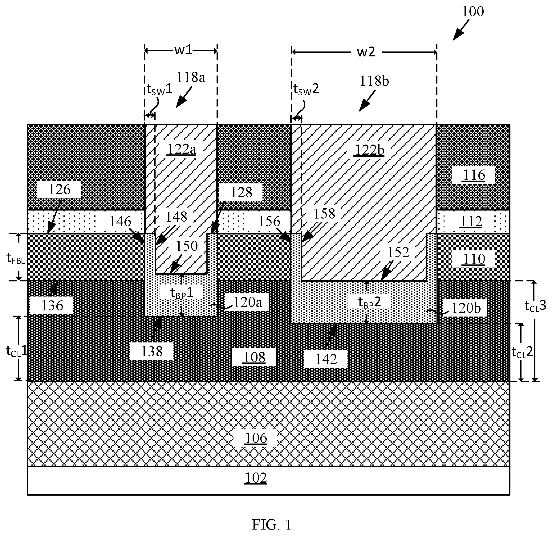
illustrates a cross-sectional view of a transistor structure 100 , according to an embodiment of the disclosure. The structure 100 may be for a high electron mobility transistor. The structure 100 may include a substrate 102 , a buffer layer 106 , a channel layer 108 , a barrier layer 110 , a dielectric cap layer 112 , a dielectric passivation layer 116 , a first gate opening 118 a , a second gate opening 118 b , a first barrier liner 120 a and a first gate electrode 122 a in the first gate opening 118 a , and a second barrier liner 120 b and a second gate electrode 122 b in the second gate opening 118 b . The buffer layer 106 may be arranged over the substrate 102 . The channel layer 108 may be arranged over the buffer layer 106 and may have a top surface 136 in direct contact with the barrier layer 110 . The barrier layer 110 may be arranged above the channel layer 108 and have a top surface 126 in direct contact with the dielectric cap layer 112 . A dielectric passivation layer 116 may be arranged over and directly contacting the dielectric cap layer 112 .
The first gate opening 118 a may be a gate opening of a short channel device, and the first gate opening 118 a may extend through the dielectric passivation layer 116 , the dielectric cap layer 112 , the barrier layer 110 , and partially into the channel layer 108 . The first gate opening 118 a may have sidewalls including side surfaces in the dielectric passivation layer 116 , the dielectric cap layer 112 , the barrier layer 110 and the channel layer 108 . The first gate opening 118 a may also have a bottom surface in the channel layer 108 . The first barrier liner 120 a may have side portions and a lower portion. The side portions of the first barrier liner 120 a may be arranged on part of the sidewalls of the first gate opening 118 a . The lower portion of the first barrier liner 120 a may be arranged on the bottom surface of the first gate opening 118 a . The lower portion of the first barrier liner 120 a may have a bottom surface 138 in contact with the channel layer 108 , and a top surface 150 opposite to the bottom surface 138 . The top surface 150 of the lower portion of the first barrier liner 120 a may be in direct contact with the first gate electrode 122 a . The bottom surface 138 of the first barrier liner 120 a may be lower than a top surface 136 of the channel layer 108 . The barrier layer 110 may have a thickness t FBL taken from the top surface 136 of the channel layer 108 to the top surface 126 of the barrier layer 110 . The lower portion of the first barrier liner 120 a may have a thickness t BP 1 taken from the bottom surface 138 to the top surface 150 . The thickness t FBL of the barrier layer 110 may be approximately the same as the thickness t BP 1 of the lower portion of the first barrier liner 120 a . The thickness t BP 1 may have a range of 4 to 40 nm. The thickness t BP 1 determines a threshold voltage of the short channel device of the structure 100 . Better control of the thickness t BP 1 is achieved, leading to improved reproducibility of the threshold voltage. The barrier liners 120 a and 120 b and the barrier layer 110 may be made of the same material, for example, the same semiconductor material such as aluminum gallium nitride.
The side portions of the first barrier liner 120 a may have a thickness t SW 1 taken from a sidewall 146 to an inner side surface 148 of the first barrier liner 120 a . The sidewall 146 may refer to a side surface of the barrier layer 110 in contact with the side portion of the first barrier liner 120 a . The first gate opening 118 a may have a width w 1 . The thickness t SW 1 may represent a small fraction of the width w 1 and may be less than the thickness t BP 1 . Hence, the side portions of the first barrier liner 120 a do not have a significant effect on the threshold voltage. For example, the thickness t SW 1 may have a range of 2 to 20 nm and the width w 1 may have a range of 50 to 200 nm. A top surface 128 of the side portions of the first barrier liner 120 a may be approximately coplanar with the top surface 126 of the barrier layer 110 . The first barrier liner 120 a may be arranged next to the barrier layer 110 and the channel layer 108 at part of the sidewalls of the first gate opening 118 a and over the channel layer 108 at the bottom surface of the first gate opening 118 a.
A first gate electrode 122 a may be arranged over the first barrier liner 120 a in the first gate opening 118 a . The first barrier liner 120 a may fully separate the first gate electrode 122 a from the barrier layer 110 and the channel layer 108 . The first gate electrode 122 a may be arranged next to the dielectric cap layer 112 and the dielectric passivation layer 116 at another part of the sidewalls of the first gate opening 118 a.
The second gate opening 118 b may be a gate opening for a long channel device and may extend through the dielectric passivation layer 116 , the dielectric cap layer 112 , the barrier layer 110 , and into a part of the channel layer 108 . The second gate opening 118 b may have sidewalls including side surfaces in the dielectric passivation layer 116 , the dielectric cap layer 112 , the barrier layer 110 and the channel layer 108 . The second gate opening 118 b may also have a bottom surface in the channel layer 108 . The second gate opening 118 b may have a width w 2 which may be longer than the width w 1 . For example, the width w 2 may have a range of 200 to 2000 nm. The bottom surface of the second gate opening 118 b may be arranged lower than the bottom surface of the first gate opening 118 a . The second gate opening 118 b may extend further into the channel layer 108 than the first gate opening 118 a.
The second barrier liner 120 b may have side portions and a lower portion. The side portions of the second barrier liner 120 b may be arranged on part of the sidewalls of the second gate opening 118 b . For example, the side portions of the second barrier liner 120 b may be arranged on the side surfaces of the barrier layer 110 . The lower portion of the second barrier liner 120 b may be arranged over the bottom surface of the second gate opening 118 b . The lower portion of the second barrier liner 120 b may have a bottom surface 142 in contact with the channel layer 108 and a top surface 152 opposite to the bottom surface 142 . The bottom surface 142 may be lower than the top surface 136 of the channel layer 108 . The top surface 152 may be in direct contact with the second gate electrode 122 b . A thickness t BP 2 of the lower portion of the second barrier liner 120 b may be taken from the bottom surface 142 to the top surface 152 of the lower portion of the second barrier liner 120 b . The thickness t BP 2 may approximately equal to the thickness t FBL of the barrier layer 110 . In an embodiment, the thickness t BP 2 may be approximately equal to the thickness t BP 1 . The thickness t BP 2 determines a threshold voltage of the long channel device. Better control of the thickness t BP 2 is achieved, leading to improved reproducibility of the threshold voltage.
A portion of the channel layer 108 arranged directly below the second gate opening 118 b may be thinner than another portion of the channel layer 108 arranged directly below the first gate opening 118 a . For example, the channel layer 108 below the first gate opening 118 a has a thickness t CL 1 taken from a top surface of the buffer layer 106 to the bottom surface 138 of the first barrier liner 120 a . The channel layer 108 below the second gate opening 118 b has a thickness t CL 2 , taken from the top surface of the buffer layer 106 to the bottom surface 142 of the second barrier liner 120 b . In one embodiment, t CL 1 may be thicker than t CL 2 . The thickness t CL 2 may be at least 5 to 10 times the thickness t BP 2 of the lower portion of the second barrier liner 120 b . Hence, the channel layer 108 below the second gate opening 118 b may be thicker than the thickness t BP 2 . Additionally, the gate openings 118 a and 118 b may extend into small portions of the channel layer 108 . For example, the channel layer 108 below the barrier layer 110 may have a thickness t CL 3 , taken from the top surface of the buffer layer 106 to the top surface 136 of the channel layer 108 , in the range of 150 to 500 nm. Hence the formation of the gate openings 118 a and 118 b in part of the channel layer 108 do not affect the operation of the short channel and long channel devices, respectively.
The side portions of the second barrier liner 120 b may have a thickness t SW 2 , taken from a sidewall 156 of the second gate opening 118 b to an inner side surface 158 of the second barrier liner 120 b . The sidewall 156 may refer to a side surface of the barrier layer 110 in contact with the side portion of the second barrier liner 120 b . The thickness t SW 2 of the side portions may be thinner than the thickness t BP 2 of the lower portion. Additionally, the thickness t SW 2 may be thinner than the width w 2 of the second gate opening 118 b . Hence, the side portions of the second barrier liner 120 b do not affect the threshold voltage of the long channel device.
A second gate electrode 122 b may be arranged over the second barrier liner 120 b in the second gate opening 118 b , whereby the second gate electrode 122 b may be fully separated from the barrier layer 110 and the channel layer 108 by the second barrier liner 120 b . The gate electrodes 122 a and 122 b may fill up the gate openings 118 a and 118 b , respectively. The gate electrodes 122 a and 122 b may be gate contacts for the short channel and the long channel devices, respectively. Although not shown for simplicity, a source and a drain may be formed in the barrier layer 110 and arranged next to the sides of each of the gate openings 118 a and 118 b.
The substrate 102 may be made of silicon, silicon carbide, graphene, diamond, sapphire, or any composite substrate suitable for gallium nitride/aluminum gallium nitride epitaxy and the buffer layer 106 may be made of aluminum gallium nitride and aluminum nitride superlattices. The channel layer 108 may be made of gallium nitride in a preferred embodiment. In an alternative embodiment, the channel layer 108 may be made of carbon-doped gallium nitride (C-GaN) and gallium nitride. The barrier layer 110 may be made of aluminum gallium nitride in a preferred embodiment. In an alternative embodiment, the barrier layer 110 may be made of aluminum nitride or a combination of aluminum gallium nitride and aluminum nitride. The dielectric cap layer 112 may be made of silicon nitride, silicon carbon, or any other suitable dielectric material. The dielectric passivation layer 116 may be made of silicon dioxide, carbon doped oxide dielectrics comprised of silicon, carbon, oxygen, and hydrogen (SiCOH), or any other suitable dielectric material. The gate electrodes 122 a and 122 b may be made of titanium nitride, tantalum nitride, aluminum, copper, nickel, or its combination.
The embodiments shown in may be modified to form alternative embodiments without departing from the scope of the disclosure. For example, illustrates a cross-sectional view of a transistor structure 200 , according to another embodiment of the disclosure. Like numerals in may refer to like features in . In contrast to the structure 100 , the structure 200 shows a first gate dielectric layer 232 a separating a first gate electrode 122 a from a first barrier liner 120 a in a first gate opening 118 a . Additionally, the structure 200 shows a second gate dielectric layer 232 b between a second gate electrode 122 b and a second barrier liner 120 b in a second gate opening 118 b . The gate dielectric layers 232 a and 232 b may electrically insulate the gate electrodes, 122 a and 122 b , respectively, from the barrier liners, 120 a and 120 b , respectively. The gate dielectric layers 232 a and 232 b may be made of an oxide of aluminum. The structure 200 may be for a metal insulator semiconductor high electron mobility transistor (MIS-HEMT). An advantage of the structure 200 may be due to lower leakage current.
to 4 illustrate a fabrication process flow for the transistor structure 100 shown in , according to some embodiments of the disclosure. illustrates a cross-sectional view of a partially completed transistor structure 100 after formation of a channel layer 108 , a barrier layer 110 , a dielectric cap layer 112 , a dielectric passivation layer 116 , and gate openings 118 a and 118 b , according to an embodiment of the disclosure. Referring to , the channel layer 108 may be formed over a buffer layer 106 arranged above a substrate 102 . The channel layer 108 may be formed by epitaxial growth, molecular beam epitaxy, metal oxide chemical vapor deposition, plasma assisted molecular beam epitaxy, or any other suitable process. The barrier layer 110 may be formed over the channel layer 108 by epitaxial growth, molecular beam epitaxy, metal oxide chemical vapor deposition, plasma assisted molecular beam epitaxy, or any other suitable process. The dielectric cap layer 112 may be deposited over the barrier layer 110 and the dielectric passivation layer 116 may be deposited over the dielectric cap layer 112 . The dielectric cap layer 112 and the dielectric passivation layer 116 may be deposited by atomic layer deposition, chemical vapor deposition, physical vapor deposition, or any other suitable deposition processes. The gate openings 118 a and 118 b may be formed by patterning the dielectric passivation layer 116 , dielectric cap layer 112 , barrier layer 110 and channel layer 108 by a photolithography process. In the photolithography process, a photoresist layer may be deposited over a top surface of the dielectric passivation layer 116 and subsequently exposed and developed to form a suitable photoresist pattern. A wet or dry etch process may be used to remove portions of the dielectric passivation layer 116 , dielectric cap layer 112 , barrier layer 110 and channel layer 108 not covered by the photoresist pattern to form the gate openings 118 a and 118 b . The etching processes may etch through the dielectric passivation layer 116 , dielectric cap layer 112 , and barrier layer 110 and partially etch into the channel layer 108 . The other portions of the dielectric passivation layer 116 , dielectric cap layer 112 , barrier layer 110 and channel layer 108 below the photoresist pattern may be left behind. The photoresist pattern may subsequently be removed. The first gate opening 118 a may be shallower than the second gate opening 118 b.
illustrates a cross-sectional view of a partially completed transistor structure 100 after formation of barrier liners 120 a and 120 b in the gate openings 118 a and 118 b , respectively, according to an embodiment of the disclosure. The barrier liners 120 a and 120 b may be selectively grown on the barrier layer 110 and the channel layer 108 at sidewalls of the gate openings 118 a and 118 b , respectively. Additionally, the barrier liners 120 a and 120 b may be selectively grown on the channel layer 108 at bottom surfaces of the gate openings 118 a and 118 , respectively. The barrier liners 120 a and 120 b may be selectively grown by an epitaxial process.
The fabrication process may continue to form the transistor structure 100 illustrated in . Referring to , a layer of a suitable metal, for example, titanium nitride, tantalum nitride, aluminum, copper, nickel or its combination, may be deposited over the barrier liners 120 a and 120 b in the gate openings 118 a and 118 b , respectively. The metal may be deposited by electroplating, atomic layer deposition, physical vapor deposition, chemical vapor deposition, plasma enhanced chemical vapor deposition, or any other suitable deposition processes. A suitable planarization process, for example, chemical mechanical planarization, may remove portions of the metal from a top surface of the dielectric passivation layer 116 next to the openings 118 a and 118 b . The process may leave behind other portions of the metal in the gate openings 118 a and 118 b , thereby forming the gate electrodes 122 a and 122 b , respectively.
illustrates a partially completed transistor structure 200 shown in after formation of a channel layer 108 , a barrier layer 110 , a dielectric cap layer 112 , a dielectric passivation layer 116 , gate openings 118 a and 118 b , barrier liners 120 a and 120 b , and gate dielectric layers 232 a and 232 b , according to an embodiment of the disclosure. The channel layer 108 may be formed over the buffer layer 106 arranged above the substrate 102 . The formation of the channel layer 108 for the structure 200 may be like the formation of the channel layer 108 for the structure 100 shown in . The formation of the barrier layer 110 , dielectric cap layer 112 , dielectric passivation layer 116 , and gate openings 118 a and 118 b of the structure 200 may be like the formation of like features of the structure 100 shown in . The formation of the barrier liners 120 a and 120 b of the structure 200 may be like the formation of like features of the structure 100 shown in . The first gate dielectric layer 232 a may be uniformly deposited on side portions and a lower portion of the first barrier liner 120 a . Additionally, the second gate dielectric layer 232 b may be uniformly deposited on side portions and a lower portion of the second barrier liner 120 b . Although not shown, the gate dielectric layers 232 a and 232 b may be deposited on the dielectric cap layer 112 and dielectric passivation layer 116 above the barrier liners 120 a and 120 b . The gate dielectric layers 232 a and 232 b may be deposited by atomic layer deposition, chemical vapor deposition, physical vapor deposition or any other suitable deposition processes.
The process may continue to form the transistor structure 200 shown in . Referring to , a first gate electrode 122 a may be deposited over the first gate dielectric layer 232 a , thereby filling up the first gate opening 118 a . A second gate electrode 122 b may be deposited over the second gate dielectric layer 232 b , thereby filling up the second gate opening 118 b . The fabrication of the gate electrodes 122 a and 122 b of the structure 200 may be like the fabrication of like features of the structure 100 shown in .
The terms “first”, “second”, “third”, and the like in the description and in the claims, if any, are used for distinguishing between similar elements and not necessarily for describing a particular sequential or chronological order. It is to be understood that the terms so used are interchangeable under appropriate circumstances such that the embodiments of the device described herein are, for example, capable of operation in sequences other than those illustrated or otherwise described herein. The terms “left”, “right”, “front”, “back”, “top”, “bottom”, “over”, “under”, and the like in the description and in the claims, if any, are used for descriptive purposes and not necessarily for describing permanent relative positions. It is to be understood that the terms so used are interchangeable under appropriate circumstances such that the embodiments of the device described herein are, for example, capable of operation in other orientations than those illustrated or otherwise described herein. Similarly, if a method is described herein as comprising a series of steps, the order of such steps as presented herein is not necessarily the only order in which such steps may be performed, and certain of the stated steps may possibly be omitted and/or certain other steps not described herein may possibly be added to the method. Furthermore, the terms “comprise”, “include”, “have”, and any variations thereof, are intended to cover a non-exclusive inclusion, such that a process, method, article, or device that comprises a list of elements is not necessarily limited to those elements, but may include other elements not expressly listed or inherent to such process, method, article, or device.
While several exemplary embodiments have been presented in the above detailed description of the device, it should be appreciated that number of variations exist. It should further be appreciated that the embodiments are only examples, and are not intended to limit the scope, applicability, dimensions, or configuration of the devices in any way. Rather, the above detailed description will provide those skilled in the art with a convenient road map for implementing an exemplary embodiment of the devices, it being understood that various changes may be made in the function and arrangement of elements and method of fabrication described in an exemplary embodiment without departing from the scope of this disclosure as set forth in the appended claims.
Figures (5)
Citations
This patent cites (11)
- US7592211
- US7772676
- US9318593
- US10396192
- US10644128
- US2005/0258451
- US2012/0313106
- US2019/0189762
- US2021/0234030
- US1865561
- US20140014778