Abstract
A memory array includes at least one strap region, at least two sub-arrays, a plurality of staggered, dummy magnetic storage elements, and a plurality of bit line structures. The strap region includes a plurality of source line straps and a plurality of word line straps. The two sub-arrays include a plurality of staggered, active magnetic storage elements. The two sub-arrays are separated by the strap region. The staggered, dummy magnetic storage elements are disposed within the strap region. The bit line structures are disposed in the two sub-arrays, and each of the bit line structures is disposed above and directly connected with at least one of the staggered, active magnetic storage elements.
Claims (19)
1. A memory array, comprising: at least one strap region comprising a plurality of source line straps and a plurality of word line straps; at least two sub-arrays comprising a plurality of staggered, active magnetic storage elements, wherein the at least two sub-arrays are separated by the strap region; a plurality of staggered, dummy magnetic storage elements disposed within the strap region; and a plurality of bit line structures disposed in the at least two sub-arrays, wherein each of the plurality of bit line structures is disposed above and directly connected with at least one of the plurality of staggered, active magnetic storage elements, wherein each of the plurality of bit line structures comprises: a first bit line; and a second bit line disposed above the first bit line, wherein the first bit line and the second bit line are elongated in the same direction and electrically connected with each other.
Show 18 dependent claims
2. The memory array according to claim 1 , wherein each of the plurality of bit line structures is directly connected with at least two of the plurality of staggered, active magnetic storage elements aligned in the same row.
3. The memory array according to claim 1 , wherein each of the plurality of bit line structures further comprises: at least one conductive via disposed between the first bit line and the second bit line, wherein the first bit line is electrically connected with the second bit line through the at least one conductive via.
4. The memory array according to claim 1 , wherein a top electrode of at least one of the plurality of staggered, dummy magnetic storage elements is electrically connected with one of the plurality of word line straps through a pad disposed on the at least one of the plurality of staggered, dummy magnetic storage elements.
5. The memory array according to claim 4 , wherein the pad is a portion of a metal layer, each of the first bit lines is another portion of the metal layer, and the pad is separated from the first bit lines.
6. The memory array according to claim 1 , wherein the plurality of source line straps comprises a plurality of first source line straps extending in a first direction and a plurality of second source line straps extending in the first direction.
7. The memory array according to claim 6 , wherein the plurality of word line straps extends in the first direction and is located between the plurality of first source line straps and the plurality of second source line straps in a second direction.
8. The memory array according to claim 7 , wherein the first direction is orthogonal to the second direction.
9. The memory array according to claim 7 , wherein each of the plurality of first source line straps is connected to a common source line extending in the second direction.
10. The memory array according to claim 7 , further comprising: a first dummy diffusion region extending in the first direction, wherein the first dummy diffusion region is disposed directly under the plurality of first source line straps.
11. The memory array according to claim 10 , further comprising: a second dummy diffusion region extending in the first direction, wherein the second dummy diffusion region is disposed directly under the plurality of second source line straps.
12. The memory array according to claim 11 , further comprising: a third dummy diffusion region extending in the first direction, wherein the third dummy diffusion region is disposed directly under the plurality of word line straps, and the third dummy diffusion region is located between the first dummy diffusion region and the second dummy diffusion region in the second direction.
13. The memory array according to claim 7 , further comprising: a plurality of gate lines extending in the second direction.
14. The memory array according to claim 13 , wherein the plurality of staggered, active magnetic storage elements comprises a plurality of first active magnetic storage elements arranged in a first column and a plurality of second active magnetic storage elements arranged in a second column, wherein the plurality of first active magnetic storage elements arranged in the first column and the plurality of second active magnetic storage elements arranged in the second column are aligned with the plurality of gate lines extending in the second direction, respectively.
15. The memory array according to claim 1 , wherein each of the plurality of staggered, active magnetic storage elements is electrically connected to a storage node pad through a tungsten via.
16. The memory array according to claim 1 , wherein no tungsten via is disposed within the strap region.
17. The memory array according to claim 1 , wherein the plurality of staggered, dummy magnetic storage elements comprises dummy magnetic tunneling junction (MTJ) elements.
18. The memory array according to claim 17 , wherein bottom electrodes of the dummy MTJ elements are not electrically connected to the plurality of source line straps or the plurality of word line straps.
19. The memory array according to claim 1 , wherein the plurality of staggered, active magnetic storage elements and the plurality of staggered, dummy magnetic storage elements are uniformly distributed in the at least two sub-arrays and the strap region.
Full Description
Show full text →
BACKGROUND OF THE INVENTION
1. Field of the Invention
The present invention relates to a semiconductor device, in particular to a high-density magnetoresistive random access memory (MRAM) array.
2. Description of the Prior Art
Magnetoresistance (MR) effect has been known as a kind of effect caused by altering the resistance of a material through variation of outside magnetic field. The physical definition of such effect is defined as a variation in resistance obtained by dividing a difference in resistance under no magnetic interference by the original resistance. Currently, MR effect has been successfully utilized in production of hard disks thereby having important commercial values. Moreover, the characterization of utilizing GMR materials to generate different resistance under different magnetized states could also be used to fabricate MRAM devices, which typically has the advantage of keeping stored data even when the device is not connected to an electrical source.
The aforementioned MR effect has also been used in magnetic field sensor areas including but not limited to for example electronic compass components used in global positioning system (GPS) of cellular phones for providing information regarding moving location to users. Currently, various magnetic field sensor technologies such as anisotropic magnetoresistance (AMR) sensors, GMR sensors, magnetic tunneling junction (MTJ) sensors have been widely developed in the market. Nevertheless, most of these products still pose numerous shortcomings such as high chip area, high cost, high power consumption, limited sensibility, and easily affected by temperature variation and how to come up with an improved device to resolve these issues has become an important task in the related field.
SUMMARY OF THE INVENTION
It is one object of the present invention to provide a high-density magnetoresistive random access memory (MRAM) array to solve the above-mentioned shortcomings or deficiencies of the prior art.
According to one aspect of the present invention, a memory array includes at least one strap region including a plurality of source line straps and a plurality of word line straps; at least two sub-arrays including a plurality of staggered, active magnetic storage elements, wherein the at least two sub-arrays are separated by the strap region; a plurality of staggered, dummy magnetic storage elements disposed within the strap region; and a plurality of bit line structures disposed in the at least two sub-arrays, wherein each of the plurality of bit line structures is disposed above and directly connected with at least one of the plurality of staggered, active magnetic storage elements.
According to some embodiments of the present invention, each of the plurality of bit line structures is directly connected with at least two of the plurality of staggered, active magnetic storage elements aligned in the same row.
According to some embodiments of the present invention, each of the plurality of bit line structures includes a first bit line and a second bit line disposed above the first bit line, and the first bit line and the second bit line are elongated in the same direction and electrically connected with each other.
According to some embodiments of the present invention, each of the plurality of bit line structures further includes at least one conductive via disposed between the first bit line and the second bit line, wherein the first bit line is electrically connected with the second bit line through the at least one conductive via.
According to some embodiments of the present invention, a top electrode of at least one of the plurality of staggered, dummy magnetic storage elements is electrically connected with one of the plurality of word line straps through a pad disposed on the at least one of the plurality of staggered, dummy magnetic storage elements.
According to some embodiments of the present invention, the pad is a portion of a metal layer, each of the first bit lines is another portion of the metal layer, and the pad is separated from the first bit lines.
According to some embodiments of the present invention, the plurality of source line straps includes a plurality of first source line straps extending in a first direction and a plurality of second source line straps extending in the first direction.
According to some embodiments of the present invention, the plurality of word line straps extends in the first direction and is located between the plurality of first source line straps and the plurality of second source line straps in a second direction
According to some embodiments of the present invention, the first direction is orthogonal to the second direction.
According to some embodiments of the present invention, each of the plurality of first source line straps is connected to a common source line extending in the second direction.
According to some embodiments of the present invention, the memory array further includes a first dummy diffusion region extending in the first direction, and the first dummy diffusion region is disposed directly under the plurality of first source line straps.
According to some embodiments of the present invention, the memory array further includes a second dummy diffusion region extending in the first direction, and the second dummy diffusion region is disposed directly under the plurality of second source line straps.
According to some embodiments of the present invention, the memory array further includes a third dummy diffusion region extending in the first direction, the third dummy diffusion region is disposed directly under the plurality of word line straps, and the third dummy diffusion region is located between the first dummy diffusion region and the second dummy diffusion region in the second direction.
According to some embodiments of the present invention, the memory array further includes a plurality of gate lines extending in the second direction.
According to some embodiments of the present invention, the plurality of staggered, active magnetic storage elements includes a plurality of first active magnetic storage elements arranged in a first column and a plurality of second active magnetic storage elements arranged in a second column, wherein the plurality of first active magnetic storage elements arranged in the first column and the plurality of second active magnetic storage elements arranged in the second column are aligned with the plurality of gate lines extending in the second direction, respectively.
According to some embodiments of the present invention, each of the plurality of staggered, active magnetic storage elements is electrically connected to a storage node pad through a tungsten via.
According to some embodiments of the present invention, no tungsten via is disposed within the strap region.
According to some embodiments of the present invention, the plurality of staggered, dummy magnetic storage elements includes dummy magnetic tunneling junction (MTJ) elements.
According to some embodiments of the present invention, bottom electrodes of the dummy MTJ elements are not electrically connected to the plurality of source line straps or the plurality of word line straps.
According to some embodiments of the present invention, the plurality of staggered, active magnetic storage elements and the plurality of staggered, dummy magnetic storage elements are uniformly distributed in the at least two sub-arrays and the strap region.
These and other objectives of the present invention will no doubt become obvious to those of ordinary skill in the art after reading the following detailed description of the preferred embodiment that is illustrated in the various figures and drawings.
BRIEF DESCRIPTION OF THE DRAWINGS
is a schematic diagram of a memory array according to an embodiment of the present invention, which mainly shows active areas, polysilicon gate lines, and common source lines, source line straps and word line straps located in the first metal layer.
is a schematic diagram of a memory array according to an embodiment of the present invention, which mainly shows the positions of conductive vias, storage node pads, and tungsten vias.
is a schematic diagram of a memory array according to an embodiment of the present invention, which mainly shows the positions of magnetic storage elements.
is a schematic diagram of a memory array according to an embodiment of the present invention, which mainly shows the position of conductive via in the strap region.
is a schematic diagram of a memory array according to an embodiment of the present invention, which mainly shows the positions of the first bit lines and the pads located in the third metal layer in the strap region.
is a schematic diagram of a memory array according to an embodiment of the present invention, which mainly shows the layout of the conductive vias located on the third metal layer.
is a schematic diagram of a memory array according to an embodiment of the present invention, which mainly shows the layout of the fourth metal layer.
is a schematic diagram of a memory array according to an embodiment of the present invention, which mainly shows the layout of the conductive vias located on the fourth metal layer.
is a schematic diagram of a memory array according to an embodiment of the present invention, which mainly shows the layout of the fifth metal layer.
is a schematic cross-sectional diagram of part of the structure in a sub-array of a memory array according to an embodiment of the present invention.
is another schematic cross-sectional diagram of part of the structure in a sub-array of a memory array according to an embodiment of the present invention.
is a three-dimensional schematic diagram of part of the structure in a sub-array of a memory array according to an embodiment of the present invention.
is a three-dimensional schematic diagram of a part of the structure in a sub-array and a strap region of a memory array according to an embodiment of the present invention.
DETAILED DESCRIPTION
In the following detailed description of the disclosure, reference is made to the accompanying drawings, which form a part hereof, and in which is shown, by way of illustration, specific embodiments in which the invention may be practiced. These embodiments are described in sufficient detail to enable those skilled in the art to practice the invention.
Other embodiments may be utilized and structural, logical, and electrical changes may be made without departing from the scope of the present invention. Therefore, the following detailed description is not to be considered as limiting, but the embodiments included herein are defined by the scope of the accompanying claims.
The present invention pertains to a high-density memory layout, in particular a high-density magnetoresistive random access memory (MRAM) array. The special technical features includes: a plurality of staggered dummy magnetic storage elements may be arranged in a strap region between two sub-arrays, so that the active magnetic storage elements and the dummy magnetic storage elements of the memory array are evenly distributed in the two sub-arrays and the strap region in a staggered arrangement. Therefore, a high-density memory layout can be realized. In addition, the influence of the conductive via directly contacting the active magnetic storage element on the alignment deviation may be avoided by disposing the bit line structure in the sub-array, wherein the bit line structure is disposed above and directly contacts the active magnetic storage element. The related manufacturing yield may be enhanced accordingly.
In the following detailed description, metal layers Mn represent the different metal layers in the metal interconnect structure, where n is a positive integer. For example, the metal layer M 1 represents the first metal layer in the metal interconnect structure, and the metal layer M 2 represents the second metal layer in the metal interconnect structure, and so on. The conductive vias Vn represent the different conductive vias in the metal interconnection structure. For example, the conductive via V 1 represents the conductive via connecting the metal layer M 1 to the metal layer M 2 , and the conductive via V 2 represents the conductive via connecting the metal layer M 2 to the metal layer M 3 , and so on. Different objects formed of the same metal layer (and/or the metal layer at the same level) may be regarded as being located in the same metal layer, and the different objects located in the same metal layer may be separated from one another or connected with one another according to some design considerations.
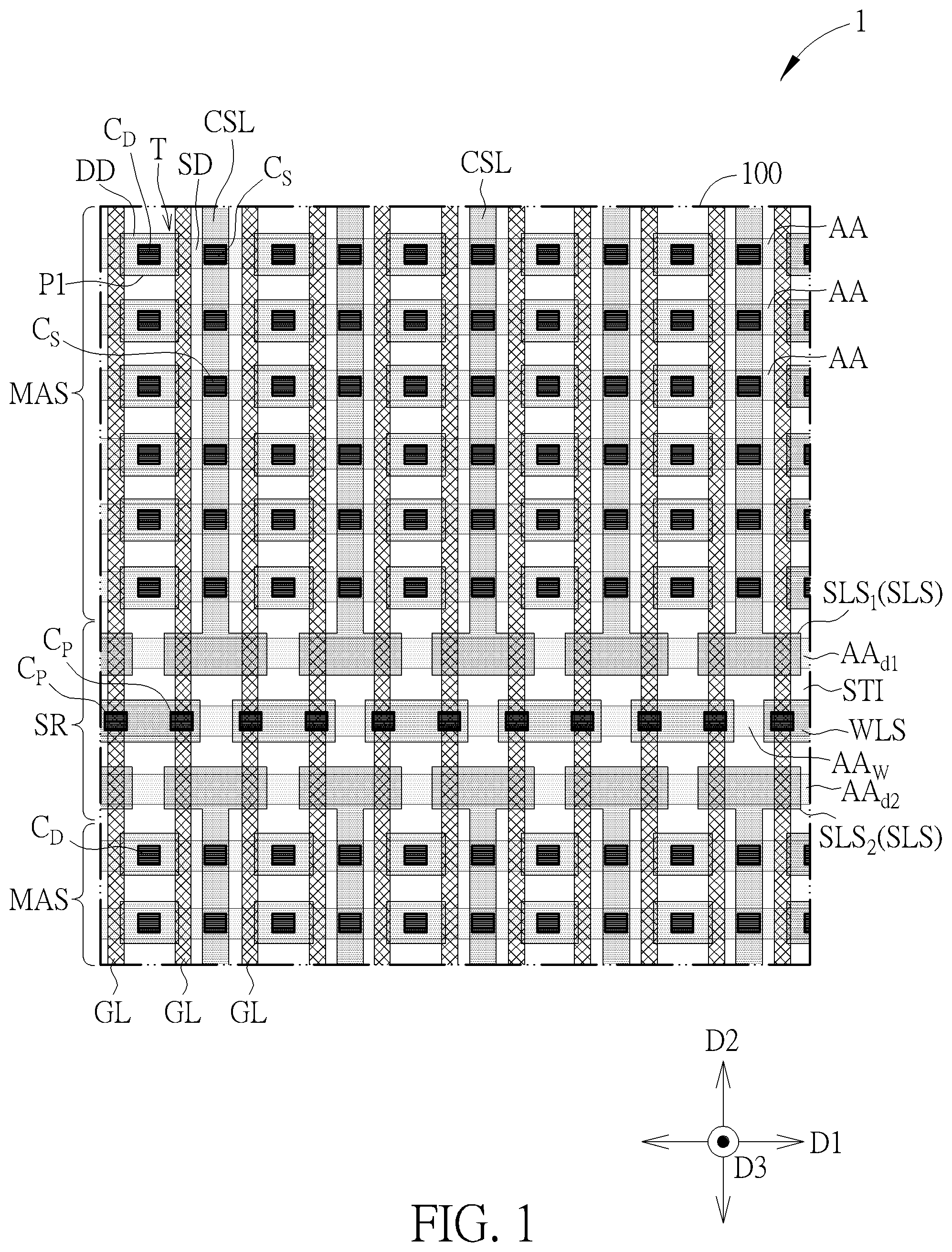
Please refer to , which is a schematic diagram of a memory array according to an embodiment of the present invention, which mainly shows active areas, polysilicon gate lines, and common source lines, source line straps, and word line straps located in the first metal layer (such as the metal layer M 1 ). As shown in , the memory array 1 includes at least two sub-arrays MAS and at least one strap region SR. According to an embodiment of the present invention, the strap region SR is a strip-shaped region extending in a first direction D1, and the two sub-arrays MAS are separated by the strap region SR. According to an embodiment of the present invention, the memory array 1 further includes a plurality of gate lines (such as polysilicon gate lines GL) extending in a second direction D2 and a plurality of active areas AA extending in the first direction D1 formed in a semiconductor substrate 100 . According to an embodiment of the present invention, the first direction D1 is orthogonal to the second direction D2. According to an embodiment of the present invention, the active areas AA are isolated from one another by the shallow trench isolation areas STI.
According to an embodiment of the present invention, the polysilicon gate lines GL pass through the two sub-arrays MAS and the strap region SR, and form transistors T at the intersections between the polysilicon gate lines GL and the active areas AA in the sub-array MAS. According to an embodiment of the present invention, the transistor T includes a source region SD and a drain region DD, for example, an N + doped region, but not limited thereto. According to an embodiment of the present invention, a first dummy diffusion region AA d1 and a second dummy diffusion region AA d2 extending in the first direction D1, which are respectively adjacent to the two sub-arrays MAS, and a third dummy diffusion region AA W located between first dummy diffusion region AA d1 and the second dummy diffusion region AA d2 in the second direction D2 are further provided in the strap region SR. According to an embodiment of the present invention, the first dummy diffusion region AA d1 , the second dummy diffusion region AA d2 , the third dummy diffusion region AA W , and the active areas AA are semiconductor regions located in the semiconductor substrate 100 and defined by the shallow trench isolation areas STI. According to an embodiment of the present invention, the first dummy diffusion region AA d1 , the second dummy diffusion region AA d2 , and the third dummy diffusion region AA W may help improve the manufacturing yield of memory cells located at the edge of the sub-arrays MAS.
According to an embodiment of the present invention, a plurality of source line straps SLS and a plurality of word line straps WLS located in the first metal layer are further provided in the strap region SR. The plurality of source line straps SLS includes a plurality of first source line straps SLS 1 extending in the first direction D1 and a plurality of second source line straps SLS 2 extending in the first direction D1. According to an embodiment of the present invention, the plurality of first source line straps SLS 1 are substantially aligned with the first dummy diffusion region AA d1 , the plurality of second source line straps SLS 2 are substantially aligned with the second dummy diffusion region AA d2 , and the plurality of word line straps WLS are substantially aligned with the third dummy diffusion region AA W . In other words, the first dummy diffusion region AA d1 may be disposed directly under the plurality of first source line straps SLS 1 in a third direction D3, the second dummy diffusion region AA d2 may be disposed directly under the plurality of second source line straps SLS 2 in the third direction D3, and the third dummy diffusion region AA W may be disposed directly under the plurality of word line straps WLS in the third direction D3. According to an embodiment of the present invention, the third direction D3 may be regarded as a vertical direction and may be orthogonal to the first direction D1 and the second direction D2. According to an embodiment of the present invention, the width of the first dummy diffusion region AA d1 , the width of the second dummy diffusion region AA d2 , the width of the third dummy diffusion region AA W may, and the spacing between the first dummy diffusion region AA d1 , the second dummy diffusion region AA d2 , and third dummy diffusion region AA W in the second direction D2 may be substantially equal to the width of each active area AA and the spacing between the active areas AA in the second direction, so as to improve related manufacturing uniformity and/or enhance relative manufacturing yield.
According to an embodiment of the present invention, a plurality of word line straps WLS, which is also located in the first metal layer, may be provided in the strap region SR. According to an embodiment of the present invention, in the second direction D2, the plurality of first source line straps SLS 1 extending in the first direction D1 and the plurality of second source line straps SLS 2 extending in the first direction D1 sandwich about the plurality of word lines straps WLS extend in the first direction D1. Therefore, the plurality of word lines straps WLS is located between the plurality of first source line straps SLS 1 and the plurality of second source line straps SLS 2 in the second direction D2. According to an embodiment of the present invention, the word line strap WLS, the first source line strap SLS 1 and the second source line strap SLS 2 are arranged in a staggered manner. According to an embodiment of the present invention, each word line strap WLS is electrically connected to two adjacent polysilicon gate lines GL through two contact plugs C P .
According to an embodiment of the present invention, the first source line straps SLS 1 are respectively connected to the common source line CSL extending in the second direction D2. According to an embodiment of the present invention, the common source line CSL is electrically connected to the source regions SD of the transistors T through the source contact plugs C S , respectively. According to an embodiment of the present invention, the memory array 1 further includes a plurality of pads P 1 located on the drain regions DD of the transistors T and electrically connected to the drain regions DD of the transistors T through the drain contact plugs C D , respectively. According to an embodiment of the present invention, the pads P 1 and the common source lines CSL may also be located in the first metal layer. In other words, the word line straps WLS, the source line straps SLS, the pads P 1 , and the common source lines CSL may be different portions of the first metal layer (such as the metal layer M 1 ).
Please refer to , which is a schematic diagram of a memory array according to an embodiment of the present invention, which mainly shows the positions of conductive vias, storage node pads, and tungsten vias. As shown in , the memory array 1 further includes a plurality of conductive vias V 1 , and the conductive vias V 1 may include a conductive via V A1 provided on each of the pads P 1 in the sub-arrays MAS, a conductive via V S1 on each of the first source line straps SLS 1 , a conductive via V S2 on each of the second source line straps SLS 2 , and a conductive via V W on each of the word line straps WLS in the strap region SR. According to an embodiment of the present invention, a width (or a length) of the conductive via V S1 , a width (or a length) of the conductive via V S2 , and a width (or a length) of the conductive via V W in the first direction D1 may be greater than a width (or a length) of the conductive via V A1 in the first direction D1.
According to an embodiment of the present invention, the memory array 1 further includes a plurality of storage node pads P 2 in the sub-arrays MAS, which are electrically connected to the conductive vias V A1 , respectively, and located in the second metal layer (such as the metal layer M 2 ), pads P S1 electrically connected to the conductive vias V S1 in the strap region SR, pads P S2 electrically connected to the conductive vias V S2 in the strap region SR, and pads P W electrically connected to the conductive vias V W in the strap region SR. According to an embodiment of the present invention, each of the storage node pads P 2 may have a rectangular outline, the long side of which is parallel to the first direction D1. Each of the storage node pads P 2 may partially overlap the underlying polysilicon gate lines GL. According to an embodiment of the present invention, the storage node pad P 2 , the pad P S1 , the pad P S2 , and the pad P W may be both located in the second metal layer. In other words, the storage node pad P 2 , the pad P S1 , the pad P S2 , and the pad P W may be different portions of the second metal layer (such as the metal layer M 2 ). According to an embodiment of the present invention, the memory array 1 further includes a plurality of tungsten vias 140 in the sub-arrays MAS, which are respectively electrically connected to the corresponding storage node pads P 2 . According to an embodiment of the present invention, the plurality of tungsten vias 140 may be arranged in a staggered arrangement and may be substantially aligned with the polysilicon gate lines GL below. According to an embodiment of the present invention, no tungsten vias are arranged on the pads P S1 , the pads P S2 , and the pads P W in the strap region SR.
Please refer to and , which is a schematic diagram of a memory array according to an embodiment of the present invention, which mainly shows the position of the magnetic storage elements. As shown in and , the sub-array MAS of the memory array 1 includes a plurality of staggered active magnetic storage elements M A , and the strap region SR includes a plurality of staggered dummy magnetic storage elements M D . According to an embodiment of the present invention, in the sub-arrays MAS, the active magnetic storage elements M A are disposed on the corresponding tungsten vias 140 , that is, the active magnetic storage elements M A are substantially aligned with the corresponding tungsten vias 140 , respectively, and are approximately aligned with the underlying polysilicon gate lines GL, respectively. The active magnetic storage elements M A are electrically connected to the storage node pads P 2 , respectively, through the tungsten vias 140 .
According to an embodiment of the present invention, the active magnetic storage elements M A include a plurality of first active magnetic storage elements M A1 arranged in a first column and a plurality of second active magnetic storage elements M A2 arranged in a second column. The first active magnetic storage elements M A1 arranged in the first column and the second active magnetic storage elements M A2 arranged in the second column are respectively aligned with corresponding polysilicon gate lines GL extending in the second direction D2.
According to an embodiment of the present invention, each of the active magnetic storage elements M A and the dummy magnetic storage elements M D may include a magnetic tunnel junction (MTJ) element. According to an embodiment of the present invention, the MTJ element may include a multilayer structure, for example, a bottom electrode, a top electrode, and a magnetic tunnel junction structure between the bottom electrode and the top electrode. The magnetic tunnel junction structure may include, but not limited to, a reference layer, a channel layer, a free layer and a cap layer. According to an embodiment of the present invention, the bottom electrode of the MTJ element (dummy MTJ element) of the dummy magnetic storage element M D is not electrically connected to the source line strap or the word line strap.
According to an embodiment of the present invention, the dummy magnetic storage elements M D are respectively arranged on the pads P S1 , the pads P S2 and the pads P W in the strap region SR in a staggered manner. Since there are no tungsten vias arranged on the pads P S1 , the pads P S2 , and the pads P W in the strap region SR, the bottom electrode of the dummy magnetic storage element M D will not be directly electrically connected to the pads P S1 , the pads P S2 , and the pads P W in the strap region SR. According to an embodiment of the present invention, there are only dielectric layers between the dummy magnetic storage element M D and the pad P S1 , between the dummy magnetic storage element M D and the pad P S2 , and between the dummy magnetic storage element M D and the pad P W .
According to an embodiment of the present invention, the staggered active magnetic storage elements M A and the staggered dummy magnetic storage elements M D are evenly distributed on the two sub-arrays MAS and the strap region SR. Such a uniform and repeated arrangement of magnetic storage elements can specifically realize a high-density memory layout.
Please refer to , which is a schematic diagram of a memory array according to an embodiment of the present invention, which mainly shows the position of the conductive via (such as the conductive vias V 2 ) in the strap region SR. As shown in , the memory array 1 is additionally provided with staggered conductive vias V PS1 , conductive vias V PW , and conductive vias V PS2 in the strap region SR. The conductive vias V PS1 , conductive vias V PW , and conductive vias V PS2 are electrically connected to the pads P S1 , the pads P W , and the pads P S2 located underneath, respectively.
Please refer to , which is a schematic diagram of a memory array according to an embodiment of the present invention, which mainly shows the positions of the pads located on the third metal layer (such as the metal layer M 3 ) in the strap region SR and the first bit lines. As shown in , the memory array 1 is additionally provided with pads P VS1 , pads P VW , and pads P VS2 located in the third metal layer in the strap region SR. The dimensions and the positions of the pads P VS1 , the pads P VW , and the pads P VS2 may be substantially the same as the underlying first source line strap SLS 1 , the word line strap WLS, and the second source line strap SLS 2 .
As shown in , the memory array 1 further includes a plurality of first bit lines BL 1 disposed in the two sub-arrays MAS, and each of the first bit lines BL 1 may be disposed above and directly connected with the corresponding active magnetic storage element M A . According to an embodiment of the present invention, each of the first bit lines BL 1 may extend in the first direction D1 and be a portion of a bit line structure BS. Therefore, the memory array 1 may include a plurality of bit line structures BS disposed above and directly connected with the corresponding active magnetic storage elements M A . For example, each of the first bit lines BL 1 may extend in the first direction D1 and may be disposed above and directly connected with the active magnetic storage elements M A arranged in the same row. Therefore, each of the bit line structures BS may be directly connected with the active magnetic storage elements M A arranged in the same row.
According to an embodiment of the present invention, the pad P VS1 covers the conductive via V PS1 and the adjacent dummy magnetic storage element M D , and electrically connects the top electrode of the dummy magnetic storage element M D to the conductive via V PS1 . According to an embodiment of the present invention, the pad P VS2 covers the conductive via V PS2 and the adjacent dummy magnetic storage element M D , and electrically connects the top electrode of the dummy magnetic storage element M D to the conductive via V PS2 . According to an embodiment of the present invention, the pad P VW covers the conductive via V PW and the adjacent dummy magnetic storage element M D , and electrically connects the top electrode of the dummy magnetic storage element M D to the conductive via V PW . In other words, a part of the pad P VS1 may be disposed on the dummy magnetic storage element M D located on the first source line strap SLS 1 , a part of the pad P VS2 may be disposed on the dummy magnetic storage element M D located on the second source line strap SLS 2 , and a part of the pad P VW may be disposed on the dummy magnetic storage element M D located on the word line strap WLS.
According to an embodiment of the present invention, the top electrode of the dummy magnetic storage element M D disposed on the first source line strap SLS 1 may be electrically connected to the corresponding first source line strap SLS 1 through the pad P VS1 , the conductive via V PS1 , the pad P S1 , and the conductive via V S1 . The top electrode of the dummy magnetic storage element M D disposed on the second source line strap SLS 2 may be electrically connected to the corresponding second source line strap SLS 2 through the pad P VS2 , the conductive via V PS2 , the pad P S2 , and the conductive via V S2 . The top electrode of the dummy magnetic storage element M D disposed on the word line strap WLS may be electrically connected to the corresponding word line strap WLS through the pad P VW , the conductive via V PW , the pad P W , and the conductive via V W . According to an embodiment of the present invention, the first bit line BL 1 , the pad P VS1 , the pad P VS2 , and the pad P VW may be different portions of the third metal layer, and the first bit line BL 1 , the pad P VS1 , the pad P VS2 , and the pad P VW may be separated from one another.
Please refer to , which is a schematic diagram of a memory array according to an embodiment of the present invention, which mainly shows the layout of the conductive vias (such as the conductive vias V 3 ) located above the third metal layer. As shown in , the memory array 1 further includes a plurality of staggered conductive vias V A3 in the sub-arrays MAS. The conductive via V A3 is disposed above and electrically connected with the corresponding first bit line BL 1 , and the conductive via V A3 may be electrically connected to the top electrode of the active magnetic storage element M A through the corresponding first bit line BL 1 . According to an embodiment of the present invention, each of the conductive vias V A3 may be a portion of the bit line structure BS and connected with the first bit line BL 1 disposed in the same bit line structure BS. In some embodiments, the conductive via V A3 may be approximately aligned with the corresponding active magnetic storage element M A in the third direction D3, but not limited thereto. The alignment accuracy requirement in the process of forming the conductive vias V A3 may be relaxed by disposing the first bit lines BL 1 , and related manufacturing yield may be improved accordingly. According to an embodiment of the present invention, a plurality of conductive vias V DS31 , conductive vias V DW3 , and conductive vias V DS32 are arranged in a staggered arrangement in the strap region SR, which are electrically connected to the pad P VS1 , the pad P VW , and the pad P VS2 , respectively. According to an embodiment of the present invention, the conductive vias V DS31 , the conductive vias V DW3 , and the conductive vias V DS32 have a rectangular outline, the long side of which is parallel to the first direction D1, and an area of each of the conductive vias V DS31 , an area of each of the conductive vias V DW3 , and an area of each of the conductive vias V DS32 are larger than that of each conductive via V A3 , respectively.
Please refer to and . is a schematic diagram of a memory array according to an embodiment of the present invention, which mainly shows the layout of the fourth metal layer (such as the metal layer M 4 ). As shown in , the memory array 1 further includes a plurality of second bit lines BL 2 located in the fourth metal layer in the sub-arrays MAS. Each of the second bit lines BL 2 may extend in the first direction D1 and disposed on the corresponding conductive via V A3 and the corresponding first bit line BL 1 in the third direction D3. According to an embodiment of the present invention, each of the second bit lines BL 2 may be a portion of the bit line structure BS and connected with the conductive via V A3 disposed in the same bit line structure BS. Therefore, each of the bit line structures BS may include the first bit line BL 1 , the second bit line BL 2 , and the conductive via V A3 disposed between the first bit line BL 1 and the second bit line BL 2 . In the same bit line structure BS, the second bit line BL 2 may be disposed on the conductive via V A3 and the first bit line BL 1 in the third direction D3, and the first bit line BL 1 and the second bit line BL 2 may extend in the same direction and electrically connected with each other through the conductive via V A3 .
By disposing the bit line structures BS including the first bit line BL 1 , the second bit line BL 2 , and the conductive via V A3 and directly connected with the active magnetic storage elements M A arraign the two sub-arrays MAS, the reliability of the bit line structures BS may be improved, and the influence of defects in some of the conductive via V A3 and/or disconnections of the first bit line BL 1 or the second bit line BL 2 may be reduced accordingly. According to an embodiment of the present invention, in the strap region SR, a plurality of staggered pads P DS41 , pads P DW4 , and pads P DS42 are provided corresponding to the conductive vias V DS31 , the conductive vias V DW3 , and the conductive vias V DS32 , respectively. According to an embodiment of the present invention, the second bit line BL 2 , the pad P DS41 , the pad P DW4 , and the pad P DS42 are different portions of the fourth metal layer, and the second bit line BL 2 , the pad P DS41 , the pad P DW4 , and the pad P DS42 are separated from one another.
Please refer to , which is a schematic diagram of a memory array according to an embodiment of the present invention, which mainly shows the layout of conductive vias (such as the conductive vias V 4 ) located on the fourth metal layer. As shown in , the memory array 1 is provided with a plurality of conductive vias V DS41 , conductive vias V DW4 , and conductive vias V DS42 in a staggered arrangement corresponding to the pads P DS41 , the pads P DW4 , and the pads P DS42 in the strap region SR., respectively.
Please refer to , which is a schematic diagram of a memory array according to an embodiment of the present invention, which mainly shows the layout of the fifth metal layer (such as the metal layer M 5 ). As shown in , the memory array 1 further includes a plurality of word lines WL and source lines SL located in the fifth metal layer. The word lines WL and the source lines SL are parallel to each other and extend in the second direction D2. The word lines WL are electrically connected to the corresponding conductive vias V DW4 , and the source lines SL are electrically connected to the corresponding conductive vias V DS41 and the conductive vias V DS42 .
Please refer to , , and . is a schematic cross-sectional diagram of part of the structure in a sub-array of a memory array according to an embodiment of the present invention, and is another schematic cross-sectional diagram of part of the structure in a sub-array of a memory array according to an embodiment of the present invention, wherein like regions, layers or elements are designated by like numeral umbers or labels. In some embodiments, may be regarded as a schematic cross-sectional view taken along a line A-A′ in , and may be regarded as a schematic cross-sectional view taken along a line B-B′ in , but not limited thereto. As shown in , , and , there may be a plurality of dielectric layers on the semiconductor substrate 100 , for example, a dielectric layer 210 , a dielectric layer 220 , a dielectric layer 230 , a dielectric layer 240 , a dielectric layer 250 , and a dielectric layer 260 . As described above, there is only the dielectric layer 230 between the bottom electrode BE of the dummy magnetic memory element M D and the pad below (such as the pad P W ), so the bottom electrode BE of the dummy magnetic memory device M D is not directly connected to the underlying pad P W . According to an embodiment of the present invention, the conductive via V PW may penetrate through the dielectric layer 240 and the dielectric layer 230 for being electrically connected to the underlying pad P W . The pad P VW covers the conductive via V PW and the dummy magnetic storage element M D , and electrically connects the top electrode TE of the dummy magnetic storage element M D to the conductive via V PW . The top electrode TE of the dummy magnetic storage element M D disposed on the word line strap WLS may be electrically connected to the corresponding word line strap WLS through the pad P VW , the conductive via V PW , the pad P W , and the conductive via V W . In addition, the top electrode TE of the dummy magnetic storage element M D disposed on the word line strap WLS may be electrically connected to the corresponding word line WL through the pad P VW , the conductive via V DW3 , the pad P DW4 , and the conductive via V DW4 .
Please refer to , which is a three-dimensional schematic diagram of part of the structure in the sub-array of the memory array according to an embodiment of the present invention, wherein like regions, layers or elements are designated by like numeral numbers or labels. For the sake of simplicity, the dielectric layers are omitted in this figure. As shown in , the drain region DD of the transistor T is electrically connected to the corresponding pad P 1 through the drain contact plug C D , and then electrically connected to the corresponding storage node pad P 2 through the conductive via V A1 . The storage node pad P 2 extends toward the spacer above the common source line CS in the first direction D1. The tungsten via 140 is provided on the storage node pad P 2 . The tungsten via 140 is approximately aligned with the underlying polysilicon gate line GL. The active magnetic storage element M A is directly disposed above the tungsten via 140 , and the first bit line BL 1 of the bit line structure BS is disposed directly above the active magnetic storage element M A . The second bit line BL 2 in the bit line structure BS is electrically connected to the first bit line BL 1 through the conductive via V A3 , the second bit line BL 2 is electrically connected to the corresponding active magnetic storage elements M A accordingly, and the first bit line BL 1 and the second bit line BL 2 may extend in the first direction D1. Above the bit line structures BS, word lines WL and source lines SL extend in the second direction D2.
Please refer to , , and . is a three-dimensional schematic diagram of a part of the structure in the sub-array MAS and the strap region SR of the memory array according to an embodiment of the present invention, wherein like regions, layers or elements are designated by like numeral numbers or labels. As shown in , , and , the active magnetic storage element M A and the dummy magnetic storage element M D are uniformly distributed in the sub-array MAS and the strap region SR in a staggered arrangement, realizing a high-density memory layout. The storage node pad P 2 in the sub-array MAS and the pad P S1 , the pad P S2 , and the pad P W in the strap region SR are not aligned on a straight line in the second direction D2, but are arranged in a staggered arrangement. No tungsten vias are arranged on the pad P S1 , the pad P S2 , and the pad P W in the strap region SR. The bottom electrode of the dummy magnetic storage element M D is not directly electrically connected to the pad P S1 the pad P S2 , and the pad P W in the strap region SR. The conductive via V PS2 is electrically connected to the underlying pad P S2 . The pad P VS2 covers the conductive via V PS2 and the dummy magnetic storage element M D , and electrically connects the top electrode of the dummy magnetic storage element M D to the conductive via V PS2 . The top electrode of the dummy magnetic storage element M D may be electrically connected to the corresponding source line SL through the pad P VS2 , the conductive via V DS32 , the pad P DS42 , and the conductive via V DS42 . In addition, the common source line CSL located in the M 1 metal layer is electrically connected to the source line SL located in the metal layer M 5 through the second source line strap SLS 2 and the connection paths constructed in the conductive via V 1 , the metal layer M 2 , the conductive via V 2 , the metal layer M 3 , the conductive via V 3 , the metal layer M 4 , and the conductive via V 4 .
Those skilled in the art will readily observe that numerous modifications and alterations of the device and method may be made while retaining the teachings of the invention. Accordingly, the above disclosure should be construed as limited only by the metes and bounds of the appended claims.
Figures (13)
Citations
This patent cites (1)
- US2022/0271088