Memory Device, Memory Circuit and Manufacturing Method of Memory Circuit
Abstract
A memory device includes a substrate, an oxide insulating layer, a first metal oxide layer, a first gate dielectric layer, a second metal oxide layer, a second gate dielectric layer, a first gate, a source, and a drain. The oxide insulating layer is located above the substrate. The first metal oxide layer is located above the oxide insulating layer. The first gate dielectric layer is located above the first metal oxide layer. The second metal oxide layer is located above the first gate dielectric layer. The second gate dielectric layer is located above the second metal oxide layer. The first gate is located above the second gate dielectric layer. The second metal oxide layer is located between the first gate and the first metal oxide layer. The source and the drain are electrically connected to the first metal oxide layer.
Claims (17)
1. A memory device, comprising: a substrate; an oxide insulating layer located above the substrate; a first metal oxide layer located above the oxide insulating layer; a first gate dielectric layer located above the first metal oxide layer; a second metal oxide layer located above the first gate dielectric layer; a second gate dielectric layer located above the second metal oxide layer; a first gate located above the second gate dielectric layer, wherein the second metal oxide layer is located between the first gate and the first metal oxide layer; and a source and a drain electrically connected to the first metal oxide layer.
7. A memory circuit, comprising: a substrate; an oxide insulating layer located above the substrate and comprising a first oxygen-containing structure and a second oxygen-containing structure; a first gate dielectric layer located above the oxide insulating layer and comprising a first dielectric structure and a second dielectric structure, wherein the second oxygen-containing structure and the second dielectric structure are stacked on each other to form a protruding structure; a second gate dielectric layer located above the first gate dielectric layer; a memory device, comprising: a first metal oxide layer located above the first oxygen-containing structure; a second metal oxide layer, wherein the first dielectric structure is located between the first metal oxide layer and the second metal oxide layer; a first gate, wherein the second gate dielectric layer is located between second metal oxide layer and the first gate, and the second metal oxide layer is located between the first gate and the first metal oxide layer; and a first source and a first drain electrically connected to the first metal oxide layer; and a thin film transistor, comprising: a third metal oxide layer covering a top surface and a side surface of the protruding structure; a second gate overlapping the third metal oxide layer, wherein second gate dielectric layer is located between the second gate and the third metal oxide layer; and a second source and a second drain electrically connected to the third metal oxide layer.
14. A manufacturing method of a memory device, comprising: forming an oxide insulating layer above a substrate; forming a first metal oxide layer above the oxide insulating layer; forming a first gate dielectric layer above the first metal oxide layer; forming a second metal oxide layer above the first gate dielectric layer; forming a second gate dielectric layer above the second metal oxide layer; forming a first gate above the second gate dielectric layer, wherein the second metal oxide layer is located between the first gate and the first metal oxide layer; and forming a source and a drain electrically connected to the first metal oxide layer.
Show 14 dependent claims
2. The memory device according to claim 1 , wherein the first metal oxide layer comprises a source region, a drain region, and a channel region located between the source region and the drain region, wherein a resistivity of the source region and a resistivity of the drain region are lower than a resistivity of the channel region, and the second metal oxide layer is located between the channel region and the first gate.
3. The memory device according to claim 2 , further comprising: a buffer layer located above the substrate, wherein the buffer layer contains hydrogen, wherein a first oxygen-containing structure of the oxide insulating layer is located between the channel region and the buffer layer, and the source region and the drain region contact the buffer layer.
4. The memory device according to claim 3 , wherein the first metal oxide layer further comprises: a first resistance gradient region and a second resistance gradient region contacting a side surface of the first oxygen-containing structure, wherein a resistivity of the first resistance gradient region and a resistivity of the second resistance gradient region decrease as distances from the channel region increase, wherein the first resistance gradient region is connected between the channel region and the source region, and the second resistance gradient region is connected between the channel region and the drain region.
5. The memory device according to claim 1 , wherein a thickness of the first gate dielectric layer is less than a thickness of the second gate dielectric layer.
6. The memory device according to claim 1 , wherein the first gate completely shields the second metal oxide layer in a normal direction of a top surface of the substrate.
8. The memory circuit according to claim 7 , wherein the third metal oxide layer comprises: a channel region covering the top surface of the protruding structure; a first resistance gradient region and a second resistance gradient region contacting the side surface of the protruding structure, wherein a resistivity of the first resistance gradient region and a resistivity of the second resistance gradient region decrease as distances from the channel region increase; and a source region and a drain region extending from the side surface of the protruding structure in a direction away from the protruding structure, wherein the first resistance gradient region is connected between the channel region and the source region, and the second resistance gradient region is connected between the channel region and the drain region.
9. The memory circuit according to claim 8 , further comprising: a buffer layer located above the substrate, wherein the buffer layer contains hydrogen, wherein the protruding structure is located between the channel region and the buffer layer, and the source region and the drain region contact the buffer region.
10. The memory circuit according to claim 7 , further comprising: a word line electrically connected to the second gate; a bit line electrically connected to the second drain, wherein the second source is electrically connected to the first gate; a data line electrically connected to the first drain; and a source line electrically connected to the first source.
11. The memory circuit according to claim 7 , wherein the thin film transistor further comprises: a bottom gate, wherein the third metal oxide layer is located between the bottom gate and the second gate, and the protruding structure is located between the bottom gate and the third metal oxide layer.
12. The memory circuit according to claim 11 , wherein a length of the bottom gate is greater than a length of the second gate.
13. The memory circuit according to claim 7 , wherein the second metal oxide layer and the third metal oxide layer belong to a same patterned layer.
15. The manufacturing method of the memory device according to claim 14 , further comprising: performing a patterning process on the oxide insulating layer and the first gate dielectric layer, such that the oxide insulating layer comprises a first oxygen-containing structure and a second oxygen-containing structure, and the first gate dielectric layer comprises a first dielectric structure and a second dielectric structure, wherein the second oxygen-containing structure and the second dielectric structure are stacked on each other to form a protruding structure; forming the second metal oxide layer on the first dielectric structure of the first gate dielectric layer and forming a third metal oxide layer on a top surface and a side surface of the protruding structure; forming the second gate dielectric layer on the second metal oxide layer and the third metal oxide layer; forming the first gate and the second gate on the second gate dielectric layer, wherein the second gate overlaps the third metal oxide layer; and forming a second source and a second drain electrically connected to the third metal oxide layer.
16. The manufacturing method of the memory device according to claim 15 , further comprising: performing a doping process on the first metal oxide layer and the third metal oxide layer by treating the first gate and the second gate as masks.
17. The manufacturing method of the memory device according to claim 15 , further comprising: performing a heat treatment process to diffuse oxygen in the protruding structure into the third metal oxide layer before forming the first gate and the second gate.
Full Description
Show full text →
CROSS-REFERENCE TO RELATED APPLICATION
This application claims the priority benefit of U.S. provisional application Ser. No. 63/287,695, filed on Dec. 9, 2021, and Taiwan application serial no. 111126381, filed on Jul. 14, 2022. The entirety of each of the above-mentioned patent applications is hereby incorporated by reference herein and made a part of this specification.
BACKGROUND
Technical Field
The disclosure relates to a memory device, a memory circuit, and a manufacturing method of the memory device.
Description of Related Art
An electronically erasable programmable read-only memory (hereinafter referred to as EEPROM) is a memory device that can store data without power supply and exhibits the advantages of fast access speed, large capacity, and small size. Therefore, EEPROM has been widely used in various electronic products.
In a general EEPROM, by applying different control gate voltages (Vg) to the gate, it is controlled whether electrons tunnel into the floating gate. When the electrons enter the floating gate, the memory cell of the EEPROM will be stored with “1”. Conversely, when the electrons escape from the floating gate, the memory cell of the EEPROM will be stored with “0”.
SUMMARY
The disclosure provides a memory device, a memory circuit, and manufacturing method of the memory circuit, and the memory device exhibits the advantage of high access speed.
At least one embodiment of the disclosure provides a memory device. The memory device includes a substrate, an oxide insulating layer, a first metal oxide layer, a first gate dielectric layer, a second metal oxide layer, a second gate dielectric layer, a first gate, a source, and a drain. The oxide insulating layer is located above the substrate. The first metal oxide layer is located above the oxide insulating layer. The first gate dielectric layer is located above the first metal oxide layer. The second metal oxide layer is located above the first gate dielectric layer. The second gate dielectric layer is located above the second metal oxide layer. The first gate is located above the second gate dielectric layer. The second metal oxide layer is located between the first gate and the first metal oxide layer. The source and the drain are electrically connected to the first metal oxide layer.
At least one embodiment of the disclosure provides a memory circuit. The memory circuit includes a substrate, an oxide insulating layer, a first gate dielectric layer, a second gate dielectric layer, a memory device, and a thin film transistor. The oxide insulating layer is located above the substrate and includes a first oxygen-containing structure and a second oxygen-containing structure. The first gate dielectric layer is located above the oxide insulating layer and includes a first dielectric structure and a second dielectric structure. The second oxygen-containing structure and the second dielectric structure are stacked on each other to form a protruding structure. The second gate dielectric layer is located above the first gate dielectric layer. The memory device includes a first metal oxide layer, a second metal oxide layer, a first gate, a first source, and a first drain. The first metal oxide layer is located above the first oxygen-containing structure. The first dielectric structure is located between the first metal oxide layer and the second metal oxide layer. The second gate dielectric layer is located between the second metal oxide layer and the first gate. The second metal oxide layer is located between the first gate and the first metal oxide layer. The first source and the first drain are electrically connected to the first metal oxide layer. The thin film transistor includes a third metal oxide layer, a second gate, a second source, and a second drain. The third metal oxide layer covers a top surface and a side surface of the protruding structure. The second gate overlaps the third metal oxide layer. The second gate dielectric layer is located between the second gate and the third metal oxide layer. The second source and the second drain are electrically connected to the third metal oxide layer.
At least one embodiment of the disclosure provides a manufacturing method of a memory device, and the method includes the following steps. An oxide insulating layer is formed above a substrate. A first metal oxide layer is formed above the oxide insulating layer. A first gate dielectric layer is formed above the first metal oxide layer. A second metal oxide layer is formed above the first gate dielectric layer. A second gate dielectric layer is formed above the second metal oxide layer. A first gate is formed above the second gate dielectric layer. The second metal oxide layer is located between the first gate and the first metal oxide layer. A source and a drain electrically connected to the first metal oxide layer are formed.
To make the aforementioned more comprehensible, several embodiments accompanied with drawings are described in detail as follows.
BRIEF DESCRIPTION OF THE DRAWINGS
The accompanying drawings are included to provide a further understanding of the disclosure, and are incorporated in and constitute a part of this specification. The drawings illustrate exemplary embodiments of the disclosure and, together with the description, serve to explain the principles of the disclosure.
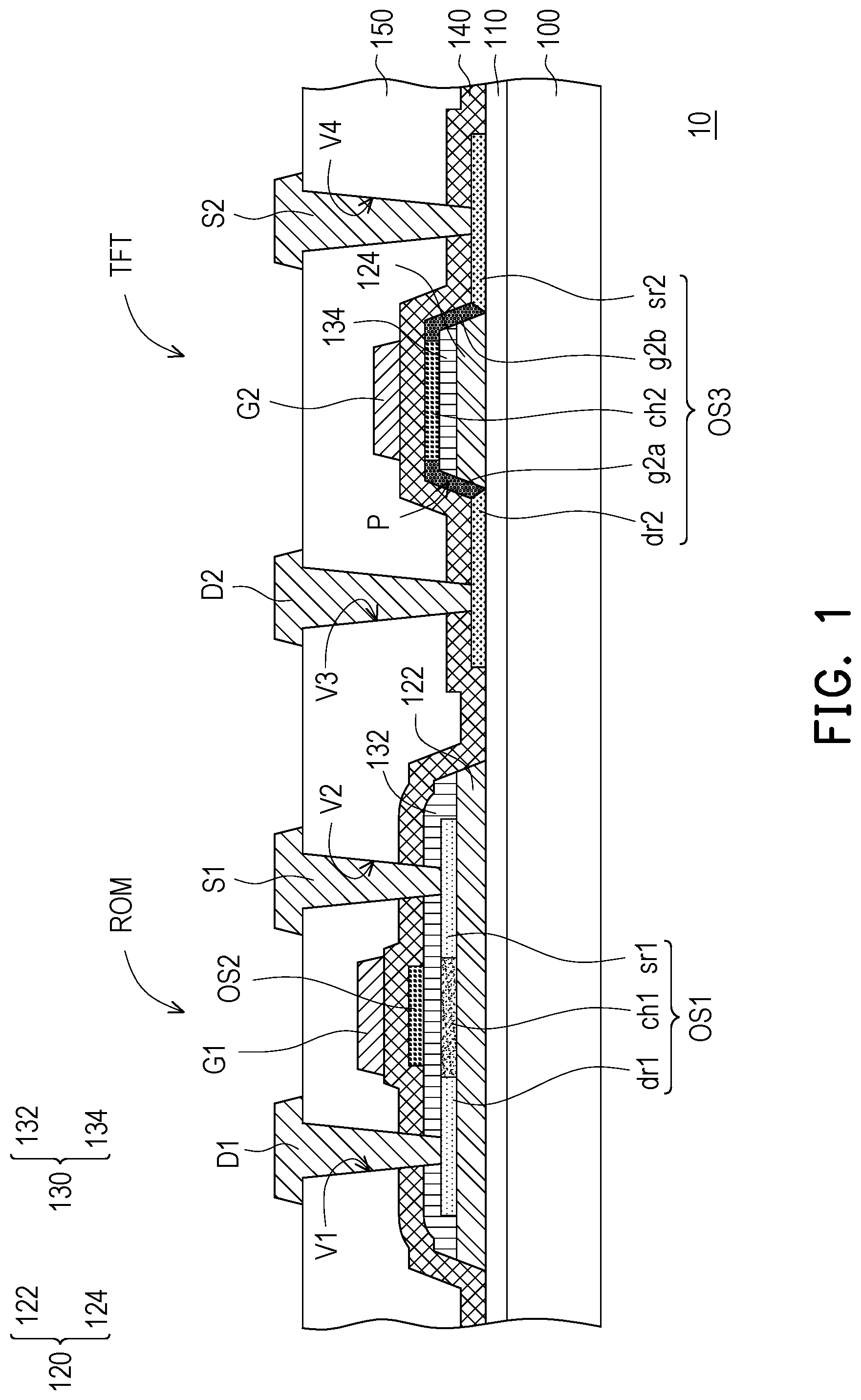
is a schematic cross-sectional view of a memory circuit according to an embodiment of the disclosure.
A is a circuit diagram of the memory circuit of .
B is a signal diagram of the memory circuit of A .
A to F are schematic cross-sectional views of a manufacturing method of the memory device of .
is a schematic cross-sectional view of a memory circuit according to an embodiment of the disclosure.
is a schematic cross-sectional view of a memory circuit according to an embodiment of the disclosure.
DESCRIPTION OF THE EMBODIMENTS
is a schematic cross-sectional view of a memory circuit according to an embodiment of the disclosure.
With reference to , a memory circuit 10 includes a substrate 100 , an oxide insulating layer 120 , a first gate dielectric layer 130 , a second gate dielectric layer 140 , a memory device ROM, and a thin film transistor TFT. In this embodiment, the memory circuit 10 further includes a buffer layer 110 and an interlayer dielectric layer 150 .
A material of the substrate 100 may be glass, quartz, an organic polymer, an opaque/reflective material (e.g., a conductive material, metal, a wafer, ceramics, or other suitable materials), or other suitable materials. If a conductive material or metal is used, an insulating layer (not shown) is used to cover the substrate 100 to avoid the short circuit problem. In some embodiments, the substrate 100 is a flexible substrate, and the material of the substrate 100 is, for example, polyethylene terephthalate (PET), polyethylene naphthalate (PEN), polyester (PES), polymethylmethacrylate (PMMA), polycarbonate (PC), polyimide (PI), metal foil, or other flexible materials.
In some embodiments, the buffer layer 110 is located above the substrate 100 , and the buffer layer 110 includes hydrogen. For instance, a material of the buffer layer 110 includes hydrogen-containing silicon nitride (or hydrogenated silicon nitride) or other suitable materials. In some embodiments, the buffer layer 110 blankets the substrate 100 . In some embodiments, a thickness of the buffer layer 110 is 100 angstroms to 6,000 angstroms.
The oxide insulating layer 120 is located above the substrate 100 . In this embodiment, the oxide insulating layer 120 is located on the buffer layer 110 . In some embodiments, the oxide insulating layer 120 is patterned so as not to cover a portion of the buffer layer 110 . In other words, the oxide insulating layer 120 covers a portion of the top surface of the buffer layer 110 and does not cover another portion of the top surface of the buffer layer 110 . In some embodiments, the oxide insulating layer 120 includes a first oxygen-containing structure 122 and a second oxygen-containing structure 124 . In some embodiments, the first oxygen-containing structure 122 and the second oxygen-containing structure 124 are separated from each other. In some embodiments, a material of the oxide insulating layer 120 includes silicon oxide, silicon oxynitride, aluminum oxide, hafnium oxide, or other suitable materials. In some embodiments, a thickness of the oxide insulating layer 120 is 300 angstroms to 5,000 angstroms.
The memory device ROM and the thin film transistor TFT are located above the substrate 100 . In some embodiments, the memory device ROM and the thin film transistor TFT are located on the oxide insulating layer 120 . The memory device ROM includes a first metal oxide layer OS 1 , a second metal oxide layer OS 2 , a first gate G 1 , a first source S 1 , and a first drain D 1 . The thin film transistor TFT includes a third metal oxide layer OS 3 , a second gate G 2 , a second source S 2 , and a second drain D 2 .
The first metal oxide layer OS 1 is located above the first oxygen-containing structure 122 of the oxide insulating layer 120 , and the first metal oxide layer OS 1 contacts a top surface of the first oxygen-containing structure 122 . The first oxygen-containing structure 122 is located between the first metal oxide layer OS 1 and the buffer layer 110 . The buffer layer 110 and the first oxygen-containing structure 122 are located between the first metal oxide layer OS 1 and the substrate 100 .
The first metal oxide layer OS 1 includes a first source region sr 1 , a first drain region dr 1 , and a first channel region ch 1 located between the first source region sr 1 and the first drain region dr 1 . A resistivity of the first source region sr 1 and a resistivity of the first drain region dr 1 are lower than a resistivity of the first channel region ch 1 . In some embodiments, a distance between the first channel region ch 1 and the substrate 100 is substantially equal to a distance between the first source region sr 1 and the substrate 100 and the distance between the first drain region dr 1 and the substrate 100 .
In some embodiments, the first oxygen-containing structure 122 under the first metal oxide layer OS 1 can supplement oxygen to the first metal oxide layer OS 1 , so that the resistivity of the first metal oxide layer OS 1 is increased. In this embodiment, the first source region sr 1 , the first drain region dr, and the first oxygen-containing structure 122 under the first channel region ch 1 have substantially uniform thicknesses.
The first gate dielectric layer 130 is located above the oxide insulating layer 120 and includes a first dielectric structure 132 and a second dielectric structure 134 . The first dielectric structure 132 of the first gate dielectric layer 130 is located on the first metal oxide layer OS 1 and covers the first metal oxide layer OS 1 . In some embodiments, the first source region sr 1 , the first drain region dr 1 , and the first channel region ch 1 are all located between the first oxygen-containing structure 122 of the oxide insulating layer 120 and the first dielectric structure 132 of the first gate dielectric layer 130 .
The second dielectric structure 134 is located above the second oxygen-containing structure 124 , and the second oxygen-containing structure 124 is located between the second dielectric structure 134 and the buffer layer 110 . The second oxygen-containing structure 124 and the second dielectric structure 134 are stacked on each other to form a protruding structure P. In some embodiments, a material of the first gate dielectric layer 130 includes silicon oxide, silicon oxynitride, aluminum oxide, hafnium oxide, or other suitable materials. In some embodiments, a thickness of the first gate dielectric layer 130 is 100 angstroms to 1,000 angstroms.
The second metal oxide layer OS 2 is located above the first dielectric structure 132 of the first gate dielectric layer 130 and overlaps the first channel region ch 1 of the first metal oxide layer OS 1 . The first dielectric structure 132 is located between the first metal oxide layer OS 1 and the second metal oxide layer OS 2 .
The third metal oxide layer OS 3 is located on the protruding structure P, covers the top surface and the side surface of the protruding structure P, and extends to the top surface of the buffer layer 110 . The third metal oxide layer OS 3 contacts the top surface of the second dielectric structure 134 , the side surface of the second dielectric structure 134 , the side surface of the second oxygen-containing structure 124 , and the top surface of the buffer layer 110 .
The third metal oxide layer OS 3 includes a second drain region dr 2 , a second source region sr 2 , a second channel region ch 2 , a resistance gradient region g 2 a connected between the second drain region dr 2 and the second channel region ch 2 , and a resistance gradient region g 2 b connected between the second source region sr 2 and the second channel region ch 2 . The second channel region ch 2 covers the top surface of the second dielectric structure 134 , and the protruding structure P is located between the buffer layer 110 and the second channel region ch 2 . The resistance gradient region g 2 a and the resistance gradient region g 2 b contact the side surfaces of the protruding structure P (including the side surface of the second dielectric structure 134 and the side surface of the second oxygen-containing structure 124 ). The second drain region dr 2 and the second source region sr 2 extend from the side surface of the protruding structure P in a direction away from the protruding structure P, and the second drain region dr 2 and the second source region sr 2 contact the top surface of the buffer layer 110 . A distance between the second channel region ch 2 and the substrate 100 is greater than a distance between the second drain region dr 2 and the substrate 100 and a distance between the second source region sr 2 and the substrate 100 .
In some embodiments, the protruding structure P under the third metal oxide layer OS 3 can supplement oxygen to the third metal oxide layer OS 3 , so that the resistivity of the third metal oxide layer OS 3 is increased. In this way, the thin film transistor TFT is prevented from being short-circuited because the resistivity of the second channel region ch 2 is excessively low. In addition, in some embodiments, the first dielectric structure 132 under the second metal oxide layer OS 2 also supplements oxygen to the second metal oxide layer OS 2 , so that the resistivity of the second metal oxide layer OS 2 is adjusted.
The overall thickness of the protruding structure P may affect its capability of supplementing oxygen to the third metal oxide layer OS 3 , so that the resistivity of the third metal oxide layer OS 3 in different regions is affected. To be specific, below the second channel region ch 2 , the overall thickness of the protruding structure P is relatively large, so the resistivity of the second channel region ch 2 is relatively large. Below the resistance gradient region g 2 a and the resistance gradient region g 2 b , the overall thickness of the protruding structure P gradually decreases, so the resistivity of the resistance gradient region g 2 a and resistivity the resistance gradient region g 2 b also gradually decrease. In other words, the resistivity of the resistance gradient region g 2 a and the resistivity of the resistance gradient region g 2 b decrease as distances from the second channel region ch 2 increase. There is no protruding structure P under the second drain region dr 2 and the second source region sr 2 , and the resistivity of the second drain region dr 2 and the resistivity of the second source region sr 2 are lower than those of the second channel region ch 2 , the resistance gradient region g 2 a , and the resistance gradient region g 2 b . In some embodiments, the oxygen concentration of the second channel region ch 2 is greater than the oxygen concentration of the resistance gradient region g 2 a and the oxygen concentration of the resistance gradient region g 2 b . The oxygen concentration of the resistance gradient region g 2 a and the oxygen concentration of the resistance gradient region g 2 b are greater than the oxygen concentration of the second drain region dr 2 and the oxygen concentration of the second source region sr 2 .
In some embodiments, the materials of the first metal oxide layer OS 1 , the second metal oxide layer OS 2 , and the third metal oxide layer OS 3 include metal compounds such as indium gallium tin zinc oxide (IGTZO) or indium gallium zinc oxide (IGZO), indium tin zinc oxide (ITZO), aluminum zinc tin oxide (AZTO), and indium tungsten zinc oxide (IWZO), or include oxides of any three of gallium (Ga), zinc (Zn), indium (In), tin (Sn), aluminum (Al), and tungsten (W), or lanthanide rare earth-doped metal oxides (e.g., Ln-IZO). In some embodiments, the first metal oxide layer OS 1 , the second metal oxide layer OS 2 , and the third metal oxide layer OS 3 include the same material. In other embodiments, the material of the first metal oxide layer OS 1 is different from the materials of the second metal oxide layer OS 2 and the third metal oxide layer OS 3 . In some embodiments, the second metal oxide layer OS 2 and the third metal oxide layer OS 3 belong to the same patterned layer. In some embodiments, the carrier mobility of the second metal oxide layer OS 2 and the carrier mobility of the second channel region ch 2 of the third metal oxide layer OS 3 are greater than the carrier mobility of the first channel region ch 1 of the first metal oxide layer OS 1 , thereby increasing the switching speed of the thin film transistor TFT.
The second gate dielectric layer 140 is located above the buffer layer 110 , the first dielectric structure 132 of the first gate dielectric layer 130 , the second metal oxide layer OS 2 , and the third metal oxide layer OS 3 . The second metal oxide layer OS 2 is located between the first dielectric structure 132 of the first gate dielectric layer 130 and the second gate dielectric layer 140 . The third metal oxide layer OS 3 is located between the second dielectric structure 134 of the first gate dielectric layer 130 and the second gate dielectric layer 140 and between the buffer layer 110 and the second gate dielectric layer 140 . In some embodiments, a material of the second gate dielectric layer 140 includes silicon oxide, silicon oxynitride, aluminum oxide, hafnium oxide, or other suitable materials. In some embodiments, a thickness of the second gate dielectric layer 140 is 500 angstroms to 2,000 angstroms. In some embodiments, the thickness of the first gate dielectric layer 140 is less than the thickness of the second gate dielectric layer 130 , thereby making it easier for electrons to tunnel from the first channel region ch 1 to the second metal oxide layer OS 2 , and the switching speed of the memory device ROM is thus improved.
The first gate G 1 and the second gate G 2 are located on the second gate dielectric layer 140 and respectively overlap the first channel region ch 1 of the first metal oxide layer OS 1 and the second channel region ch 2 of the third metal oxide layer OS 3 . The second gate dielectric layer 140 is located between the first gate G 1 and the second metal oxide layer OS 2 and between the second gate G 2 and the third metal oxide layer OS 3 . The second metal oxide layer OS 2 is located between the first gate G 1 and the first channel region ch 1 of the first metal oxide layer OS 1 .
In some embodiments, the materials of the first gate G 1 and the second gate G 2 may include metals, such as chromium (Cr), gold (Au), silver (Ag), copper (Cu), tin (Sn), lead (Pb), hafnium (Hf), tungsten (W), molybdenum (Mo), neodymium (Nd), titanium (Ti), tantalum (Ta), aluminum (Al), zinc (Zn), alloys of any combination of the foregoing metals, or stacks of the foregoing metals and/or alloys, but the disclosure is not limited thereto. The first gate G 1 and the second gate G 2 can also use other conductive materials, such as metal nitride, metal oxide, metal oxynitride, stacked layers of metal and other conductive materials, or other materials with conductive properties.
The interlayer dielectric layer 150 is located on the second gate dielectric layer 140 and covers the first gate G 1 and the second gate G 2 . In some embodiments, a material of the interlayer dielectric layer 150 includes silicon oxide, silicon nitride, silicon oxynitride, hafnium oxide, aluminum oxide, or other insulating materials.
A first contact hole V 1 and a second contact hole V 2 pass through the interlayer dielectric layer 150 , the second gate dielectric layer 140 , and the first dielectric structure 132 . The first drain D 1 and the first source S 1 are located on the interlayer dielectric layer 150 and are respectively filled in the first contact hole V 1 and the second contact hole V 2 to be electrically connected to the first metal oxide layer OS 1 . The first drain D 1 and the first source S 1 are respectively connected to the first drain region dr 1 and the first source region sr 1 of the first metal oxide layer OS 1 .
A third contact hole V 3 and a fourth contact hole V 4 pass through the interlayer dielectric layer 150 and the second gate dielectric layer 140 . The second drain D 2 and the second source S 2 are located on the interlayer dielectric layer 150 and are respectively filled in the third contact hole V 3 and the fourth contact hole V 4 to be electrically connected to the third metal oxide layer OS 3 . The second drain D 2 and the second source S 2 are respectively connected to the second drain region dr 2 and the second source region sr 2 of the third metal oxide layer OS 3 .
The materials of the first drain D 1 , the first source S 1 , the second drain D 2 , and the second source S 2 may include metals, such as chromium, gold, silver, copper, tin, lead, hafnium, tungsten, molybdenum, neodymium, titanium, tantalum, aluminum, zinc, alloys of any combination of the foregoing metals, or stacks of the foregoing metals and/or alloys, but the disclosure is not limited thereto. The first drain D 1 , the first source S 1 , the second drain D 2 , and the second source S 2 can also use other conductive materials, such as metal nitride, metal oxide, metal oxynitride, stacked layers of metal and other conductive materials, or other materials with conductive properties.
A is a circuit diagram of the memory circuit of . B is a signal diagram of the memory circuit of A . In B , the vertical axis is voltage, and the horizontal axis is time.
With reference to and A together, the memory circuit 10 further includes a word line WL, a bit line BL, a data line DL, and a source line SL. The word line WL is electrically connected to the second gate G 2 of the thin film transistor TFT. The bit line BL is electrically connected to the second drain D 2 of the thin film transistor TFT. The second source S 2 of the thin film transistor TFT is electrically connected to the first gate G 1 of the memory device ROM. The data line DL is electrically connected to the first drain D 1 of the memory device ROM. The source line SL is electrically connected to the first source S 1 of the memory device ROM.
With reference to , A , and B , when the write command of the memory device ROM is executed, a voltage is applied to the second gate G 2 of the thin film transistor TFT through the word line WL to turn on the thin film transistor TFT, and at the same time, a first voltage (e.g., 15 V to 30 V) is applied to the second drain D 2 of the thin film transistor TFT through the bit line BL. The signal on the bit line BL is transmitted to the first gate G 1 of the memory device ROM, and the electric field causes electrons to tunnel from the first metal oxide layer OS 1 through the first dielectric structure 132 of the first gate dielectric layer 130 into the second metal oxide layer OS 2 . Since electrons are stored in the second metal oxide layer OS 2 , the threshold voltage (V th ) of the memory device ROM is changed.
When the read command of the memory device ROM is executed, a voltage is applied to the second gate G 2 of the thin film transistor TFT through the word line WL to turn on the thin film transistor TFT, and at the same time, a second voltage (e.g., 5 V to 15 V) is applied to the second drain D 2 of the thin film transistor TFT through the bit line BL. The signal on the bit line BL is transmitted to the first gate G 1 of the memory device ROM to turn on the memory device ROM, and at the same time, a voltage is applied to the first drain D 1 of the memory device ROM through the data line DL, so that a voltage difference is generated between the first drain D 1 and the first source S 1 of the memory device ROM, so that the signal can pass through the memory device ROM. By reading the signal passing through the memory device ROM, it can be known that the memory device ROM is currently in state “1” or state “0”. The second voltage used when executing the read command is lower than the first voltage used when executing the write command, so the threshold voltage of the memory device ROM is not easily changed due to electron tunneling when executing the write command.
When the erase command of the memory device ROM is executed, a voltage is applied to the second gate G 2 of the thin film transistor TFT through the word line WL to turn on the thin film transistor TFT, and at the same time, a third voltage (e.g., −15 V to −30 V) is applied to the second drain D 2 of the thin film transistor TFT through the bit line BL. The signal on the bit line BL is transmitted to the first gate G 1 of the memory device ROM, and the electric field causes electrons to tunnel from the second metal oxide layer OS 2 through the first dielectric structure 132 of the first gate dielectric layer 130 into the first metal oxide layer OS 1 , so that the threshold voltage of the memory device ROM may return to the original value.
Based on the above, the memory device ROM provides the advantage of high access speed.
A to F are schematic cross-sectional views of a manufacturing method of the memory device of .
With reference to A , the buffer layer 110 and the oxide insulating layer 120 are formed on the substrate 100 . In some embodiments, the buffer layer 110 blankets the substrate 100 , and the oxide insulating layer 120 blankets the buffer layer 110 .
A first metal oxide layer OS 1 ′ is formed above the oxide insulating layer 120 . In some embodiments, the method of forming the first metal oxide layer OS 1 ′ includes the following steps. A first semiconductor material layer (not shown) is formed on the oxide insulating layer 120 . A patterned photoresist (not shown) is formed on the first semiconductor material layer. The first semiconductor material layer is etched to form the first metal oxide layer OS 1 ′ by treating the patterned photoresist as a mask. As a final step, the patterned photoresist is removed.
With reference to B , the first gate dielectric layer 130 is formed on the first metal oxide layer OS 1 ′ and the oxide insulating layer 120 . In some embodiments, the first gate dielectric layer 130 blankets the first metal oxide layer OS 1 ′ and the oxide insulating layer 120 .
With reference to C , a patterning process is performed on the oxide insulating layer 120 and the first gate dielectric layer 130 , such that the oxide insulating layer 120 includes a first oxygen-containing structure 122 and a second oxygen-containing structure 124 , and the first gate dielectric layer 130 includes a first dielectric structure 132 and a second dielectric structure 134 . The first metal oxide layer OS 1 ′ is located between the first oxygen-containing structure 122 and the first dielectric structure 132 . The second oxygen-containing structure 124 and the second dielectric structure 134 are stacked on each other to form a protruding structure P. In some embodiments, the patterning process includes wet etching or dry etching, and the patterning process etching stops at the buffer layer 110 .
In some embodiments, the oxide insulating layer 120 and the first gate dielectric layer 130 are patterned by the same mask, so that the side surface of the first oxygen-containing structure 122 is aligned with the first dielectric structure 132 , and the side surface of the second oxygen-containing structure 124 is aligned with the second dielectric structure 134 .
Next, with reference to D , the second metal oxide layer OS 2 and a third metal oxide layer OS 3 ′ are formed on the first gate dielectric layer 130 . In this embodiment, the second metal oxide layer OS 2 is formed on the first dielectric structure 132 of the first gate dielectric layer 130 , and the third metal oxide layer OS 3 ′ is formed on the top surface of the protruding structure P, the side surface of the protruding structure P, and the buffer layer 110 . In some embodiments, the method of forming the second metal oxide layer OS 2 and the third metal oxide layer OS 3 ′ includes the following steps. A second semiconductor material layer (not shown) is formed on the buffer layer 110 , the oxide insulating layer 120 , and the first gate dielectric layer 130 . A patterned photoresist (not shown) is formed on the second semiconductor material layer. The second semiconductor material layer is etched to form the second metal oxide layer OS 2 and the third metal oxide layer OS 3 ′ by treating the patterned photoresist as a mask. As a final step, the patterned photoresist is removed. In this embodiment, since the first metal oxide layer OS 1 ′ is covered by the first oxygen-containing structure 122 and the first dielectric structure 132 , the foregoing etching process may not cause damage to the first metal oxide layer OS 1 ′.
With reference to E , the second gate dielectric layer 140 is formed on the second metal oxide layer OS 2 and the third metal oxide layer OS 3 ′. In this embodiment, the second gate dielectric layer 140 is located on the second metal oxide layer OS 2 , the first dielectric structure 132 , the buffer layer 110 , and the third metal oxide layer OS 3 ′.
The first gate G 1 and the second gate G 2 are formed above the second gate dielectric layer 140 . The second metal oxide layer OS 2 is located between the first gate G 1 and the first metal oxide layer OS 1 ′, and the second gate G 2 overlaps the third metal oxide layer OS 3 ′.
In some embodiments, before the first gate G 1 and the second gate G 2 are formed, a heat treatment process is performed to diffuse oxygen in the protruding structure P into the third metal oxide layer OS 3 ′, thereby increasing the resistivity of the third metal oxide layer OS 3 ′ on the protruding structure P. In some embodiments, in the heat treatment process, oxygen in the first dielectric structure 132 is further diffused into the second metal oxide layer OS 2 , thereby increasing the resistivity of the second metal oxide layer OS 2 . In some embodiment, the heat treatment process is, for example, a heating process when the second gate dielectric layer 140 is deposited, but the disclosure is not limited thereto.
Next, a doping process DP is performed on the first metal oxide layer OS 1 ′ and the third metal oxide layer OS 3 ′ by treating the first gate G 1 and the second gate G 2 as masks. In this way, the first metal oxide layer OS 1 including the first source region sr 1 , the first drain region dr 1 , and the first channel region ch 1 and the third metal oxide layer OS 3 including the second source region sr 2 , the second drain region dr 2 , the resistance gradient region g 2 a , the resistance gradient region g 2 b , and the second channel region ch 2 are formed. In some embodiments, the doping process DP is, for example, a hydrogen plasma process or other suitable processes. In some embodiments, the first gate G 1 completely shields the second metal oxide layer OS 2 in a normal direction ND of the top surface of the substrate 100 . Therefore, the first source region sr 1 and the first drain region dr 1 are not shielded by the second metal oxide layer OS 2 during the doping process DP.
In some embodiments, the buffer layer 110 provides hydrogen to the third metal oxide layer OS 3 during the process, thereby reducing the resistivity of the second source region sr 2 and the resistivity of the second drain region dr 2 .
In this embodiment, the first gate G 1 and the second gate G 2 belong to the same patterned layer, and the first metal oxide layer OS 1 and the second metal oxide layer OS 2 may be doped through the same doping process DP. Therefore, the manufacturing costs of the memory device and the thin film transistor may be saved.
With reference to F , the interlayer dielectric layer 150 is formed on the second gate dielectric layer 140 . Next, an etching process is performed to form the first contact hole V 1 , the second contact hole V 2 , the third contact hole V 3 , and the fourth contact hole V 4 .
Last but not least, with reference to again, the first drain D 1 , the first source S 1 , the second drain D 2 , and the second source S 2 are formed on the interlayer dielectric layer 150 and are respectively filled in the first contact hole V 1 , the second contact hole V 2 , the third contact hole V 3 , and the fourth contact hole V 4 . The memory circuit 10 is substantially completed so far. In some embodiments, the method of forming the first source S 1 , the first drain D 1 , the second source S 2 , and the second drain D 2 includes the following steps. A conductive material layer (not shown) is formed on the interlayer dielectric layer 150 . A patterned photoresist (not shown) is formed on the conductive material layer. The conductive material layer is etched to form the first source S 1 , the first drain D 1 , the second source S 2 , and the second drain D 2 by treating the patterned photoresist as a mask. As a final step, the patterned photoresist is removed. In other words, the first source S 1 , the first drain D 1 , the second source S 2 , and the second drain D 2 belong to the same patterned layer.
is a schematic cross-sectional view of a memory circuit according to an embodiment of the disclosure. It should be noted that the reference numerals and a part of the contents in the embodiment of are also used to describe the embodiment of , in which the same reference numerals are used to represent identical or similar elements, and thus descriptions of the same technical contents are omitted. Please refer to the descriptions of the previous embodiments for the omitted part, which will not be repeated hereinafter.
The main differences between a memory circuit 20 of and the memory circuit 10 of is that the thin film transistor TFT of the memory circuit 20 further includes a bottom gate BG.
With reference to A , the bottom gate BG is located on the substrate 100 . The buffer layer 110 is located on the bottom gate BG. The third metal oxide layer OS 3 is located between the bottom gate BG and the second gate G 2 , and the protruding structure P is located between the bottom gate BG and the third metal oxide layer OS 3 . In some embodiments, a length L 2 of the bottom gate BG is greater than a length L 1 of the second gate G 2 .
is a schematic cross-sectional view of a memory circuit according to an embodiment of the disclosure. It should be noted that the reference numerals and a part of the contents in the embodiment of are also used to describe the embodiment of , in which the same reference numerals are used to represent identical or similar elements, and thus descriptions of the same technical contents are omitted. Please refer to the descriptions of the previous embodiments for the omitted part, which will not be repeated hereinafter.
The main differences between a memory circuit 30 of and the memory circuit 10 of is that the first metal oxide layer OS 1 of the memory device ROM of the memory circuit 30 includes a resistance gradient region g 1 a and a resistance gradient region g 1 b . The resistance gradient region g 1 a is connected between the first drain region dr 1 and the first channel region ch 1 , and the resistance gradient region g 1 b is connected between the first source region sr 1 and the first channel region ch 1 .
With reference to , the first channel region ch 1 of the first metal oxide layer OS 1 is located on the first oxygen-containing structure 122 , and the first oxygen-containing structure 122 is located between the first channel region ch 1 and the buffer layer 110 . The resistance gradient region g 1 a and the second resistance gradient region g 1 b of the first metal oxide layer OS 1 contact the side surface of the first oxygen-containing structure 122 . The first drain region dr 1 and the first source region sr 1 extend from the side surface of the first oxygen-containing structure 122 in a direction away from the first oxygen-containing structure 122 , and the first drain region dr 1 and the first source region sr 1 contact the top surface of the buffer layer 110 . A distance between the first channel region ch 1 and the substrate 100 is greater than a distance between the first drain region dr 1 and the substrate 100 and a distance between the first source region sr 1 and the substrate 100 .
In some embodiments, the first oxygen-containing structure 122 under the first metal oxide layer OS 1 can supplement oxygen to the first metal oxide layer OS 1 , so that the resistivity of the first metal oxide layer OS 1 is increased. In this way, the memory device ROM is prevented from being short-circuited because the resistivity of the first channel region ch 1 is excessively low.
The thickness of the first oxygen-containing structure 122 may affect its capability of supplementing oxygen to the first metal oxide layer OS 1 , so that the resistivity of the first metal oxide layer OS 1 in different regions is affected. To be specific, below the first channel region ch 1 , the overall thickness of the first oxygen-containing structure 122 is relatively large, so the resistivity of the first channel region ch 1 is relatively large. Below the resistance gradient region g 1 a and the resistance gradient region g 1 b , the thickness of the first oxygen-containing structure 122 gradually decreases, so the resistivity of the resistance gradient region g 1 a and resistivity the resistance gradient region g 1 b also decrease gradually. In other words, the resistivity of the resistance gradient region g 1 and the resistivity of the resistance gradient region g 1 b decrease as distances from the first channel region ch 1 increase. There is no first oxygen-containing structure 122 under the first drain region dr 1 and the first source region sr 1 , and the resistivity of the first drain region dr 1 and the resistivity of the first source region sr 1 are lower than those of the first channel region ch 1 , the resistance gradient region g 1 a , and the resistance gradient region g 1 b . In some embodiments, the oxygen concentration of the first channel region ch 1 is greater than the oxygen concentration of the resistance gradient region g 1 a and the oxygen concentration of the resistance gradient region g 1 b . The oxygen concentration of the resistance gradient region g 1 a and the oxygen concentration of the resistance gradient region g 1 b are greater than the oxygen concentration of the first drain region dr 1 and the oxygen concentration of the first source region sr 1 .
In some embodiments, the buffer layer 110 provides hydrogen to the first metal oxide layer OS 1 during the process, thereby reducing the resistivity of the first source region sr 1 and the resistivity of the first drain region dr 1 .
In view of the above, in the memory device ROM provided by the disclosure, the second metal oxide layer OS 2 is located between the first gate G 1 and the first metal oxide layer OS 1 . By applying a voltage to the first gate G 1 , electrons may tunnel between the first metal oxide layer OS 1 and the second metal oxide layer OS 2 , so that the memory device ROM may be switched rapidly.
It will be apparent to those skilled in the art that various modifications and variations can be made to the disclosed embodiments without departing from the scope or spirit of the disclosure. In view of the foregoing, it is intended that the disclosure covers modifications and variations provided that they fall within the scope of the following claims and their equivalents.
Figures (9)
Citations
This patent cites (6)
- US11227875
- US12015066
- US2021/0036028
- US2021/0273112
- US206758441
- US112310151