Abstract
A signal processing device, used to suppress cross-talk nonlinear distortion of a RF front end circuit. The first circuit generates a first PD signal and a second PD signal according to a first input signal and a second input signal. The first PD signal and the second PD signal are provided to a first PA and a second PA of the RF front end circuit. The second circuit generates a first control signal and a second control signal according to a first output signal, a second output signal, a first DPD signal and a second DPD signal, so as to control the first circuit to generate the first PD signal and the second PD signal. The first PA generates the first output signal through a first filter having a first operating BW. The second PA generates the second output signal through a second filter having a second operating BW.
Claims (16)
1. A signal processing device, for suppressing a crosstalk nonlinear distortion of a radio frequency (RF) front end circuit, the RF front end circuit comprises a first power amplifier (PA), a second PA, a first filter and a second filter, the signal processing device comprising: a first circuit, configured to receive a first input signal through a first input transmission path, receive a second input signal through a second input transmission path, generate a first pre-distortion (PD) signal and a second PD signal according to the first input signal and the second input signal, transmit the first PD signal to the first PA through the first input transmission path, and transmit the second PD signal to the second PA through the second input transmission path, wherein the first input signal has a first input bandwidth (BW), and the second input signal has a second input BW; and a second circuit, configured to receive a first output signal through a first output feedback path, receive a second output signal through a second output feedback path, receive a first digital-pre-distortion (DPD) signal through a first feedback path, receive a second DPD signal through a second feedback path, generate a first control signal and a second control signal according to the first output signal, the second output signal, the first DPD signal and the second DPD signal, and control the first circuit to generate the first PD signal and the second PD signal according to the first control signal and the second control signal, wherein, the first PA generates the first output signal through the first filter, the first filter has a first operating BW corresponding to the first input BW, and the second PA generates the second output signal through the second filter, the second filter has a second operating BW corresponding to the second input BW.
Show 15 dependent claims
2. The signal processing device according to claim 1 , wherein the first input BW is not equal to the second input BW, the first operating BW is greater than or equal to twice of the first input BW, the second operating BW is greater than or equal to twice of the second input BW.
3. The signal processing device according to claim 1 , wherein the first feedback path is connected to the first input transmission path, and the second feedback path is connected to the second input transmission path.
4. The signal processing device according to claim 1 , wherein the first PD signal is coupled to the second PD signal on the second input transmission path, the first PD signal has a first coupling gain, and the second PD signal is coupled to the first PD signal on the first input transmission path, the second PD signal has a second coupling gain.
5. The signal processing device according to claim 1 , wherein the first circuit comprising: a first PD circuit, configured to receive the first input signal through the first input transmission path, receive the second input signal through the second input transmission path, generate the first DPD signal according to the first input signal, the second input signal and the first control signal, and transmit the first DPD signal to the second circuit through the first feedback path; and a first digital-to-analog (D-A) converter and a first modulation and up-conversion (MUC) circuit, configured to convert the first DPD signal into the first PD signal, wherein, the first PD circuit, the first D-A converter and the first MUC circuit are disposed on the first input transmission path.
6. The signal processing device according to claim 5 , wherein the first PD circuit performs a coupling DPD (CP-DPD) process according to the first input signal, the second input signal and the first control signal.
7. The signal processing device according to claim 5 , wherein the second circuit comprises: a first analog-to-digital (A-D) converter and a first demodulation and down-conversion (DMDC) circuit, configured to generate a first intermediate signal according to the first output signal and the second output signal; and a first computing circuit, configured to generate the first control signal according to the first intermediate signal and the first DPD signal, wherein, the first computing circuit, the first A-D converter and the first DMDC circuit are disposed on the first output feedback path.
8. The signal processing device according to claim 7 , wherein the first A-D converter has a first sampling frequency, and the first sampling frequency is greater than or equal to twice of the first input BW.
9. The signal processing device according to claim 7 , wherein the first computing circuit performs a multi-input and multi-output (MIMO) indirect learning algorithm according to the first intermediate signal and the first DPD signal.
10. The signal processing device according to claim 9 , wherein the first computing circuit performs a least square (LS) operation to generate the first control signal, and adjusts filter-coefficients of the first PD circuit according to the first control signal.
11. The signal processing device according to claim 1 , wherein the first circuit comprising: a second PD circuit, configured to receive the first input signal through the first input transmission path, receive the second input signal through the second input transmission path, generate the second DPD signal according to the first input signal, the second input signal and the second control signal, and transmit the second DPD signal to the second circuit through the second feedback path; and a second digital-to-analog (D-A) converter and a second modulation and up-conversion (MUC) circuit, configured to convert the second DPD signal into the second PD signal, wherein, the second PD circuit, the second D-A converter and the second MUC circuit are disposed on the second input transmission path.
12. The signal processing device according to claim 11 , wherein the second PD circuit performs a coupling DPD (CP-DPD) process according to the first input signal, the second input signal and the second control signal.
13. The signal processing device according to claim 11 , wherein the second circuit comprises: a second analog-to-digital (A-D) converter and a second first demodulation and down-conversion (DMDC) circuit, configured to generate a second intermediate signal according to the first output signal and the second output signal; and a second computing circuit, configured to generate the second control signal according to the second intermediate signal and the second DPD signal, wherein, the second computing circuit, the second A-D converter and the second DMDC circuit are disposed on the second output feedback path.
14. The signal processing device according to claim 13 , wherein the second A-D converter has a second sampling frequency, and the second sampling frequency is greater than or equal to twice of the second input BW.
15. The signal processing device according to claim 13 , wherein the second computing circuit performs a multi-input and multi-output (MIMO) indirect learning algorithm according to the second intermediate signal and the second DPD signal.
16. The signal processing device according to claim 15 , wherein the second computing circuit performs a least square (LS) operation to generate the second control signal, and adjusts filter-coefficients of the second PD circuit according to the second control signal.
Full Description
Show full text →
This application claims the benefit of Taiwan application Serial No. 111138438, filed Oct. 11, 2022, the subject matter of which is incorporated herein by reference.
TECHNICAL FIELD
The present disclosure relates to an electronic device, and more particularly, relates to a signal processing device for suppressing crosstalk nonlinear distortion.
BACKGROUND
With the evolution of communication technology, the wireless communication system often employs a multi-input and multi-output (MIMO) multi-antenna architecture, and the radio frequency (RF) front-end circuit of the MIMO system has multiple RF components, such as the power amplifier (PA). When a plurality of RF components are densely disposed on a chip with a small area, a crosstalk effect will occur between the RF components. This crosstalk effect will then complicate the nonlinear distortion of the PAs, which is referred to as “crosstalk nonlinear distortion”.
In addition, in a MIMO system, the signals of each transmission path have different center frequencies, signal bandwidths (BW) or sampling frequencies. The above-mentioned crosstalk nonlinear distortion effect will greatly increase the BW of the coupled signal, which may increase the overall BW of the MIMO system by several times. In response to the increased bandwidth, the complexity of circuit design and the computation amounts of the system will be greatly increased, and circuitry components with higher hardware specifications must be provided. For example, high-speed (i.e., high sampling frequency) analog-to-digital (A-D) converters and digital-to-analog (D-A) converters must be provided.
Therefore, those skilled in the art are devoted to improve the signal processing of the MIMO system, so as to reduce the crosstalk nonlinear distortion of the RF components in the RF front end circuit.
SUMMARY
According to an aspect of the present disclosure, a signal processing device is provided for suppressing a crosstalk nonlinear distortion of a radio frequency (RF) front end circuit. The RF front end circuit comprises a first power amplifier (PA), a second PA, a first filter and a second filter. The signal processing device comprises a first circuit and a second circuit. The first circuit is configured to receive a first input signal through a first input transmission path, receive a second input signal through a second input transmission path, generate a first pre-distortion (PD) signal and a second PD signal according to the first input signal and the second input signal, transmit the first PD signal to the first PA through the first input transmission path, and transmit the second PD signal to the second PA through the second input transmission path, wherein the first input signal has a first input bandwidth (BW), and the second input signal has a second input BW. The second circuit is configured to receive a first output signal through a first output feedback path, receive a second output signal through a second output feedback path, receive a first digital-pre-distortion (DPD) signal through a first feedback path, receive a second DPD signal through a second feedback path, generate a first control signal and a second control signal according to the first output signal, the second output signal, the first DPD signal and the second DPD signal, and control the first circuit to generate the first PD signal and the second PD signal according to the first control signal and the second control signal. The first PA generates the first output signal through the first filter, the first filter has a first operating BW corresponding to the first input BW, and the second PA generates the second output signal through the second filter, the second filter has a second operating BW corresponding to the second input BW.
BRIEF DESCRIPTION OF THE DRAWINGS
A is a schematic diagram of a signal processing device according to an embodiment of the disclosure, which is applied to a communication system.
B is a schematic diagram of the signal processing device 1000 b according to another embodiment of the disclosure, which is applied to the communication system.
C is a schematic diagram of the signal processing device 1000 c according to still another embodiment of the disclosure, which is applied to the communication system.
A and 2 B are schematic diagrams showing operation of the signal processing device of A .
A is a schematic diagram of a signal processing device of a comparative example applied to a communication system.
B is a schematic diagram of the signal processing device of another comparative example applied to the communication system.
A is a schematic diagram of a signal processing device according to yet another embodiment of the disclosure, which is applied to a communication system.
B is a block diagram of the second circuit of the signal processing device of A .
In the following detailed description, for purposes of explanation, numerous specific details are set forth in order to provide a thorough understanding of the disclosed embodiments. It will be apparent, however, that one or more embodiments may be practiced without these specific details. In other instances, well-known structures and devices are schematically illustrated in order to simplify the drawing.
DETAILED DESCRIPTION
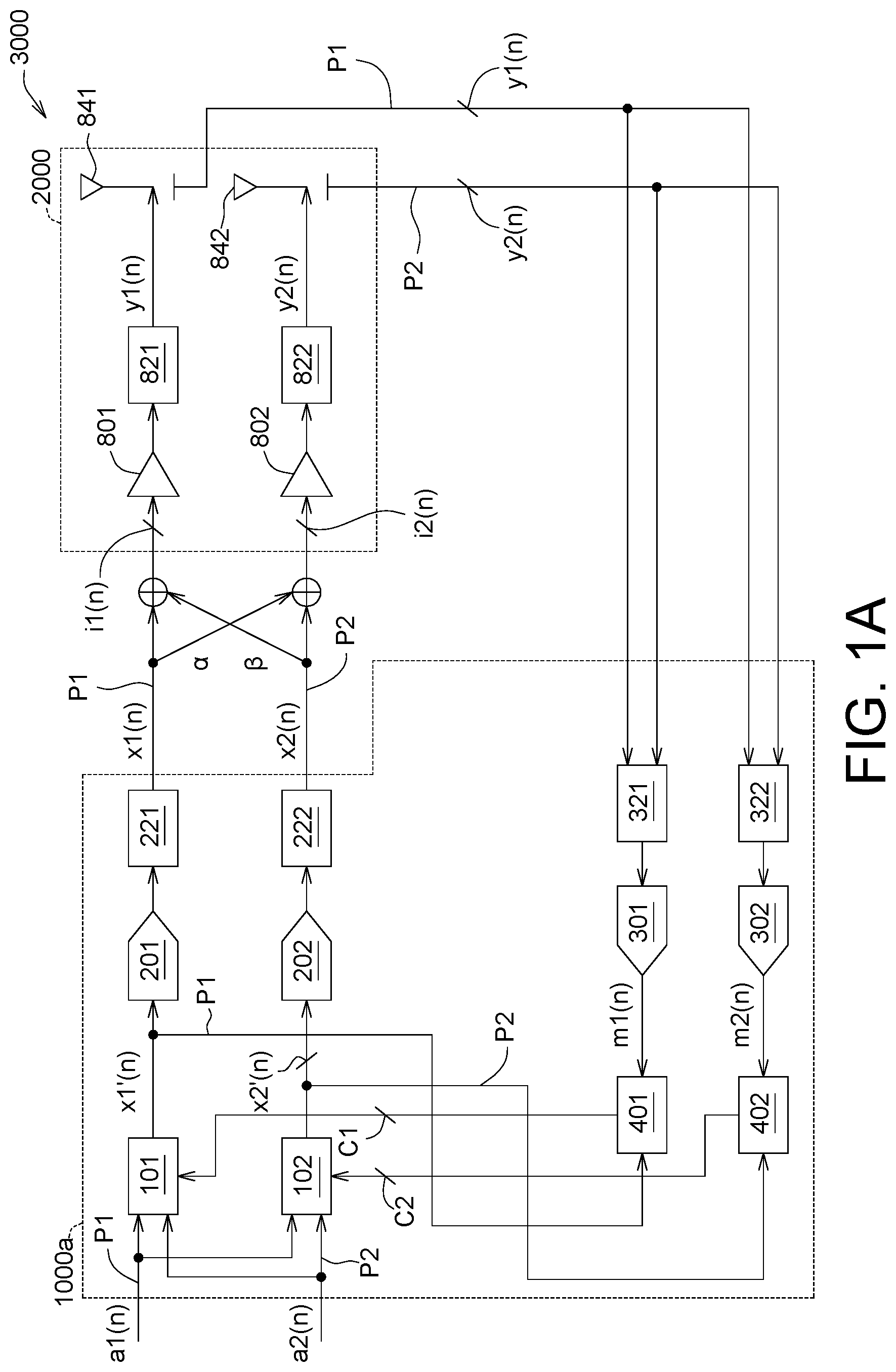
A is a schematic diagram of a signal processing device 1000 a according to an embodiment of the disclosure, which is applied to a communication system 3000 . As shown in A , the communication system 3000 includes an RF front end circuit 2000 . The signal processing device 1000 a is coupled to the RF front end circuit 2000 , and the signal processing device 1000 a is used to process nonlinear distortion of the RF front end circuit 2000 . The communication system 3000 is a multi-input and multi-output (MIMO) system. For example, the communication system 3000 has two inputs and two outputs. The signals of the communication system 3000 are respectively transmitted on the first path P 1 and the second path P 2 . The signal transmitted on the first path P 1 may be coupled to the second path P 2 , and similarly, the signal transmitted on the second path P 2 may be coupled to the first path P 1 . Therefore, nonlinear distortion of the RF front end circuit 2000 will be complicated, which is referred to as “crosstalk nonlinear distortion”.
The RF front end circuit 2000 includes a first power amplifier (PA) 801 , a second PA 802 , a first filter 821 , a second filter 822 , a first antenna 841 and a second antenna 842 . The first PA 801 , the first filter 821 and the first antenna 841 are disposed on the first path P 1 , and the second PA 802 , the second filter 822 and the second antenna 842 are disposed on the second path P 2 . On the first path P 1 of the RF front end circuit 2000 , the first PA 801 generates the first output signal y 1 ( n ) through the first filter 821 , and the nonlinear distortion caused by the first PA 801 occurs in an output signal y 1 ( n ). n). On the second path P 2 of the RF front end circuit 2000 , the second PA 802 generates the second output signal y 2 ( n ) through the second filter 822 , and the nonlinear distortion caused by the second PA 802 occurs in the second output signal y 2 ( n ). Since the signals transmitted by the first path P 1 and the second path P 2 are coupled to each other, the nonlinear distortion of the first output signal y 1 ( n ) and the second output signal y 2 ( n ) will be complicated and leads to a crosstalk nonlinear distortion.
The signal processing device 1000 a performs a pre-distortion (PD) process to generate a first PD signal x 1 ( n ) and a second PD signal x 2 ( n ), thereby reducing or suppressing the crosstalk nonlinear distortion of the first output signal y 1 ( n ) and the second output signal y 2 ( n ). The first PD signal x 1 ( n ) is transmitted to the first PA 801 through the first path P 1 , and the second PD signal x 2 ( n ) is transmitted to the second PA 802 through the second path P 2 . More specifically, the signal processing device 1000 a of the present embodiment receives the first input signal a 1 ( n ) and the second input signal a 2 ( n ) generated by the pre-stage circuit (not shown in A ) of the communication system 3000 , and the signal processing device 1000 a also receives the first output signal y 1 ( n ) and the second output signal y 2 ( n ) generated by the RF front end circuit 2000 . The signal processing device 1000 a performs pre-distortion processing (PD processing) according to the above-mentioned signals to generate a first PD signal x 1 ( n ) and a second PD signal x 2 ( n ). In addition, the first PD signal x 1 ( n ) and the second PD signal x 2 ( n ) are fed back and inputted to the signal processing device 1000 a.
The first input signal a 1 ( n ), the first PD signal x 1 ( n ) and the first output signal y 1 ( n ) are transmitted on the first path P 1 , the second input signal a 2 ( n ), the second PD signal x 2 ( n ) and the second output signal y 2 ( n ) are transmitted on the second path P 2 . Moreover, the first PD signal x 1 ( n ) and the second PD signal x 2 ( n ) are coupled to each other. For example, the first PD signal x 1 ( n ) is coupled to the second PD signal x 2 ( n ) in the second path P 2 , and the first PD signal x 1 ( n ) has a first coupling gain α. That is, the first PD signal x 1 ( n ) is attenuated by the first coupling gain α and then coupled to the second PD signal x 2 ( n ) to form the input signal i 2 ( n ) of the second PA 802 , as shown in equation (1): i 2( n )= x 2( n )+α* x 1( n ) equation (1)
Similarly, the second PD signal x 2 ( n ) is coupled to the first PD signal x 1 ( n ) on the first path P 1 , and the second PD signal x 2 ( n ) has a second coupling gain ß. That is, the second PD signal x 2 ( n ) is attenuated by the second coupling gain ß and then coupled to the first PD signal x 1 ( n ) to form the input signal i 1 ( n ) of the first PA 801 , as shown in equation (2): i 1( n )= x 1( n )+ß* x 2( n ) equation (2)
The first coupling gain α may be equal to or different from the second coupling gain ß. In this embodiment, the first coupling gain α is equal to the second coupling gain ß, and both the first coupling gain α and the second coupling gain ß are in the range of −12 dB to −20 dB.
The main components of the signal processing device 1000 a are: a first PD circuit 101 , a second PD circuit 102 , a first computing circuit 401 and a second computing circuit 402 . The first PD circuit 101 and the first computing circuit 401 are disposed on the first path P 1 , and the second PD circuit 102 and the second computing circuit 402 are disposed on the second path P 2 .
On the first path P 1 , the components related to the first PD circuit 101 are: the digital-to-analog (D-A) converter 201 and the modulation and up-conversion (MUC) circuit 221 . The first PD circuit 101 , the D-A converter 201 and the MUC circuit 221 are connected in series. The first PD circuit 101 performs digital pre-distortion (DPD) processing according to the first input signal a 1 ( n ) transmitted by the first path P 1 and the second input signal a 2 ( n ) transmitted by the second path P 2 , so as to generate a first DPD signal x 1 ′( n ). That is, the first PD circuit 101 performs pre-distortion processing according to signals of multiple paths, which may be referred to as “coupling digital pre-distortion (CP-DPD)”. The first PD circuit 101 is, for example, an adaptive filter, and adjusts filter-coefficients of the first PD circuit 101 according to the first control signal C 1 . Then, the D-A converter 201 performs conversion from the digital domain to the analog domain, and the MUC circuit 221 performs modulation and up-conversion to convert the first DPD signal x 1 ( n ) into a first PD signal x 1 ( n ).
On the other hand, on the first path P 1 , the components related to the first computing circuit 401 are: the analog-to-digital (A-D) converter 301 and the demodulation and down-conversion (DMDC) circuit 321 . The A-D converter 301 performs the conversion from the analog domain to the digital domain, and the DMDC circuit 321 performs DMDC operation to convert the first output signal y 1 ( n ) and the second output signal y 2 ( n ) into the first intermediate signal m 1 ( n ). The first computing circuit 401 generates a first control signal C 1 according to the first intermediate signal m 1 ( n ) and the first DPD signal x 1 ′( n ), so as to adjust the filter-coefficients of the first PD circuit 101 accordingly. In one example, the first computing circuit 401 performs a least square (LS) operation to generate the first control signal C 1 .
Similarly, on the second path P 2 , the components related to the second PD circuit 102 are: the D-A converter 202 and the MUC circuit 222 , which are connected to the second PD circuit 102 in series. The second PD circuit 102 performs “CP-DPD” processing according to the first input signal a 1 ( n ) transmitted by the first path P 1 and the second input signal a 2 ( n ) transmitted by the second path P 2 , so as to generate a second DPD signal x 2 ′( n ). Then, the D-A converter 202 and the MUC circuit 222 convert the second DPD signal x 2 ′( n ) into an up-converted second PD signal x 2 ( n ) in analog domain.
On the other hand, on the second path P 2 , the components related to the second computing circuit 402 are: the A-D converter 302 and the DMDC circuit 322 . The A-D converter 302 and the DMDC circuit 322 convert the first output signal y 1 ( n ) and the second output signal y 2 ( n ) into a second intermediate signal m 2 ( n ). The second computing circuit 402 performs operation (e.g., LS operation) according to the second intermediate signal m 2 ( n ) and the second DPD signal x 2 ′( n ), so as to generate a second control signal C 2 , and then to adjust filter-coefficients for the second PD circuit 102 .
B is a schematic diagram of the signal processing device 1000 b according to another embodiment of the disclosure, which is applied to the communication system 3000 . The signal processing device 1000 b of this embodiment is similar to the signal processing device 1000 a of A , the difference is that, the signal processing device 1000 b of this embodiment does not include the D-A converter 201 , the MUC circuit 221 , and the D-A converter 202 and the MUC circuit 222 . That is, in the embodiment of B , the D-A converter 201 , the MUC circuit 221 , the D-A converter 202 and the MUC circuit 222 may be existing components of the communication system 3000 .
The signal processing device 1000 b of this embodiment directly outputs the first DPD signal x 1 ′( n ) and the second DPD signal x 2 ′( n ). Then, the first DPD signal x 1 ′( n ) and the second DPD signal x 2 ′( n ) are performed by D-A conversion and up-conversion to form the first PD signal x 1 ( n ) and the second PD signal x 2 ( n ), which are then provided to the RF front end circuit 2000 .
C is a schematic diagram of the signal processing device 1000 c according to still another embodiment of the disclosure, which is applied to the communication system 3000 . The signal processing device 1000 c of this embodiment is similar to the signal processing device 1000 b of B , except that, the signal processing device 1000 c of this embodiment does not include the A-D converter 301 , the DMDC circuit 321 , and the A-D converter 302 and the DMDC circuit 322 . That is, in the embodiment of C , the A-D converter 301 , the DMDC circuit 321 , and the A-D converter 302 and the DMDC circuit 322 may be existing components of the communication system 3000 . The first intermediate signal m 1 ( n ) and the second intermediate signal m 2 ( n ) are generated by the communication system 3000 . The signal processing device 1000 c receives the first intermediate signal m 1 ( n ) and the second intermediate signal m 2 ( n ) from the communication system 3000 , and receives the first input signal a 1 ( n ) and the second input signal a 2 ( n ) from the pre-stage circuit, and then performs “CP-DPD” processing according to the above-mentioned signals to generate the first DPD signal x 1 ′( n ) and the second DPD signal x 2 ′( n ).
A and 2 B are schematic diagrams showing operation of the signal processing device 1000 a of A . Referring first to A , the first input signal a 1 ( n ) received through the first path P 1 is a baseband signal, and the first input signal a 1 ( n ) has a first input bandwidth Wi 1 . Moreover, the second input signal a 2 ( n ) received through the second path P 2 is also a baseband signal, and the second input signal a 2 ( n ) has a second input bandwidth Wi 2 . The first input bandwidth Wi 1 may be equal to or different from the second input bandwidth Wi 2 . In this embodiment, the first input bandwidth Wi 1 is different from the second input bandwidth Wi 2 , the first input bandwidth Wi 1 is, for example, 500 MHz, and the second input bandwidth Wi 2 is, for example, 1 GHz. That is, the second input bandwidth Wi 2 is substantially twice the first input bandwidth Wi 1 .
The first filter 821 and the second filter 822 are band pass filters (BPF), the first filter 821 has a first operating bandwidth W 1 , and the second filter 822 has a second operating bandwidth W 2 . Through the effect of “band limiting” of the first filter 821 , the signal bandwidth of the first output signal y 1 ( n ) is limited within the first operating bandwidth W 1 . Similarly, the second filter 822 limits the signal bandwidth of the second output signal y 2 ( n ) within the second operating bandwidth W 2 . The first operating bandwidth W 1 corresponds to the first input bandwidth Wi 1 , and the second operating bandwidth W 2 corresponds to the second input bandwidth Wi 2 . In one example, the first operating bandwidth W 1 is not equal to the second operating bandwidth W 2 , and the first operating bandwidth W 1 is greater than or equal to twice the first input bandwidth Wi 1 (e.g., the first operating bandwidth W 1 is greater than or equal to 1 GHz), the second operating bandwidth W 2 is greater than or equal to twice the second input bandwidth Wi 2 (e.g., the second operating bandwidth W 1 is greater than or equal to 2 GHz). In another example, the first operating bandwidth W 1 is equal to the second operating bandwidth W 2 , and both the first operating bandwidth W 1 and the second operating bandwidth W 2 are greater than or equal to twice of the largest one of the first input bandwidth Wi 1 and the second input bandwidth Wi 2 (e.g., both the first operating bandwidth W 1 and the second operating bandwidth W 2 are greater than or equal to 2 GHz). Corresponding to the index “n” of a time-series, the equivalent impulse response of the first filter 821 in baseband is w 1 ( n ), and the equivalent impulse response of the second filter 822 in baseband is w 2 ( n ).
On the first transmission path P 1 , the first PA 801 and the first filter 821 generate the first output signal y 1 ( n ) according to the first PD signal x 1 ( n ). Based on the crosstalk nonlinear distortion of the first PA 801 and the second PA 802 and the “band limiting” effect of the first filter 821 , the first output signal y 1 ( n ) can be expressed as a relationship between the first PD signal x 1 ( n ), the second PD signal x 2 ( n ) and the impulse response w 1 ( n ) of the first filter 821 , which is shown as equation (3):
y 1 ( n ) = { ∑ p = 1 P ∑ q = 1 P - p + 1 ∑ m 1 = 0 M 1 ∑ m 2 = 0 M 2 hp , q , ( m 1 , m 2 ) , 1 × x 1 ( n - m 1 ) × ❘ "\[LeftBracketingBar]" x 1 ( n - m 1 - m 2 ) ❘ "\[RightBracketingBar]" 2 ( p - 1 ) × ❘ "\[LeftBracketingBar]" x 2 ( n - m 1 - m 2 ) ❘ "\[RightBracketingBar]" 2 ( q - 1 ) } * w 1 ( n ) + { ∑ p = 1 P ∑ q = 1 P - p + 1 ∑ m 1 = 0 M 1 ∑ m 2 = 0 M 2 h p , q , ( m 1 , m 2 ) , 2 × x 2 ( n - m 1 ) × ❘ "\[LeftBracketingBar]" x 2 ( n - m 1 - m 2 ) ❘ "\[RightBracketingBar]" 2 ( p - 1 ) × ❘ "\[LeftBracketingBar]" x 1 ( n - m 1 - m 2 ) ❘ "\[RightBracketingBar]" 2 ( q - 1 ) } * w 1 ( n ) equation ( 3 )
In equation (3), the first output signal y 1 ( n ) is represented by a memory polynomial (MP). Wherein, “hp,q,(m 1 ,m 2 ), 1 ” are coefficients related to the first PA 801 , and “hp,q,(m 1 ,m 2 ), 2 ” are coefficients related to the second PA 802 . “p” and “q” are the orders of the memory polynomial. “M 1 ” and “M 2 ” are the memory depths of the memory polynomial. When the values of the first coupling gain and the second coupling gain ß are smaller, the terms of higher order can be ignored. For example, when the first coupling gain and the second coupling gain ß are both less than −12 dB (corresponding to a decimal value of 0.25), terms above fourth order may be ignored. The first output signal y 1 ( n ) of equation (3) may be simplified as equation (4):
y 1 ( n ) ≅ ∑ p = 1 P ∑ m = 0 M { hp , m , 1 ∑ k = 0 K x 1 ( n - m - k ) × ❘ "\[LeftBracketingBar]" x 1 ( n - m - k ) ❘ "\[RightBracketingBar]" p * w 1 ( n ) + hp , m , 2 ∑ k = 0 K x 2 ( n - m - k ) × ❘ "\[LeftBracketingBar]" x 1 ( n - m - k ) ❘ "\[RightBracketingBar]" p * w 1 ( n ) + hp , m , 3 ∑ k = 0 K x 2 * ( n - m - k ) × x 1 2 ( n - m - k ) × ❘ "\[LeftBracketingBar]" x 1 ( n - m ) ❘ "\[RightBracketingBar]" p / 2 * w 1 ( n ) } equation ( 4 )
Similarly, on the second transmission path P 2 , the second PA 802 and the second filter 822 generate the second output signal y 2 ( n ) according to the second PD signal x 2 ( n ). Based on the crosstalk nonlinear distortion of the first PA 801 and the second PA 802 and the “band limiting” of the second filter 822 , the second output signal y 2 ( n ) can be expressed as a relationship between the first PD signal x 1 ( n ), the second PD signal x 2 ( n ) and the impulse response w 2 ( n ) of the second filter 822 , which is simplified as equation (5):
y 2 ( n ) ≅ ∑ p = 1 P ∑ m = 0 M { hp , m , 1 ∑ k = 0 K x 2 ( n - m - k ) × ❘ "\[LeftBracketingBar]" x 2 ( n - m - k ) ❘ "\[RightBracketingBar]" p * w 2 ( n ) + hp , m , 2 ∑ k = 0 K x 1 ( n - m - k ) × ❘ "\[LeftBracketingBar]" x 2 ( n - m - k ) ❘ "\[RightBracketingBar]" p * w 2 ( n ) + hp , m , 3 ∑ k = 0 K x 1 * ( n - m - k ) × x 2 2 ( n - m - k ) × ❘ "\[LeftBracketingBar]" x 2 ( n - m ) ❘ "\[RightBracketingBar]" p / 2 * w 2 ( n ) } equation ( 5 )
Next, referring to B , the A-D converter 301 has a first sampling frequency R 1 , and the A-D converter 302 has a second sampling frequency R 2 . The first sampling frequency R 1 corresponds to the first input bandwidth Wi 1 , e.g., the first sampling frequency R 1 is greater than or equal to twice the first input bandwidth Wi 1 (i.e., the first sampling frequency R 1 is greater than or equal to 1 GHz). The second sampling frequency R 2 corresponds to the second input bandwidth Wi 2 , and the second sampling frequency R 2 is greater than or equal to twice the second input bandwidth Wi 2 (i.e., the second sampling frequency R 2 is greater than or equal to 2 GHz).
In another example, the A-D converter 301 and the A-D converter 302 have the same hardware specifications, and the first sampling frequency R 1 of the A-D converter 301 is equal to the second sampling frequency R 2 of the A-D converter 302 . In this example, both the first sampling frequency R 1 and the second sampling frequency R 2 are greater than or equal to twice the largest one of the first input bandwidth Wi 1 and the second input bandwidth Wi 2 .
Next, please refer to A , which is a schematic diagram of a signal processing device 4000 of a comparative example applied to a communication system 3000 b . The communication system 3000 b is a single-input and single-output (SISO) communication system. The first computing circuit 501 and the second computing circuit 502 of the signal processing device 4000 respectively execute a single-input and single-output indirect learning algorithm (SISO ILA). The first computing circuit 501 performs “SISO ILA” according to the first output signal y 1 ( n ) and the first PD signal x 1 ( n ) transmitted by the first path P 1 , so as to generate the first control signal C 1 . The first control signal C 1 is used to adjust the filter-coefficients of the first PD circuit 601 . In the comparative example of A , the first PD circuit 601 performs PD processing according to the first input signal a 1 ( n ) of the first path P 1 , so as to generate the first PD signal x 1 ( n ). That is, the first PD circuit 601 performs general DPD processing according to the signal of a single path, rather than performing “CP-DPD”.
Similarly, the second computing circuit 502 of the signal processing device 4000 performs “SISO ILA” according to the second output signal y 2 ( n ) and the second PD signal x 2 ( n ) transmitted by the second path P 2 to generate the second The control signal C 2 , and adjust the filter coefficient of the second PD circuit 602 according to the second control signal C 2 . The second PD circuit 602 performs general PD processing according to the second input signal a 2 ( n ) of the second path P 2 to generate the second PD signal x 2 ( n ).
In the comparative example of A , the first PA 801 and the second PA 802 directly output the first output signal y 1 ( n ) and the second output signal y 2 ( n ). Furthermore, the first output signal y 1 ( n ) and the second output signal y 2 ( n ) are not processed by the bandpass filter. Therefore, the signal bandwidths of the first output signal y 1 ( n ) and the second output signal y 2 ( n ) are not limited, hence, sampling frequency related to the A-D converter (not shown in A ) of the first computing circuit 501 must be three to five times of the first input bandwidth Wi 1 of the first input signal a 1 ( n ). Similarly, the sampling frequency of the A-D converter (not shown in A ) of the second computing circuit 502 must be three to five times the second input bandwidth Wi 2 of the second input signal a 2 ( n ).
In contrast, in the embodiment of B of the present disclosure, the first sampling frequency R 1 of the A-D converter 301 may be twice the first input bandwidth Wi 1 , and the second sampling frequency R 2 of the A-D converter 302 may be twice the second input bandwidth Wi 2 . The first sampling frequency R 1 and the second sampling frequency R 2 of the present disclosure are lower than the sampling frequency of the A-D converter of the comparative example in A , hence, the A-D converters 301 and 302 of the present disclosure may employ lower hardware specification and have lower cost.
In addition, in the signal processing device 4000 of the comparative example in A , the first computing circuit 501 , the first PD circuit 601 , the second computing circuit 502 , and the second PD circuit 602 are all processed based on signals of a single path. Therefore, suppressing of crosstalk nonlinear distortion of the first PA 801 and the second PA 802 performed by the signal processing device 4000 is much weak.
In contrast, in each of the embodiments of A- 1 C of the present disclosure, the first computing circuit 401 , the first PD circuit 101 , the second computing circuit 402 and the second PD circuit 102 are processed based on signals of multiple paths. For example, the first computing circuit 401 performs multi-input and multi-output indirect learning algorithm (MIMO ILA) according to the first output signal y 1 ( n ) of the first path P 1 and the first DPD signal x 1 ′( n ) and the second output signal y 2 ( n ) of the second path P 2 . The first PD circuit 101 performs “CP-DPD” according to the first input signal a 1 ( n ) of the first path P 1 and the first control signal C 1 and the second input signal a 2 ( n ) of the second path P 2 . Therefore, the signal processing devices 1000 a , 1000 b and 1000 c of the present disclosure are better than the signal processing device 4000 of A in suppressing the crosstalk nonlinear distortion of the first PA 801 and the second PA 802 .
Next, please refer to B , which shows a schematic diagram of the signal processing device 5000 of another comparative example applied to the communication system 3000 b . The communication system 3000 b shown in B is a MIMO communication system. The first computing circuit 511 and the second computing circuit 512 of the signal processing device 5000 both perform “MIMO ILA” according to signals of multiple paths. For example, the first computing circuit 511 performs processing according to the first output signal y 1 ( n ) of the first path P 1 and the second output signal y 2 ( n ) of the second path P 2 . In addition, the first PD circuit 611 and the second PD circuit 612 both perform “CP-DPD” according to the signals of the multiple paths. For example, the first PD circuit 611 performs processing according to the first input signal a 1 ( n ) of the first path P 1 and the second input signal a 2 ( n ) of the second path P 2 .
Even though the first computing circuit 511 , the second computing circuit 512 , the first PD circuit 611 , and the second PD circuit 612 of the comparative example in B deal with the crosstalk effect according to the signals of multiple paths, however, the first output signal y 1 ( n ) and the second output signal y 2 ( n ) of the comparative example in B are not processed by the band-pass filter, and the signal bandwidth thereof is not limited. Therefore, the signal processing device 5000 shown in B is weaker in suppressing the crosstalk nonlinear distortion of the first PA 801 and the second PA 802 than the signal processing devices 1000 a , 1000 b and 1000 c of the present disclosure.
A is a schematic diagram of a signal processing device 1000 d according to yet another embodiment of the disclosure, which is applied to a communication system 3000 . The signal processing device 1000 d of this embodiment is similar to the signal processing device 1000 a of A , the difference is that, the signal processing device 1000 d of this embodiment is divided into a first circuit 1100 and a second circuit 1200 . In addition, the first path P 1 of the communication system 3000 is divided into a first input transmission path P 11 , a first feedback path PB 1 , and a first output feedback path POB 1 . Similarly, the second path P 2 of the communication system 3000 is divided into a second input transmission path PI 2 , a second feedback path PB 2 and a second output feedback path POB 2 .
The first circuit 1100 receives the first input signal a 1 ( n ) through the first input transmission path P 11 , receives the second input signal a 2 ( n ) through the second input transmission path PI 2 , and receives the control signal C 1 and the second control signal C 2 from the second circuit 1200 . The first circuit 1100 generates a first PD signal x 1 ( n ) and a second PD signal x 2 ( n ) according to the first input signal a 1 ( n ) and the second input signal a 2 ( n ). Furthermore, the first PD signal x 1 ( n ) is transmitted to the first PA 801 through the first input transmission path P 11 , and the second PD signal x 2 ( n ) is transmitted to the second PA 802 through the second input transmission path P 12 . The first input signal a 1 ( n ) has a first input bandwidth Wi 1 , and the second input signal a 2 ( n ) has a second input bandwidth Wi 2 .
The first PA 801 generates the first output signal y 1 ( n ) through the first filter 821 , and the first filter 821 has a first operating bandwidth W 1 . Through the band-limiting effect of the first filter 821 , the signal bandwidth of the first output signal y 1 ( n ) is limited within the first operating bandwidth W 1 . The first operating bandwidth W 1 corresponds to the first input bandwidth Wi 1 , for example, the first operating bandwidth W 1 is greater than or equal to twice the first input bandwidth Wi 1 . Similarly, the second PA 802 generates the second output signal y 2 ( n ) through the second filter 822 , and the second filter 822 has a second operating bandwidth W 2 . Through the band-pass filtering of the second filter 822 , the signal bandwidth of the second output signal y 2 ( n ) is limited within the second operating bandwidth W 2 . The second operating bandwidth W 2 corresponds to the second input bandwidth Wi 2 , for example, the second operating bandwidth W 2 is greater than or equal to twice the second input bandwidth Wi 2 . Furthermore, the RF front end circuit 2000 transmits the first output signal y 1 ( n ) to the second circuit 1200 through the first output feedback path POB 1 , and transmits the second output signal y 2 ( n ) to the second circuit 1200 through the second output feedback path POB 2 .
In the first circuit 1100 , the first PD circuit 101 , the D-A converter 201 and the MUC circuit 221 are disposed on the first input transmission path P 11 . The first PD circuit 101 receives the first input signal a 1 ( n ) through the first input transmission path P 11 , receives the second input signal a 2 ( n ) through the second input transmission path PI 2 , and performs “CP-DPD” to generate the first DPD signal x 1 ( n ) based on the first input signal a 1 ( n ), the second input signal a 2 ( n ) and the first control signal C 1 , which is similar to “CP DPD” processing executed by the first PD circuit 611 of the comparative example in B . The D-A converter 201 and the MUC circuit 221 convert the first DPD signal x 1 ( n ) into a first PD signal x 1 ( n ).
Similarly, the second PD circuit 102 , the D-A converter 202 and the MUC circuit 222 are disposed on the second input transmission path PI 2 . The second PD circuit 102 receives the first input signal a 1 ( n ) through the first input transmission path P 11 , receives the second input signal a 2 ( n ) through the second input transmission path PI 2 , and performs “CP-DPD” to generate the second DPD signal x 2 ′( n ) based on the first input signal On), the second input signal a 2 ( n ) and the second control signal C 2 , which is similar to “CP DPD” processing executed by the second PD circuit 612 of the comparative example in B . The D-A converter 202 and the MUC circuit 222 convert the second DPD signal x 2 ′( n ) into the second PD signal x 2 ( n ).
The first feedback path PB 1 is connected to the first input transmission path P 11 . The first circuit 1100 transmits the first DPD signal x 1 ′( n ) to the second circuit 1200 through the first feedback path PB 1 . The second feedback path PB 2 is connected to the second input transmission path P 12 . The first circuit 1100 transmits the second DPD signal x 2 ′( n ) to the second circuit 1200 through the second feedback path PB 2 .
Next, referring to B , which is a block diagram of the second circuit 1200 of the signal processing device 1000 d of A . The second circuit 1200 receives the first output signal y 1 ( n ) through the first output feedback path POB 1 , receives the second output signal y 2 ( n ) through the second output feedback path POB 2 , receives the first DPD signal x 1 ′( n ) through the first feedback path PB 1 , and receives the second DPD signal x 2 ′( n ) through the second feedback path PB 2 . The second circuit 1200 generates the first control signal C 1 and the second control signal C 2 according to the first output signal y 1 ( n ), the second output signal y 2 ( n ), the first DPD signal x 1 ′( n ) and the second DPD signal x 2 ′( n ). Furthermore, the second circuit 1200 controls the first circuit 1100 to generate the first PD signal x 1 ( n ) and the second PD signal x 2 ( n ) according to the first control signal C 1 and the second control signal C 2 .
In the second circuit 1200 , the first computing circuit 401 , the A-D converter 301 and the DMDC circuit 321 are disposed in the first output feedback path POB 1 . The A-D converter 301 and the DMDC circuit 321 generate the first intermediate signal m 1 ( n ) according to the first output signal y 1 ( n ) and the second output signal y 2 ( n ). The A-D converter 301 has a first sampling frequency R 1 that is greater than or equal to twice the first input bandwidth Wi 1 .
The first computing circuit 401 generates the first control signal C 1 according to the first intermediate signal m 1 ( n ) and the first DPD signal x 1 ′( n ). That is, the first computing circuit 401 performs “MIMO ILA” according to the signals received by multiple paths (i.e., the first output feedback path POB 1 , the second output feedback path POB 2 and the first feedback path PB 1 ) to generate the first control signal C 1 , which is similar to the “MIMO ILA” performed by the first computing circuit 511 of the comparative example in B . In an example, the first computing circuit 401 performs an LS operation to generate the first control signal C 1 , and adjusts the filter coefficient of the first PD circuit 101 according to the first control signal C 1 .
Similarly, in the second circuit 1200 , the second computing circuit 402 , the A-D converter 302 , and the DMDC circuit 322 are disposed in the second output feedback path POB 2 . The A-D converter 302 and the DMDC circuit 322 generate the second intermediate signal m 2 ( n ) according to the first output signal y 1 ( n ) and the second output signal y 2 ( n ). The A-D converter 302 has a second sampling frequency R 2 that is greater than or equal to twice the second input bandwidth Wi 2 .
The second computing circuit 402 generates a second control signal C 2 according to the second intermediate signal m 2 ( n ) and the second DPD signal x 2 ′( n ). That is, the second computing circuit 402 performs “MIMO ILA” according to the signals received by multiple paths (i.e., the first output feedback path POB 1 , the second output feedback path POB 2 and the second feedback path PB 2 ) to generate the second control signal C 2 , which is similar to the “MIMO ILA” performed by the second computing circuit 512 of the comparative example in B . In an example, the second computing circuit 402 performs a LS operation to generate the second control signal C 2 , and adjusts the filter coefficient of the second PD circuit 102 according to the second control signal C 2 .
It will be apparent to those skilled in the art that various modifications and variations can be made to the disclosed embodiments. It is intended that the specification and examples be considered as exemplary only, with a true scope of the disclosure being indicated by the following claims and their equivalents.
Figures (9)
Citations
This patent cites (9)
- US2013/0064325
- US2021/0367564
- US2021/0409079
- US2022/0166389
- US2022/0407556
- US2023/0253995
- US2023/0275605
- US112803972
- USI542139