Abstract
The invention relates to a high-performance audio amplifier intended to control at least one loudspeaker, the amplifier comprising a pre-amplification stage that receives an input signal, a power amplification stage connected to the pre-amplification stage and a feedback that delivers to the pre-amplification stage an image of the output signal, the power amplification stage comprising two power supply circuits comprising a MOSFET transistor. The invention is characterized in that it comprises: a sub-circuit for assisting with charging, a sub-circuit for assisting with discharging said MOSFET transistor, and a voltage-shifting sub-circuit.
Claims (10)
1. A high-power audio amplifier intended to control at least one loudspeaker, said amplifier comprising: a pre-amplification stage that receives an input signal; a power amplification stage, which is connected to the pre-amplification stage and supplies an output signal intended to power said at least one loudspeaker; the pre-amplification and power amplification stages comprising an upper part and a lower part mounted mirroring each other; a feedback supplying the pre-amplification stage with an image of the output signal, an upper power supply circuit, which is connected to the upper part of the power amplification stage, and enabling it to be powered by a first or a second power bus; a lower power supply circuit, which is connected to the lower part of the power amplification stage, and enabling it to be powered by a first or a second power bus; each power supply circuit comprising a MOSFET transistor and monitoring means, the MOSFET transistor being controlled by a supervision means so as to carry out switching between one or the other of the two power buses, the MOSFET transistor being connected to the second power bus via a fourth diode of which a first terminal is connected to the source of the MOSFET transistor, and a drain of the MOSFET transistor being connected to the first power bus, characterized in that each power supply circuit further comprises: a sub-circuit for assisting with charging said MOSFET transistor, comprising at least a first resistor, a first terminal of the first resistor being connected to a gate of the MOSFET transistor and a second terminal of the first resistor connected being to an interconnection point; a sub-circuit for assisting with discharging said MOSFET transistor comprising at least a second and a third resistor and a bipolar transistor; a base of the bipolar transistor being connected to a first terminal of the third resistor, its emitter being connected to the gate of the MOSFET transistor and its collector being connected to the source of the MOSFET transistor via the second resistor, a second terminal of the third resistor being connected to the interconnection point; and a voltage-shifting sub-circuit comprising a first diode mounted in parallel with a first capacitor; a first terminal of the first diode and a first terminal of the first capacitor being connected to a first interconnection node, which is itself connected to said interconnection point of said sub-circuit for assisting with discharging; a second terminal of the first diode and a second terminal of the first capacitor being connected to a second interconnection node, which is itself connected to said output signal.
Show 9 dependent claims
2. The amplifier according to claim 1 , characterized in that the voltage-shifting sub-circuit further comprises at least a fourth resistor and a second diode, which are mounted in parallel, a first terminal of the second diode and a terminal of the fourth resistor being connected to the interconnection point, a second terminal of the fourth resistor and a second terminal of the second diode being connected to a third interconnection node.
3. The amplifier according to claim 1 , characterized in that the sub-circuit for assisting with charging further comprises a fifth resistor, which is mounted in series with a third diode, the fifth resistor and the third diode being mounted in parallel with a branch of the sub-circuit for assisting with charging including the first resistor.
4. The amplifier according to claim 1 , characterized in that the voltage-shifting sub-circuit further comprises a second capacitor and a third capacitor, the second capacitor being mounted in parallel with the first capacitor and the first diode and the third capacitor being mounted in parallel with the second diode and a fifth resistor.
5. The amplifier according to claim 1 , characterized in that each power supply circuit comprises a first protection diode of which a first terminal is connected to the source of the MOSFET transistor and of which a second terminal of which is connected to the gate of the MOSFET transistor.
6. The amplifier according to claim 1 , characterized in that each power supply circuit further comprises a second protection diode connected between the source and the drain of the MOSFET transistor.
7. The amplifier according to claim 1 , characterized in that each power supply circuit further comprises a fourth capacitor mounted in parallel with the fourth diode.
8. The amplifier according to claim 1 , characterized in that the pre-amplification stage is connected to the first power bus of each power circuit by means of a power variation damping circuit of said first power bus, said power variation damping circuit comprising at least one capacitor and at least one resistor which are mounted as low-pass filter.
9. The amplifier according to claim 8 , characterized in that said power variation damping circuit further comprises an additional capacitor mounted in parallel with the at least one capacitor.
10. The amplifier according to claim 1 , characterized in that the feedback applied to the pre-amplification stage supplies a signal proportional to the current passing through the loudspeaker.
Full Description
Show full text →
CROSS-REFERENCE TO RELATED APPLICATIONS
This application is a national stage application under 35. U.S.C. § 371 of PCT Application No. PCT/EP2023/051797, filed on Jan. 25, 2023, which claims priority to, and the benefit of, French Application No. 2200839 filed on Jan. 31, 2022, the entire contents of each application being incorporated herein by reference thereto.
TECHNICAL FIELD
The invention relates to the field of amplifiers. The invention relates in particular to a high-power audio amplifier intended to control at least one loudspeaker.
High-power amplifiers have particular applications in providing sound in recording studios or concert halls. They are used in particular to power electrodynamic loudspeakers.
The invention advantageously makes it possible to obtain a high-power audio amplifier with better efficiency than amplifiers of the prior art, while guaranteeing low distortion.
PRIOR ART
Conventionally, a high-power amplifier comprises at least one active component such as a transistor or a tube making it possible to amplify the power of a signal received as input, while retaining the shape of the input signal.
The circuit of a high-power amplifier generally comprises a pre-amplification stage followed by a power amplification stage. More precisely, the output of the power amplification stage is fed back to the pre-amplification stage so that the pre-amplification stage detects, over time, the difference between the output signal and the input signal, for example by means of differential pairs. This difference detected at the pre-amplification stage is then amplified in the power amplification stage to form the output signal, which is conventionally transmitted to at least one loudspeaker.
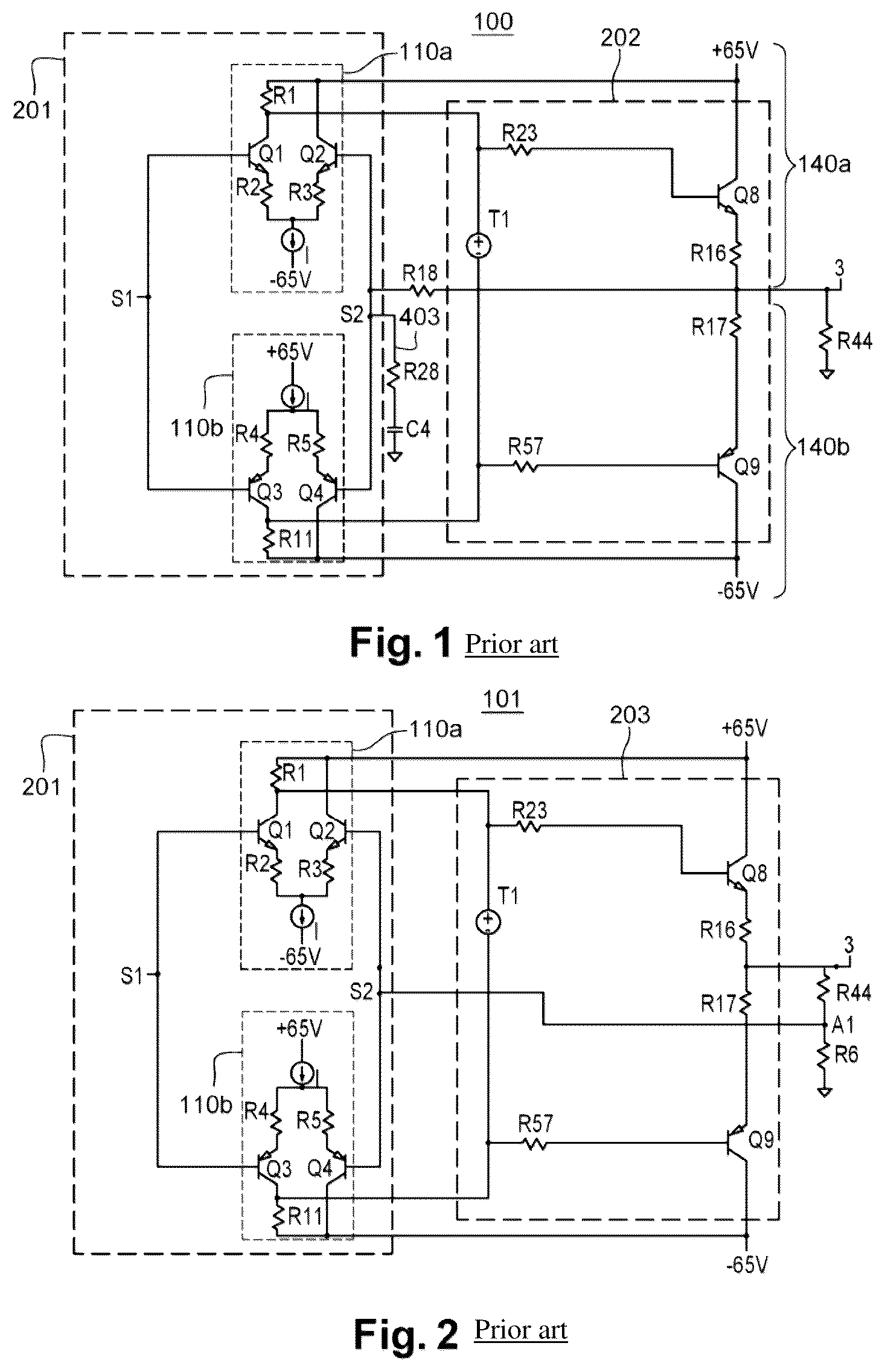
Thus, by way of example, illustrates a high-power amplifier 100 whose input signal is applied at point S 1 . The output of the high-power amplifier 100 powers a loudspeaker, represented by a resistor R 44 , connected between a point 3 and ground.
The diagram of the high-power amplifier 100 is symmetrical; it comprises as well an upper part 140 a , which amplifies the positive half-wave of the input signal S 1 , and a lower part 140 b , which amplifies the negative half-wave of the input signal S 1 .
In the example of , the high-power amplifier 100 is powered by a single voltage level of +/−65 V.
The pre-amplification stage 201 comprises two differential pairs 110 a , 110 b each comprising two transistors Q 1 , Q 2 and Q 3 , Q 4 assembled mirroring each other. Thus, the emitter of the transistors Q 1 , Q 2 is connected to the −65V power bus via a resistor R 2 , R 3 and a first constant current source I, while the emitter of the transistors Q 3 , Q 4 is connected to the +65V power bus via a resistor R 4 , R 5 and a second current source of same value I.
The collector of the transistors Q 2 , Q 4 is respectively connected to the +65V and −65V power bus, while the collector of transistors Q 1 , Q 3 is respectively connected to the +65V and −65V power bus via a resistor R 1 , R 11 . In the absence of feedback, the gain of the pre-amplification stage 201 depends on the ratio of the resistors R 1 /R 2 and R 11 /R 4 .
The bases of the transistors Q 1 and Q 3 and the bases of the transistors Q 2 and Q 4 are connected to each other. The bases of the transistors Q 1 and Q 3 are also powered by the input signal S 1 . The bases of the transistors Q 2 and Q 4 are connected to the loudspeaker R 44 via a resistor R 18 , so as to form the feedback applied to the pre-amplification stage. The collectors of the transistors Q 1 and Q 3 ensure the coupling of the pre-amplification stage 201 with the power amplification stage 202 .
The power amplification stage 202 comprises two transistors Q 8 , Q 9 connected by their respective bases to the pre-amplification stage 201 via a resistor R 23 , R 57 . A voltage source T 1 is also placed between the resistors R 23 and R 57 so as to bias the transistors Q 8 , Q 9 in class AB. This voltage source T 1 makes it possible to supply a voltage equal to the sum of the voltages necessary to turn on the transistors Q 8 and Q 9 .
The transistors Q 8 , Q 9 are also connected respectively to the +65 V and −65V power buses by their collector. The emitter of the transistors Q 8 , Q 9 is connected to the loudspeaker R 44 via resistors R 16 , R 17 . These resistors R 16 and R 17 are added in order to control the quiescent current, that is to say the value of the current conducted by the amplifier when it does not receive any input signal. Without these resistors R 16 , R 17 , the quiescent current would depend on the characteristics of the transistors Q 8 and Q 9 and the temperature, which is prohibitive.
In addition, the circuit in has a particularity at the bases of the transistors Q 2 and Q 4 . In fact, the latter are connected to a protection line 403 comprising a resistor R 28 assembled in series with a capacitor C 4 connected to ground. This assembly is a voltage divider such that the voltage at point S 2 is equal to R 28 /(R 18 +R 28 ) multiplied by the voltage of the output signal 3 in AC. In practice, the capacitor C 4 behaves like a short circuit when the voltage running through the circuit is alternating. On the other hand, when the voltage running through the circuit is DC, the capacitor C 4 behaves like an open circuit. In this case, the output signal 3 of the high-power amplifier 100 is directly connected to point S 2 . The voltage gain of the high-power amplifier 100 is then equal to 1, which makes it possible to limit a possible undesirable DC component on the voltage applied at the terminals of the loudspeaker R 44 .
In this type of amplifier, the voltage measured relative to ground at point S 1 and the voltage measured relative to ground at point S 2 are equal. In other words, the gain of the high-power amplifier 100 is equal to the ratio of the values of the resistors (R 18 +R 28 )/R 28 .
therefore illustrates a high-power voltage amplifier. There is also another category, high-power current amplifiers, as shown in .
This category of high-power current amplifiers 101 has the same topology as for the high-power voltage amplifiers 100 , namely a pre-amplification stage 201 coupled to an amplification stage 203 .
Unlike the high-voltage amplifier 100 of , a current measurement resistor R 6 is inserted between the loudspeaker R 44 and ground. Furthermore, the current amplifier 101 does not have a protection line 403 . The bases of the transistors Q 2 and Q 4 are connected to an interconnection point P 1 located between the resistor R 6 and the loudspeaker R 44 .
In this configuration, an image of the current applied at point S 2 in therefore crosses the loudspeaker R 44 . It follows that the transconductance, that is to say the ratio between the output current passing through the loudspeaker R 44 and the input voltage applied at point S 1 of the amplifier 101 is equal to 1/R 6 A/V. For a loudspeaker with impedance Z, the voltage gain is Z/R 6 .
The voltage or current amplification assemblies are therefore similar, particularly with regard to the pre-amplification stage and the power amplification stage. They only differ with regard to the loudspeaker connection and the feedback.
In the following prior art, the other classes of amplifiers will be described with reference to voltage amplifiers, although the invention is not limited to this type of amplifier.
A class system can be used to characterize different high-power amplifier topologies. The class system assigns a letter based on the relationship between the shape of the input signal and the shape of the output signal, as well as the duration for which active components are used during the amplification of the input signal.
Among the existing amplifier classes, class A amplifiers have a topology such that the active components conduct, in the absence of an input signal, a high current of approximately 50% of the maximum output current. This is called quiescent current. In modulation, the latter is superimposed on the output current. This type of amplifier can provide excellent sound quality, but it has the disadvantage of generating significant heat dissipation. Thus, the energy efficiency, defined by the ratio between the effective output power and the absorbed power, of this class of amplifiers is approximately 10%.
Class B amplifiers feature a topology such that the active components conduct over 50% of the input signal period when a sinusoidal input signal is applied as input. For this class of amplifiers, the quiescent current is zero. The efficiency of this type of amplifier is higher than class A amplifiers, but the distortion characteristics of the output signal are significantly degraded compared to class A amplifiers. Class B amplifiers therefore produce poorer quality sound. It is now quite rare for manufacturers to use this class of amplifier.
Class AB amplifiers feature a topology such that the active components conduct over 100% of the input signal period but with a low quiescent current of approximately 1% of the maximum output current. This type of amplifier has higher energy efficiency than class A amplifiers, typically between 30 and 50%, but lower sound quality. Class AB amplifiers are therefore a good compromise between performance and energy efficiency.
For class D amplifiers, a technology where the active components are operated like switches is used. The signal is then converted by pulse width modulation. This system increases energy efficiency to around 70%. On the other hand, the output signal contains more noise and distortion and it is difficult to reproduce high frequencies with this class of amplifiers.
Class G amplifiers have several power buses and can switch from one to another depending on the power output demand. This makes it possible to increase the energy efficiency by reducing the power dissipated in the active components.
Class H amplifiers use a power bus whose supply voltage “follows” or is modulated by the input signal. Typically, they have two power buses, like those of class G, but only the highest supply voltage is modulated. The modulated power supply is generally achieved using a class D amplifier.
The subject matter of the invention relates in particular to these last two categories of amplifiers.
illustrates the upper part of a power amplification stage 204 . The latter is connected to a power supply circuit 150 . Of course, this power amplification stage also comprises a lower part, not shown, mirroring the upper part with an equivalent power supply circuit. Likewise, the circuit also comprises a pre-amplification stage, for example connected to an independent power supply or to a strong power bus, also connected to the power supply circuit 150 .
The power supply circuit 150 makes it possible to select a power level of the power amplification stage 204 adapted to the amplification power demand. Thus, when the amplification voltage is greater than a threshold value, the first strong power bus must be used whereas, when the amplification voltage is lower than this threshold value, a second weaker power bus can be used. The lower power bus usage phases improve the overall efficiency of the amplifier compared to class A, B, and AB amplifiers.
Furthermore, the power supply circuit 150 has a structure independent of the pre-amplification stage 201 and the power amplification stage 204 . In the example of , the power amplification stage 204 comprises a transistor Q 10 whose base is connected to the emitter of the transistor Q 8 . This so-called “Darlington” configuration makes it possible to increase the current gain. The emitters of the transistors Q 8 and Q 10 are coupled to the loudspeaker R 44 by their respective resistors R 16 and R 19 . They have, for example, a respective quiescent currents equal to 6 mA for the transistor Q 8 and equal to 75 mA for the transistor Q 10 .
The power amplification stage 204 is connected to the power supply circuit 150 at the collectors of the transistors Q 8 and Q 10 . This power supply circuit 150 is connected to two voltage buses having distinct levels V+, V++. The power supply circuit 150 therefore makes it possible to select one or the other of these voltage levels depending on the amplification demand. Typically, a first power bus delivers 65 V and a second power bus delivers 35 V. The second power bus is intended to be used to power the power amplification stage 204 when the output signal to be generated does not have a very high voltage, typically less than 32 V.
Due to the relatively low current passing through the transistor Q 8 , typically less than 10% of the current passing through the transistor Q 10 , the collector of the transistor Q 8 can be directly connected to the first power bus V++, without this causing significant additional power dissipation. This embodiment can improve the stability of the amplifier, which operation as a current amplifier tends to undermine.
In order to select the appropriate voltage level, a MOSFET transistor M 1 is directly connected to the first power bus V++ by its drain and to the second power bus V+ by its source via a fourth diode D 3 . The MOSFET transistor M 1 typically switches for a threshold of 27 V, then it operates linearly beyond this threshold. It lets the first power bus V++ pass when a control voltage greater than a threshold value is applied at it. This voltage is controlled by the association of the first diode D 8 , D 10 , which is connected between the gate of the MOSFET transistor M 1 and the loudspeaker R 44 , and a second resistor R 8 , R 27 , which is connected between the drain and the gate of the MOSFET transistor M 1 .
A diode D 15 is connected between the collector of the transistor Q 10 and the loudspeaker R 44 , the cathode of the diode being connected to the collector of the transistor Q 10 .
The different signals obtained with this assembly are illustrated in .
Thus, the signal numbered 1 in represents the gate signal of the MOSFET transistor M 1 . The output signal numbered 3 in represents the output signal of the amplifier, that is to say the signal at the terminals of the loudspeaker R 44 . The output signal numbered 2 in represents the output signal of the power supply circuit 150 . We thus notice that the output signal 3 is distorted. Indeed, the crest of the sinusoid is flattened and shifts occur around 27 μs. This saturation of output signal 3 is explained by the fact that the supply voltage of the MOSFET transistor M 1 is insufficient for the amplifier to be able to deliver the output voltage correctly.
Likewise, the signal 2 has, between 40 and 47 μs, an abnormal voltage peak corresponding to an overvoltage at the gate of MOSFET transistor M 1 . This leads to a loss of power and a degradation in the efficiency of the amplifier.
The technical problem that the invention proposes to solve is therefore to obtain a high-power audio amplifier making it possible to limit the distortions identified on the signals and therefore to improve the efficiency and reduce the saturation of the amplifier.
DISCLOSURE OF THE INVENTION
To solve this problem, the invention proposes a power supply circuit comprising a MOSFET transistor controlled by a sub-circuit for assisting with charging, a sub-circuit for assisting with discharging and a voltage-shifting sub-circuit, making it possible to obtain better efficiency of the amplifier while limiting saturation and distortion of the amplifier output signal.
In other words, the invention relates to a high-power audio amplifier intended to control at least one loudspeaker, said amplifier comprising:
•
• a pre-amplification stage receiving an input signal; • a power amplification stage connected to the pre-amplification stage and providing an output signal intended to power said at least one loudspeaker; the pre-amplification and power amplification stages having a mirror-mounted upper part and lower part; • feedback providing the pre-amplification stage with an image of the output signal, • an upper power supply circuit, connected to the upper part of the power amplification stage, and allowing it to be powered by a first or a second power bus; • a lower power supply circuit connected to the lower part of the power amplification stage and allowing it to be powered by a first or a second power bus; • each power supply circuit comprising a MOSFET transistor and monitoring means, the MOSFET transistor being controlled by the monitoring means so as to carry out switching between one or the other of the two power buses, the MOSFET transistor being connected to the second power bus via a fourth diode, a first terminal of which is connected to the source of the MOSFET transistor, and the drain of the MOSFET transistor being connected to the first power bus.
The invention is characterized in that each power supply circuit further comprises:
•
• a sub-circuit for assisting with charging said MOSFET transistor comprising at least a first resistor, a first terminal of the first resistor being connected to the gate of the MOSFET transistor and a second terminal of the first resistor being connected to an interconnection point; • a sub-circuit for assisting with discharging said MOSFET transistor comprising at least a second and a third resistor and a bipolar transistor; the base of the bipolar transistor being connected to a first terminal of the third resistor, its emitter being connected to the gate of the MOSFET transistor and its collector being connected to the source of the MOSFET transistor via the second resistor, the second terminal of the third resistor being connected to the interconnection point; and • a voltage-shifting sub-circuit comprising a first diode mounted in parallel with a first capacitor; a first terminal of the first diode and a first terminal of the first capacitor being connected to a first interconnection node; a second terminal of the first diode and a second terminal of the first capacitor being connected to a second interconnection node.
In particular, the sub-circuit for assisting with charging allows the MOSFET transistor to charge faster. Indeed, it comprises first of all the first resistor, which preferably has a resistance of high value so as not to exchange too much energy with the output of the amplifier and generate more distortion, i.e. approximately 15 kΩ. This first resistor only allows a low current to run to charge or discharge the gate of the MOSFET transistor. The gate behaves like a capacitor, however, the combination of the MOSFET transistor with the first resistor increases the duration of the charging and discharging times.
The sub-circuit for assisting with discharging allows the MOSFET transistor to discharge faster. The bipolar transistor makes it possible in particular to discharge the gate of the MOSFET transistor when the sinusoidal input signal is in its decreasing phase.
The voltage-shifting sub-circuit ensures that the gate potential of the MOSFET transistor is always higher than that of the amplifier output. Typically, the gate potential of the MOSFET transistor can be 15 V higher than that of the amplifier output. The voltage-shifting sub-circuit also compensates for voltage drops in the MOSFET transistor.
According to a second embodiment, the voltage-shifting sub-circuit further comprises at least a fourth resistor and a second diode, mounted in parallel. A first terminal of the second diode and a terminal of the fourth resistor are connected to the first interconnection node, a second terminal of the fourth resistor and a second terminal of the second diode being connected to a third interconnection node.
The addition of these components makes it possible to reduce the distortions observed on the amplifier output signal. This improvement in distortion is effective for a sinusoidal input signal, if it is of relatively low frequency, that is to say around 1 kHz.
Advantageously, according to a third embodiment, the sub-circuit for assisting with charging further comprises a fifth resistor mounted in series with a third diode, the fifth resistor and the third diode being mounted in parallel with the branch of the sub-circuit for assisting with charging including the first resistor.
The third diode, which is mounted in parallel with the first resistor, allows the current intended to charge the gate of the MOSFET transistor to run and to block the current intended to discharge the gate of the MOSFET transistor. The fifth resistor is preferably of low value, that is to say approximately 300Ω. This fifth resistor makes it possible to charge the gate of the MOSFET transistor much faster, since the charging time constant is equal to the product of the resistance and the capacitance.
The addition of these components here again makes it possible to improve the distortion for a sinusoidal input signal up to a frequency of 20 kHz. Distortion is therefore improved across the entire frequency spectrum. The sound reproduction of a loudspeaker connected to the amplifier of the invention is therefore improved. The listener perceives less distortion compared to amplifiers of the prior art.
According to a fourth embodiment, the voltage-shifting sub-circuit further comprises a second capacitor and a third capacitor, the second capacitor being mounted in parallel with the first capacitor and the first diode and the third capacitor being mounted in parallel with the third diode and the fifth resistor. These additional components make it possible to limit disturbances, that is to say interference signals superimposed on the expected output signal.
In practice, each power supply circuit comprises a first protection diode, a first terminal of which is connected to the source of the MOSFET transistor and a second terminal of which is connected to the gate of the MOSFET transistor. Likewise, each power supply circuit further comprises a second protection diode connected between the source and the drain of the MOSFET transistor.
The first protection diode is added in order to protect the MOSFET transistor from overvoltages on its gate, which could damage it or even make it unusable, by breaking the insulation between the gate and the channel which can only withstand +/−20 V continuously and +/−30 V transiently.
The role of the second protection diode is to protect the MOSFET transistor from a reverse drain-source voltage which could occur if the voltage of the first power bus only appears after that of the second power bus. The different power buses each have their own transformer windings and smoothing capacitors, hence different time constants.
According to a fifth embodiment, each power supply circuit further comprises a capacitor mounted in parallel with the fourth diode. This capacitor makes it possible to eliminate the interference peaks generated by the diode, a first terminal of which is connected to the source of the MOSFET transistor, when the latter switches. The harmonic distortion (THD) is also improved. This harmonic distortion is a measure of the linearity of the processing carried out. It is calculated by comparing the output signal of a device with a perfectly sinusoidal input signal.
In practice, the pre-amplification stage is connected to the first power bus of each power supply circuit via a circuit for damping power variations of said first power bus, said power variation damping circuit comprising at least one capacitor and at least one resistor mounted as a low-pass filter. In other words, the resistor is connected in series with the capacitor, which is connected to ground.
This assembly makes it possible to isolate noise and voltage dips. This phenomenon occurs in particular when the high-voltage amplifier delivers a high current. The capacitor then plays the role of an energy reservoir.
Advantageously, said power variation damping circuit further comprises an additional capacitor mounted in parallel with the at least one capacitor. The capacitor mounted in parallel has a more modest value, typically lower by a factor of 10 3 . It enables one to suppress high-frequency interference.
According to a specific embodiment of the invention, the feedback applied to the pre-amplification stage supplies a signal proportional to the current passing through the loudspeaker. This embodiment makes it possible to obtain a high-power current amplifier. As described with reference to of the prior art, this category of high-power current amplifiers has the same topology as for high-power voltage amplifiers, namely a pre-amplification stage coupled to an amplification stage. However, the feedback applied to the pre-amplification stage differs.
By using the power supply circuit of the invention for a high-power current amplifier, the high-power current amplifier has very limited consumption.
Indeed, when the amplifier delivers a low voltage, the power supply circuit of the invention will not be active. Thus, the power supplied by the power supply will be equal to the product of the output current multiplied by the voltage delivered by the power bus of lower power, instead of the maximum voltage delivered by the single power bus for a standard class AB amplifier. At equal power, and assuming for example that the voltage delivered by the lower power power bus is equal to half that of the higher power power bus, half as much power will be supplied by the power supply. The transistors, which dissipate the difference between the power supplied by the power supply and the power supplied to the loudspeaker, will heat up significantly less.
BRIEF DESCRIPTION OF THE FIGURES
The manner of embodying the invention, as well as the advantages which result therefrom, will appear clearly from the description of the following embodiments, in support of the appended figures in which:
is an electrical diagram of a high-power voltage amplifier of the prior art,
is an electrical diagram of a high-power current amplifier of the prior art,
is an electrical diagram of a high-power voltage amplifier of the prior art comprising a power supply stage,
is a graph representing the evolution of the gate voltage of the MOSFET transistor, the output voltage of the amplifier, and the output signal of the power supply circuit for the circuit of .
a and [ b ] are electrical diagrams of the high-power voltage amplifier according to one embodiment of the invention,
is an electrical diagram of the power supply circuit of the high-power amplifier according to a second embodiment,
is a graph representing the evolution of the gate voltage of the MOSFET transistor, the output voltage of the amplifier, and the output signal of the power supply circuit for the circuit of with a sinusoid of frequency 20 kHz at the input,
is a graph representing the evolution of the gate voltage of the MOSFET transistor, the output voltage of the amplifier, and the output signal of the power supply circuit for the circuit of with a sinusoid of frequency 1 kHz at the input,
is an electrical diagram of the power supply circuit of the high-power amplifier according to a third embodiment,
is a graph representing the evolution of the gate voltage of the MOSFET transistor, the output voltage of the amplifier, and the output signal of the power supply circuit for the circuit of with a sinusoid of frequency 20 kHz at the input,
is a graph representing the evolution of the gate voltage of the MOSFET transistor, the output voltage of the amplifier, and the output signal of the power supply circuit for the circuit of with a sinusoid of frequency 1 kHz at the input,
is an electrical diagram of the power supply circuit of the high-power amplifier according to a fourth embodiment,
is a graph representing the evolution of the gate voltage of the MOSFET transistor, the output voltage of the amplifier, and the output signal of the power supply circuit for the circuit of with a sinusoid of frequency 20 kHz at the input,
is an electrical diagram of the power supply circuit of the high-power amplifier according to a fifth embodiment,
is a graph representing the evolution of the gate voltage of the MOSFET transistor, the output voltage of the amplifier, and the output signal of the power supply circuit for the circuit of with a sinusoid of frequency 20 kHz at the input,
is an electrical diagram of the power supply circuit of the high-power amplifier according to the first embodiment of ,
is a graph representing the evolution of the gate voltage of the MOSFET transistor, the output voltage of the amplifier, and the output signal of the power supply circuit for the circuit of with a sinusoid of frequency 20 kHz at the input,
a and [ b ] are electrical diagrams of the high-power current amplifier according to an embodiment of the invention, and
is an electrical diagram of a protection structure of a high-power current amplifier according to an embodiment of the invention.
DETAILED DESCRIPTION OF THE EMBODIMENTS
As illustrated in a - 5 b , the high-power amplifier 102 of the invention is symmetrical, it comprises an upper part, which amplifies the positive half-wave of the input signal S 1 , and a lower part, which amplifies the negative half-wave of the input signal S 1 .
The high-power amplifier 102 comprises a pre-amplification stage that receives the input signal S 1 and supplies signals coming from the collector of transistors Q 5 , Q 6 , via a network consisting of the resistor R 23 , R 57 , mounted in parallel with a capacitor C 7 , C 8 . These signals are supplied to a power amplification stage 302 based on transistor Q 8 , Q 9 . The latter supplies an output signal 3 intended to power a loudspeaker R 44 . A feedback supplies the pre-amplification stage 201 with an image of the output signal 3 .
The high-power amplifier 102 also comprises an upper power supply circuit 155 a , which is connected to the upper part of the power amplification stage 302 , and a lower power supply circuit 155 b , which is connected to the lower part of the power amplification stage 302 .
The pre-amplification stage 301 comprises two differential pairs 110 a , 110 b each comprising two transistors Q 1 , Q 2 and Q 3 , Q 4 mounted mirroring each other. Thus, the emitter of the transistors Q 1 , Q 2 is connected to the −65V power bus via a resistor R 2 , R 3 and a first constant current source I 1 , while the emitter of the transistors Q 3 , Q 4 is connected to the +65V power bus via a resistor R 4 , R 5 and a second current source of the same value I 1 .
The current sources I 1 and 12 each comprise a transistor Q 23 , Q 24 whose collector is respectively connected to the resistors R 2 , R 3 and R 4 , R 5 . The emitter of the transistors Q 23 , Q 24 is connected to a resistor R 6 , R 10 . The second terminal of the resistor R 6 is connected on the one hand to the −65V power bus and on the other hand to ground, via a capacitor C 11 mounted in series with a resistor R 46 . The second terminal of the resistor R 10 is connected on the one hand to the +65V power bus and on the other hand to ground, via a capacitor C 12 mounted in series with a resistor R 48 .
A diode D 1 , D 2 is mounted between the base of the transistor Q 23 , Q 24 and the second terminal of the resistor R 6 , R 10 , while a resistor R 45 , R 47 is mounted between the base of the transistor Q 23 , Q 24 and the interconnection point between the capacitor C 11 , C 12 and the resistor R 46 , R 48 .
The collector of the transistors Q 2 , Q 4 can be directly connected, respectively, to the +65V and −65V power bus. Alternatively, the collector of the transistors Q 2 , Q 4 can be connected, respectively, to the +65V and −65V power bus via a power variation damping circuit 304 , 305 .
The power variation damping circuit 304 , 305 comprises a resistor R 52 , R 55 mounted in series with a capacitor C 15 , C 19 which is connected to ground. The second terminal of the resistor R 52 , R 55 is connected to the +/−65V power bus. Advantageously, another capacitor C 16 , C 20 can be mounted in parallel with the capacitor C 15 , C 19 . In practice, the capacitor C 15 , C 19 has a value between 150 and 300 μF, while the capacitor C 16 , C 20 has a value between 150 and 300 nF.
The collector of the transistors Q 1 , Q 3 is respectively connected to the +65V and −65V power bus via a resistor R 1 , R 11 and advantageously via the power variation damping circuit 304 , 305 . In the absence of feedback, the gain of the first pre-amplification stage 102 depends on the ratio of the resistors R 1 /R 2 and R 11 /R 4 .
The bases of the transistors Q 1 and Q 3 are connected to each other and connected to ground via a resistor R 7 . The bases of the transistors Q 2 and Q 4 are also connected to each other. The bases of the transistors Q 1 and Q 3 are supplied with the input signal S 1 . The voltage source V 1 , connected between the point S 1 and ground, represents the generator of the input signal S 1 . An intermediate filter circuit can be inserted between the input signal S 1 and the bases of the transistors Q 1 and Q 3 . This circuit comprises for example a band-pass filter comprising a resistor R 9 and a capacitor C 10 which is connected to ground, and two capacitors C 1 , C 6 , mounted in parallel.
The bases of the transistors Q 2 and Q 4 are connected to the loudspeaker R 44 via a resistor R 18 , so as to form the feedback applied to the pre-amplification stage 301 . The collectors of the transistors Q 1 and Q 3 ensure the coupling of the pre-amplification stage 301 with the circuits 306 , 303 , 307 and the resistors R 12 , R 13 .
The power amplification stage 302 comprises two transistors Q 8 , Q 9 connected by their respective bases to the pre-amplification stage 301 via the circuit 306 , 307 .
The circuit 306 , 307 comprises a transistor Q 5 , Q 6 whose emitter is connected to the +/−65V voltage bus via a resistor R 12 , R 13 and whose base is connected to the collector of the transistors Q 1 , Q 3 . A capacitor C 2 , C 3 is connected between the base and the collector of the transistors Q 5 , Q 6 in order to improve the stability of the amplifier. The collector of the transistors Q 5 , Q 6 is connected, on the one hand, to a resistor R 57 , R 23 mounted in parallel with a capacitor C 8 , C 7 and, on the other hand, to a bias circuit 303 . The latter comprises a transistor Q 7 whose emitter is connected to the collector of the transistor Q 5 and whose collector is connected to the collector of the transistor Q 6 . A resistor R 14 is mounted between the collector and the base of the transistor Q 7 and another resistor R 15 is mounted between the emitter and the base of transistor Q 7 . Finally, a capacitor C 5 , for example having a value of 1 μF, is connected between the emitter and the collector of the transistor Q 7 . This capacitor C 5 improves the stability of the amplifier. Alternatively, the resistor R 13 , R 12 can be connected, respectively, to the +65V and −65V power bus via a power variation damping circuit 304 , 305 .
The circuits 306 , 307 carry out a second voltage amplification. The gain of this amplification is proportional to the ratio of the resistance “seen by the collector” to that present on the emitter of Q 5 , Q 6 . When one of the transistors Q 5 , Q 6 conducts, its dual is blocked; the transistor which is conducting therefore sees a very high resistance hence a very significant voltage gain.
The power amplification stage 302 further comprises two transistors Q 10 , Q 11 whose bases are respectively connected to the emitter of the transistors Q 8 and Q 9 . This so-called “Darlington” configuration makes it possible to increase the current gain. The emitters of the transistors Q 8 and Q 10 are coupled to the loudspeaker R 44 by their respective resistors R 16 and R 19 , while the emitters of the transistors Q 9 and Q 11 are coupled to the loudspeaker R 44 by their respective resistors R 17 and R 20 . For example, they have a respective quiescent current equal to 6 mA for the transistors Q 8 , Q 9 and equal to 75 mA for the transistors Q 10 , Q 11 .
The power amplification stage 302 is connected to two power supply circuits 155 a , 155 b at the site of the collectors of the transistors Q 8 -Q 11 . These power supply circuits 155 a , 155 b are connected to two voltage buses having distinct levels V+, V++. The power supply circuit 155 a , 155 b therefore makes it possible to select one or the other of these voltage levels depending on the amplification demand. Typically, a first power bus delivers +/−65V and a second power bus delivers +/−35V. The second power bus is intended to be used to power the power amplification stage 302 when the output signal to be generated does not have a very high voltage, typically less than 27 V.
Due to the relatively low current passing through the transistors Q 8 and Q 9 , typically less than 10% of the current passing through the transistors Q 10 and Q 11 , the collectors of Q 8 and Q 9 can be directly connected to the first power bus V++ without this causing significant additional power dissipation. This embodiment improves the stability of the amplifier in terms of its phase margin and its gain margin.
In addition, the bases of the transistors Q 2 and Q 4 are connected to a protection line comprising a resistor R 28 mounted in series with a capacitor C 4 connected to ground. This assembly is a voltage divider. In practice, the capacitor C 4 behaves like a short circuit when the voltage running through the circuit is alternating. On the other hand, when the voltage running through the circuit is DC, the capacitor C 4 behaves like an open circuit. In this case, the output of the high-power amplifier 100 is directly connected to the point S 2 . The voltage gain of the high-power amplifier 100 is then equal to 1, which makes it possible to limit a possible undesirable DC component on the voltage applied to the terminals of the loudspeaker R 44 .
Several embodiments are possible for the power supply circuit 151 - 155 , 155 a , 155 b.
For all the following embodiments, the signal numbered 1 represents the gate signal of the MOSFET transistor M 1 , M 2 . The output signal numbered 3 represents the output signal of the amplifier, that is to say the signal at the terminals of the loudspeaker R 44 . The output signal numbered 2 represents the output signal of the power supply circuit 151 - 155 , 155 a , 155 b , that is to say the signal present on the collector of the transistors Q 8 and Q 10 .
In the remainder of the description, only the upper power supply circuit is illustrated but a - 5 b makes it possible to understand the positioning of the corresponding components for the lower power supply circuit.
As illustrated in , in a first embodiment, the power supply circuit 151 comprises a MOSFET transistor M 1 , M 2 which is directly connected to the first power bus V++ by its drain and to the second power bus V+ by its source via a fourth diode D 3 , D 11 , which can be a conventional diode or a Schottky diode. In practice, the anode of the fourth diode D 3 is connected to the second power bus V+ and its cathode is connected to the output signal numbered 2 representing the output signal of the power supply circuit 151 - 155 , 155 a , 155 b ; the cathode of the fourth diode D 11 is connected to the second power bus-V+. The MOSFET transistor M 1 , M 2 is blocked for a voltage below a threshold, typically 35 V, then switches and operates linearly beyond this threshold. The MOSFET transistor M 1 , M 2 allows the first power bus V++ to pass when a control voltage greater than the threshold value is applied to it. This voltage is controlled by the association of a sub-circuit for assisting with charging 131 , a sub-circuit for assisting with discharging 141 and a voltage-shifting sub-circuit 161 .
The sub-circuit for assisting with charging 131 comprises a first resistor R 24 , R 31 connected between the gate of the MOSFET transistor M 1 , M 2 and an interconnection point A 1 , A 2 .
The sub-circuit for assisting with discharging 141 comprises a transistor Q 12 , Q 13 whose emitter is connected on the one hand to the gate of the MOSFET transistor M 1 , M 2 and on the other hand to the sub-circuit for assisting with charging 131 . The collector of the transistor Q 12 , Q 13 is connected to output signal 2 of the power supply circuit 151 via the second resistor R 8 , R 27 . The base of the transistor Q 12 , Q 13 is connected to the interconnection point A 1 , A 2 via a third resistor R 21 , R 39 .
The voltage-shifting sub-circuit 161 comprises a first capacitor C 18 , C 23 mounted in parallel with a first diode D 8 , D 10 . The cathode of the first diode D 8 is connected to a first interconnection node N 1 and the anode of the first diode D 8 is connected to a second interconnection node N 2 . The diode D 10 is connected in reverse, that is to say its cathode is connected to the interconnection node N 3 and its anode is connected to the interconnection node N 4 , as shown in a - 5 b . The first interconnection node is connected to the interconnection point A 1 and the second interconnection node is connected to the loudspeaker R 44 .
The voltage-shifting sub-circuit ensures that the gate potential of the MOSFET transistor M 1 is always 15 V higher than that of the amplifier output.
In addition, the Darlington circuit consisting of the transistors Q 8 and Q 10 requires 5 V of drop-out voltage, that is to say the voltage equal to the difference between the input voltage on the collector of the transistor Q 8 and the output voltage of the emitter of the transistor Q 10 . The MOSFET M 1 , on the other hand, requires 10 V of drop-out voltage, that is to say the voltage equal to the difference between the input voltage on its gate and the output voltage on its source in the case where the current is maximum and saturated. The voltage-shifting sub-circuit must therefore compensate for the voltage drops of the two bipolar transistors Q 8 and Q 10 , as well as of the MOSFET M 1 , i.e. 5+10=15 V.
The power supply circuit 151 advantageously comprises a first protection diode D 5 , D 13 . The anode of diode D 5 is connected to the output signal 2 of the power supply circuit 151 and its cathode is connected to the gate of the MOSFET transistor M 1 . The cathode of diode D 13 is connected to the output of the power supply circuit 155 b and its anode is connected to the gate of the MOSFET transistor M 2 . Likewise, the power supply circuit 151 includes a second protection diode D 4 , D 12 . The cathode of the diode D 4 is connected to the source of the MOSFET transistor M 1 and its anode is connected to the source of the MOSFET transistor M 1 . The cathode of the diode D 12 is connected to the source of the MOSFET transistor M 2 and its anode is connected to the drain of MOSFET transistor M 2 .
With such an assembly, the different signals obtained are illustrated in .
The signals illustrated in correspond to the signals obtained with a sinusoid of frequency 20 kHz supplied at the input of the high-power amplifier 102 .
We thus notice that the output signal 3 is distorted at the site of the vertices of the sinusoids which take on a triangular appearance. Thus, it is not possible to correctly reproduce a 20 kHz sinusoid. On the other hand, we do not observe abnormal voltage peaks. Power losses are therefore limited.
The signals illustrated in correspond to the signals obtained with a sinusoid of frequency 1 kHz supplied at the input of the high-power amplifier 102 .
We thus notice that the output signal 3 is less distorted than at 20 kHz. To the naked eye, the sinusoid of the output signal 3 even seems perfectly reproduced. However, it turns out that the harmonic distortion (THD) is greater than 0.1%.
As illustrated in , in a second embodiment, the voltage-shifting sub-circuit 162 of the power supply stage 152 further comprises a second diode D 6 , D 29 mounted in parallel with a fourth resistor R 22 , R 26 . The cathode of the second diode D 6 is connected to the interconnection point N 1 and the anode of the second diode D 6 is connected to the third interconnection node N 10 . The diode D 29 is connected in reverse, that is to say its cathode is connected to the interconnection node N 20 and its anode is connected to the interconnection node N 4 , as illustrated in a - 5 b.
With such an assembly, the different signals obtained are illustrated in . The signals illustrated in correspond to the signals obtained with a sinusoid of frequency 20 kHz supplied at the input of the high-power amplifier 102 .
We thus notice that the output signal 3 is distorted at the site of the vertices of the sinusoids which take on a triangular appearance. Thus, it is not possible to correctly reproduce a 20 kHz sinusoid.
The signals illustrated in correspond to the signals obtained with a sinusoid of frequency 1 kHz supplied at the input of the high-power amplifier 102 .
To the naked eye, the sinusoid of the output signal 3 appears to be perfectly reproduced on the positive half-wave and slightly distorted on the negative half-wave. The harmonic distortion THD is equal to 0.45% because the observed distortion corresponds to the production of harmonics.
The addition of these components therefore does not help to reduce the distortions observed on the amplifier output signal. The addition of the second diode D 6 , D 29 and the fourth resistor R 22 , R 26 degrades the dynamic performance of the circuit. More complex circuitry is required for these components to be beneficial, that is to say for them to improve low frequency and high frequency degradation. To obtain a performance gain, it is possible to add other elements around the transistor Q 12 , Q 13 .
As illustrated in , in a third embodiment, the sub-circuit for assisting with the charging 132 of the power supply stage 153 further comprises a circuit branch comprising a third diode D 9 , D 14 in series with a fifth resistor R 29 , R 30 , which is mounted in parallel with the first resistor R 24 , R 31 . The cathode of the third diode D 9 is for example connected to the gate of the MOSFET transistor M 1 . The anode of the third diode D 14 is connected to the gate of the MOSFET transistor M 2 . Alternatively, the components D 9 , R 29 and D 14 , R 30 can be reversed, so that the third diode D 9 , D 14 is connected to the gate of the MOSFET transistor M 1 , M 2 via the resistor R 29 , R 30 .
With such an assembly, the different signals obtained are illustrated in . The latter correspond to the signals obtained with a sinusoid of frequency 20 kHz provided at the input of the high-power amplifier 102 .
We observe that the output sinusoid corresponding to the output signal numbered 3 is well restored. On the other hand, the output signal 2 , representing the output voltage of the power supply circuit 153 , has distortions between 0 and 5 us and between 18 and 20 μs. The THD is equal to 0.26%. The addition of these components here makes it possible to improve the distortion for a sinusoidal input signal up to a frequency of 20 KHz.
As illustrated in , in a fourth embodiment, the voltage-shifting sub-circuit of the power supply stage 154 further comprises a third capacitor C 21 , C 24 , which is mounted in parallel with the fourth resistor R 22 , R 26 and the second diode D 6 , D 29 , as well as a second capacitor C 17 , C 22 , which is mounted in parallel with the first diode D 8 , D 10 and the first capacitor C 18 , C 23 .
The different signals obtained with such an assembly are illustrated in . The latter correspond to the signals obtained with a sinusoid of frequency 20 kHz supplied at the input of the high-power amplifier 102 .
We thus observe that the signal 2 is less disturbed but the switching of the fourth diode D 3 still generates interference, particularly between 45 and 50 μs.
Indeed, the second capacitor C 17 , C 22 , for example using the electrochemical technology, has a significant value, typically between 5 and 15 μF, and constitutes an energy reservoir, while the first capacitor C 18 , C 23 , for example using the electrochemical plastic film technology, has a lower value, typically between 50 and 150 nF, and makes it possible to smooth out high-frequency interference. The THD is reduced to 0.21%.
This association makes it possible to make the circuit more efficient in the transient phases of signal growth and decay.
As illustrated in a - 5 b and 16 , in a fifth embodiment, the power supply stage 155 , 155 a , 155 b further comprises a fourth capacitor C 14 , C 25 which is mounted in parallel with the fourth diode D 3 , D 11 .
The different signals obtained with such assembly are illustrated in . The latter correspond to the signals obtained with a sinusoid of frequency 20 kHz supplied at the input of the high-power amplifier 102 .
We observe that the interference generated by the fourth diode D 3 , D 11 has disappeared between 45 and 50 μs. This results in a slight drop in the THD from 0.21 to 0.2%.
Although the invention has been described in the preceding with reference to a - 5 b to 17 for a high-power audio amplifier 102 making it possible to supply a loudspeaker R 44 with voltage, it is also possible to use the power supply circuit of the invention for a high-power current audio amplifier, that is to say to supply current to a loudspeaker.
To do this, as illustrated in a - 18 b a current measurement resistor R 61 is inserted between the loudspeaker R 44 and ground. Furthermore, the current amplifier 103 does not have a protection line 403 . The bases of the transistors Q 2 and Q 4 are connected to an interconnection point located between the resistor R 61 and the loudspeaker R 44 via a capacitor C 40 . This capacitor C 40 therefore only allows the alternating component of the signal to pass.
In this configuration, the loudspeaker R 44 is therefore traversed by an alternating current, an image of which is applied to point S 2 . It follows that the transconductance of the amplifier is equal to 1/R 61 for an alternating signal.
Alternatively, in order to protect the loudspeaker R 44 and the amplifier itself, a resistor can be added to the feedback, between point S 2 and the output of the amplifier 3 . In the case of a DC component at the terminals of the loudspeaker R 44 , the DC component is applied at the bases of the transistors Q 2 and Q 4 via a resistor R 18 . The feedback will tend to cancel this DC component. In addition, the resistor R 18 helps limit the gain of the amplifier in the absence of loudspeaker R 44 , also preventing it from oscillating.
When the current is alternating, the capacitor C 40 has a negligible impedance compared to the value of the resistor R 18 . In normal operation, that is to say, when there is no DC component and when a loudspeaker R 44 is actually present at the amplifier output, the resistor R 18 has almost no effect. On the other hand, in the absence of loudspeaker R 44 at the amplifier output, we can consider that point S 2 is connected, on the one hand, to the amplifier output via the resistor R 18 , and, on the other hand, to ground via the resistor R 61 since the capacitor C 40 behaves like an alternating current short circuit. The voltage amplification will therefore be limited to (R 18 +R 61 )/R 61 since the output voltage of the amplifier multiplied by R 61 /(R 18 +R 61 ) is compared to the input voltage applied at point S 1 by the differential pairs formed by the transistors Q 1 /Q 2 and Q 3 /Q 4 . The amplifier will then not supply its maximum output voltage, which could have been dangerous. Likewise, in the presence of a DC component and in the presence or absence of loudspeaker R 44 at the output of the amplifier, the capacitor behaves like an open circuit, the DC component is thus reinjected at point S 2 via the resistor R 18 . The voltage gain is thus limited to 1 for DC voltages, which does not risk damaging the loudspeaker R 44 .
In another variant, a current amplifier protection circuit can be added. To do this, as illustrated in , the interconnection point P 1 located between the resistor R 61 and the loudspeaker R 44 is connected to a first terminal of a resistor R 70 . In this embodiment, the second terminal of the resistor R 70 is connected to the collector of a transistor Q 16 . The collector of the transistor Q 16 is also connected to the base of a second transistor Q 15 . The voltage divider is made up of the resistors R 71 and R 72 makes it possible to adapt the current threshold starting from which the protection circuit acts. The first terminal of the resistor R 71 is connected to the second power bus V+ with a value of 32 V. The second terminal of the resistor R 71 is connected to the base of the transistor Q 15 and to the collector of the transistor Q 16 . The first terminal of the resistor R 72 is connected to the second terminal of the resistor R 70 and the second terminal of the resistor R 72 is connected to ground. The conduction threshold voltage of the transistor Q 15 is thus shifted by: V+*R 72 /(R 71 +R 72 ). This makes it possible to increase the sensitivity, that is to say that the current threshold from which the protection acts is lowered.
Preferably, the transistor Q 15 is a Darlington transistor. This makes it possible to limit the distortion due to the circuit by drawing a lower current at the terminals of the measurement resistor R 61 while maintaining sufficient sensitivity thanks to the divider network R 71 /R 72 . Another divider bridge made up of the resistors R 73 and R 74 is inserted between point 3 and ground. The first terminal of resistor R 73 is connected to point 3 . The second terminal of the resistor R 73 is connected to the base of the transistor Q 16 and to the first terminal of the resistor R 74 . The second terminal of the latter is connected to ground. Thus, the voltage threshold starting from which the current protection is neutralized is adapted. The emitters of the transistors Q 16 and Q 15 are connected together and to ground, and the collector of the transistor Q 15 is connected to the base of the transistor Q 8 via a diode D 21 , the cathode of which is connected to the collector of the transistor Q 15 .
This circuit must be mirror-duplicated to manage the current protection during negative half-wave, the NPN transistors are then replaced by PNP transistors.
This circuit makes it possible to limit the risks of power failure of the current amplifier, particularly when it is overloaded or when its output is short-circuited. Indeed, in these cases, the product of the output current and the voltage of the power buses will be entirely dissipated by the transistors and they could be damaged.
With the circuit of , if the current in the current measurement resistor R 61 is sufficient to turn on the transistor Q 15 , the latter can, via the diode D 21 , evacuate the signal coming from the base of the transistor Q 8 towards ground, so as to block it. On the other hand, if the voltage at the terminals of the loudspeaker R 44 is sufficient to turn on the transistor Q 16 , the signal coming from the base of the transistor Q 15 will be diverted to ground and it is the latter transistor which will be blocked. The protection circuit is thus neutralized in the presence of sufficient voltage at the amplifier output.
To conclude, the invention makes it possible to obtain a high-power audio amplifier making it possible to limit the distortions identified on the signals and thus to improve the efficiency and reduce the saturation of the amplifier.
Figures (17)
Citations
This patent cites (3)
- US3974455
- US9236839
- US2024/0223206