Wireless Communication Device and Antenna Matching Circuit
Abstract
A wireless communication device and an antenna matching circuit are provided. The wireless communication device includes an RF transceiver, a first SPDT switch, a low noise amplifier, a power amplifier, and the antenna matching circuit. The antenna matching circuit includes a second SPDT switch, a first antenna element, a second antenna element, a first transmission path, a second transmission path, and a plurality of SPST switches. The second SPDT switch is connected to the first SPDT switch. When the antenna matching circuit is switched to a first mode, the second SPDT switch is switched to the first transmission path, and the first antenna element is used to generate a first radiation pattern. When the antenna matching circuit is switched to a second mode, the second SPDT switch is switched to the second transmission path, and the second antenna element is used to generate a second radiation pattern.
Claims (15)
1. A wireless communication device, comprising: a radio frequency transceiver; a first single pole double throw (SPDT) switch connected to the radio frequency transceiver; a low noise amplifier connected between the radio frequency transceiver and the first SPDT switch; a power amplifier connected between the radio frequency transceiver and the first SPDT switch; and an antenna matching circuit, wherein the antenna matching circuit is operable for an operating frequency and includes: a second SPDT switch connected to the first SPDT switch; a first antenna element and a second antenna element connected to the second SPDT switch; a first transmission path and a second transmission path, wherein the first transmission path is connected between the first antenna element and the second SPDT switch, and the second transmission path is connected between the second antenna element and the second SPDT switch; and a plurality of single pole single throw (SPST) switches connected between the first transmission path and the second transmission path; wherein, in response to the antenna matching circuit being switched to a first mode, the second SPDT switch is switched to the first transmission path, the SPST switches are in non-conducting states, and the first antenna element is used to generate a first radiation pattern; wherein, in response to the antenna matching circuit being switched to a second mode, the second SPDT switch is switched to the second transmission path, the SPST switches are in the non-conducting states, and the second antenna element is used to generate a second radiation pattern; wherein the first radiation pattern has a first polarization direction, the second radiation pattern has a second polarization direction, and the first polarization direction is orthogonal to the second polarization direction.
10. An antenna matching circuit, which is operable for an operating frequency, the antenna matching circuit comprising: a single pole double throw (SPDT) switch; a first antenna element and a second antenna element connected to the SPDT switch; a first transmission path and a second transmission path, wherein the first transmission path is connected between the first antenna element and the SPDT switch, and the second transmission path is connected between the second antenna element and the SPDT switch; and a plurality of single pole single throw (SPST) switches connected between the first transmission path and the second transmission path; wherein, in response to the antenna matching circuit being switched to a first mode, the SPDT switch is switched to the first transmission path, the SPST switches are in non-conducting states, and the first antenna element is used to generate a first radiation pattern; wherein, in response to the antenna matching circuit being switched to a second mode, the SPDT switch is switched to the second transmission path, the SPST switches are in the non-conducting states, and the second antenna element is used to generate a second radiation pattern; wherein the first radiation pattern has a first polarization direction, the second radiation pattern has a second polarization direction, and the first polarization direction is orthogonal to the second polarization direction.
Show 13 dependent claims
2. The wireless communication device according to claim 1 , wherein the first transmission path includes a first section, a second section, and a third section, the first section is connected to the second SPDT switch, the third section is connected to the first antenna element, the second section is connected between the first section and the third section, the second section intersects with the first section at a first connection point, the second section intersects with the third section at a second connection point, the second transmission path includes a fourth section, a fifth section, and a sixth section, the fourth section is connected to the second SPDT switch, the sixth section is connected to the second antenna element, the fifth section is connected between the fourth section and the sixth section, the fifth section intersects with the fourth section at a third connection point, the fifth section intersects with the sixth section at a fourth connection point, and lengths of the second section and the fifth section are both equal to one-fourth of a wavelength of the operating frequency.
3. The wireless communication device according to claim 2 , wherein the antenna matching circuit further includes a third transmission path, a fourth transmission path, and a fifth transmission path, the third transmission path is connected between the first connection point and the third connection point, the fourth transmission path is connected between the second connection point and the fourth connection point, lengths of the third transmission path and the fourth transmission path are both equal to one-fourth of the wavelength of the operating frequency, impedance values of the third transmission path and the fourth transmission path are greater than impedance values of the second section and the fifth section, and the fifth transmission path is connected to the second SPDT switch.
4. The wireless communication device according to claim 2 , wherein the antenna matching circuit further includes a third transmission path and a fourth transmission path, the third transmission path is connected between the first connection point and the third connection point, the fourth transmission path is connected between the second connection point and the fourth connection point, lengths of the third transmission path and the fourth transmission path are both equal to one-fourth of the wavelength of the operating frequency, the SPST switches include a first SPST switch, a second SPST switch, a third SPST switch, and a fourth SPST switch, the first SPST switch and the second SPST switch are connected in series in the third transmission path, and the third SPST switch and the fourth SPST switch are connected in series in the fourth transmission path.
5. The wireless communication device according to claim 4 , wherein the antenna matching circuit further includes a plurality of capacitors, and the second SPDT switch, the first SPST switch, the second SPST switch, the third SPST switch, and the fourth SPST switch include a plurality of terminals, and the capacitors are respectively connected to the terminals.
6. The wireless communication device according to claim 1 , wherein the antenna matching circuit further includes a circuit substrate, the circuit substrate has a first surface and a second surface that are opposite to each other, and the first transmission path, the second transmission path, the second SPDT switch, and the SPST switches are disposed on the first surface; wherein the first antenna element includes a first radiating portion, a second radiating portion, a third radiating portion, and a fourth radiating portion, the first radiating portion and the second radiating portion are disposed on the first surface, the third radiating portion and the fourth radiating portion are disposed on the second surface, an orthogonal projection of the first radiating portion that is projected onto the second surface overlaps with an orthogonal projection of the third radiating portion that is projected onto the second surface, the second antenna element includes a fifth radiating portion, a sixth radiating portion, a seventh radiating portion, and an eighth radiating portion, the fifth radiating portion and the sixth radiating portion are disposed on the first surface, the seventh radiating portion and the eighth radiating portion are disposed on the second surface, and an orthogonal projection of the fifth radiating portion that is projected onto the second surface overlaps with an orthogonal projection of the seventh radiating portion that is projected onto the second surface.
7. The wireless communication device according to claim 6 , wherein a length of the first radiating portion is equal to a length of the third radiating portion, a width of the third radiating portion is greater than a width of the first radiating portion, a length of the second radiating portion is equal to a length of the fourth radiating portion, a length of the fifth radiating portion is equal to a length of the seventh radiating portion, a width of the seventh radiating portion is greater than a width of the fifth radiating portion, and a length of the sixth radiating portion is equal to a length of the eighth radiating portion.
8. The wireless communication device according to claim 1 , wherein the antenna matching circuit further includes a circuit substrate, the circuit substrate has a first surface and a second surface that are opposite to each other, and the first transmission path, the second transmission path, the second SPDT switch, and the SPST switches are disposed on the first surface; wherein the first transmission path further includes a seventh section, the second transmission path further includes an eighth section, the first antenna element includes a first slot, the second antenna element includes a second slot, the first slot and the second slot are disposed on the second surface, a length of the first slot is equal to a length of the second slot, an orthogonal projection of the seventh section that is projected onto the second surface partially overlaps with an orthogonal projection of the first slot that is projected onto the second surface, a length of the seventh section is greater than a width of the first slot, an orthogonal projection of the eighth section that is projected onto the second surface partially overlaps with an orthogonal projection of the second slot that is projected onto the second surface, and a length of the eighth section is greater than a width of the second slot.
9. The wireless communication device according to claim 1 , wherein, in response to the antenna matching circuit being switched to a third mode, the second SPDT switch is switched to the first transmission path, the SPST switches are in conducting states, and the first antenna element and the second antenna element are used to generate a third radiation pattern having a third polarization direction; wherein, in response to the antenna matching circuit being switched to a fourth mode, the second SPDT switch is switched to the second transmission path, the SPST switches are in the conducting states, and the first antenna element and the second antenna element are used to generate a fourth radiation pattern having a fourth polarization direction.
11. The antenna matching circuit according to claim 10 , wherein the first transmission path includes a first section, a second section, and a third section, the first section is connected to the SPDT switch, the third section is connected to the first antenna element, the second section is connected between the first section and the third section, the second section intersects with the first section at a first connection point, the second section intersects with the third section at a second connection point, the second transmission path includes a fourth section, a fifth section, and a sixth section, the fourth section is connected to the SPDT switch, the sixth section is connected to the second antenna element, the fifth section is connected between the fourth section and the sixth section, the fifth section intersects with the fourth section at a third connection point, the fifth section intersects with the sixth section at a fourth connection point, and lengths of the second section and the fifth section are both equal to one-fourth of the wavelength of the operating frequency.
12. The antenna matching circuit according to claim 11 , further comprising a third transmission path, a fourth transmission path, and a fifth transmission path, wherein the third transmission path is connected between the first connection point and the third connection point, the fourth transmission path is connected between the second connection point and the fourth connection point, lengths of the third transmission path and the fourth transmission path are both equal to one-fourth of the wavelength of the operating frequency, impedance values of the third transmission path and the fourth transmission path are greater than impedance values of the second section and the fifth section, and the fifth transmission path is connected to the SPDT switch.
13. The antenna matching circuit according to claim 11 , further comprising a third transmission path and a fourth transmission path, wherein the third transmission path is connected between the first connection point and the third connection point, the fourth transmission path is connected between the second connection point and the fourth connection point, lengths of the third transmission path and the fourth transmission path are both equal to one-fourth of the wavelength of the operating frequency, the SPST switches include a first SPST switch, a second SPST switch, a third SPST switch, and a fourth SPST switch, the first SPST switch and the second SPST switch are connected in series in the third transmission path, and the third SPST switch and the fourth SPST switch are connected in series in the fourth transmission path.
14. The antenna matching circuit according to claim 13 , further comprising a plurality of capacitors, wherein the SPDT switch, the first SPST switch, the second SPST switch, the third SPST switch, and the fourth SPST switch include a plurality of terminals, and the capacitors are respectively connected to the terminals.
15. The antenna matching circuit according to claim 10 , wherein, in response to the antenna matching circuit being switched to a third mode, the SPDT switch is switched to the first transmission path, the SPST switches are in conducting states, and the first antenna element and the second antenna element are used to generate a third radiation pattern having a third polarization direction; wherein, in response to the antenna matching circuit being switched to a fourth mode, the SPDT switch is switched to the second transmission path, the SPST switches are in the conducting states, and the first antenna element and the second antenna element are used to generate a fourth radiation pattern having a fourth polarization direction.
Full Description
Show full text →
CROSS-REFERENCE TO RELATED PATENT APPLICATION
This application claims the benefit of priority to Taiwan Patent Application No. 111139734, filed on Oct. 20, 2022. The entire content of the above identified application is incorporated herein by reference.
Some references, which may include patents, patent applications and various publications, may be cited and discussed in the description of this disclosure. The citation and/or discussion of such references is provided merely to clarify the description of the present disclosure and is not an admission that any such reference is “prior art” to the disclosure described herein. All references cited and discussed in this specification are incorporated herein by reference in their entireties and to the same extent as if each reference was individually incorporated by reference.
FIELD OF THE DISCLOSURE
The present disclosure relates to a wireless communication device and an antenna matching circuit, and more particularly to a wireless communication device and an antenna matching circuit that have a multi-polarized antenna structure.
BACKGROUND OF THE DISCLOSURE
With the development and popularization of wireless networks in recent years, wireless networks are now widely installed in public places, educational institutes, or home environments, and allow users to connect to the Internet via a wireless device. In the related art, an antenna element of the wireless device is a monopole antenna, and a signal quality of the monopole antenna can be inconsistent due to changes of an external environment. Therefore, when using the wireless device, the user may need to adjust an antenna position of the wireless device for obtaining an improved signal receiving capability.
Therefore, how to improve on the above-mentioned issues through an improvement in the wireless device has become an important issue to be addressed in the related art.
SUMMARY OF THE DISCLOSURE
In response to the above-referenced technical inadequacy, the present disclosure provides a wireless communication device and an antenna matching circuit to address an issue of a signal quality of a monopole antenna being inconsistent due to changes of an external environment.
In order to solve the above-mentioned problem, one of the technical aspects adopted by the present disclosure is to provide a wireless communication device. The wireless communication device includes a radio frequency transceiver, a first single pole double throw (SPDT) switch, a low noise amplifier, a power amplifier, and an antenna matching circuit. The first SPDT switch is connected to the radio frequency transceiver. The low noise amplifier is connected between the radio frequency transceiver and the first SPDT switch. The power amplifier is connected between the radio frequency transceiver and the first SPDT switch. The antenna matching circuit is operable for an operating frequency. The antenna matching circuit includes a second SPDT switch, a first antenna element, a second antenna element, a first transmission path, a second transmission path, and a plurality of single pole single throw (SPST) switches. The second SPDT switch is connected to the first SPDT switch. The first antenna element and the second antenna element are connected to the second SPDT switch. The first transmission path is connected between the first antenna element and the second SPDT switch. The second transmission path is connected between the second antenna element and the second SPDT switch. The SPST switches are connected between the first transmission path and the second transmission path. When the antenna matching circuit is switched to a first mode, the second SPDT switch is switched to the first transmission path, the SPST switches are in non-conducting states, and the first antenna element is used to generate a first radiation pattern. When the antenna matching circuit is switched to a second mode, the second SPDT switch is switched to the second transmission path, the SPST switches are in the non-conducting states, and the second antenna element is used to generate a second radiation pattern. The first radiation pattern has a first polarization direction, the second radiation pattern has a second polarization direction, and the first polarization direction is orthogonal to the second polarization direction.
In order to solve the above-mentioned problem, another one of the technical aspects adopted by the present disclosure is to provide an antenna matching circuit. The antenna matching circuit is operable for an operating frequency, and includes a SPDT switch, a first antenna element, a second antenna element, a first transmission path, a second transmission path, and a plurality of SPST switches. The first antenna element and the second antenna element are connected to the SPDT switch. The first transmission path is connected between the first antenna element and the SPDT switch. The second transmission path is connected between the second antenna element and the SPDT switch. The SPST switches are connected between the first transmission path and the second transmission path. When the antenna matching circuit is switched to a first mode, the SPDT switch is switched to the first transmission path, the SPST switches are in non-conducting states, and the first antenna element is used to generate a first radiation pattern. When the antenna matching circuit is switched to a second mode, the SPDT switch is switched to the second transmission path and the SPST switches are in the non-conducting states, and the second antenna element is used to generate a second radiation pattern. The first radiation pattern has a first polarization direction, the second radiation pattern has a second polarization direction, and the first polarization direction is orthogonal to the second polarization direction.
Therefore, in the wireless communication device and the antenna matching circuit provided by the present disclosure, by virtue of “in response to the antenna matching circuit being switched to a first mode, the second SPDT switch is switched to the first transmission path, the SPST switches are in non-conducting states, and the first antenna element is used to generate a first radiation pattern,” “in response to the antenna matching circuit being switched to a second mode, the second SPDT switch is switched to the second transmission path, the SPST switches are in the non-conducting states, and the second antenna element is used to generate a second radiation pattern,” and “the first radiation pattern having a first polarization direction, the second radiation pattern having a second polarization direction, and the first polarization direction being orthogonal to the second polarization direction,” a polarization direction of an antenna can be changed with different environments for improving a signal receiving capability.
These and other aspects of the present disclosure will become apparent from the following description of the embodiment taken in conjunction with the following drawings and their captions, although variations and modifications therein may be affected without departing from the spirit and scope of the novel concepts of the disclosure.
BRIEF DESCRIPTION OF THE DRAWINGS
The described embodiments may be better understood by reference to the following description and the accompanying drawings, in which:
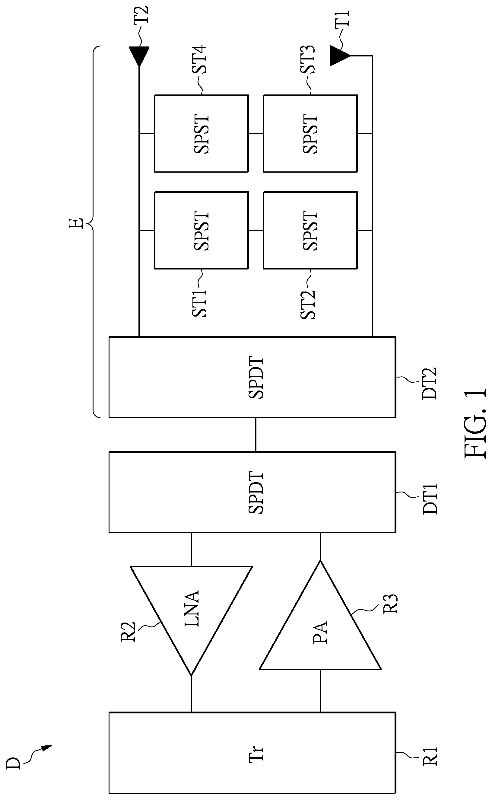
is a schematic view of a wireless communication device according to the present disclosure;
is a schematic view of an antenna matching circuit according to a first embodiment of the present disclosure;
is a schematic cross-sectional view of the antenna matching circuit according to the present disclosure;
is a schematic view of a radiation pattern of the antenna matching circuit according to the first embodiment of the present disclosure;
is a diagram showing an axial ratio of the radiation pattern of the antenna matching circuit according to the first embodiment of the present disclosure; and
is a schematic view of the antenna matching circuit according to a second embodiment of the present disclosure.
DETAILED DESCRIPTION OF THE EXEMPLARY EMBODIMENTS
The present disclosure is more particularly described in the following examples that are intended as illustrative only since numerous modifications and variations therein will be apparent to those skilled in the art. Like numbers in the drawings indicate like components throughout the views. As used in the description herein and throughout the claims that follow, unless the context clearly dictates otherwise, the meaning of “a”, “an”, and “the” includes plural reference, and the meaning of “in” includes “in” and “on”. Titles or subtitles can be used herein for the convenience of a reader, which shall have no influence on the scope of the present disclosure.
The terms used herein generally have their ordinary meanings in the art. In the case of conflict, the present document, including any definitions given herein, will prevail. The same thing can be expressed in more than one way. Alternative language and synonyms can be used for any term(s) discussed herein, and no special significance is to be placed upon whether a term is elaborated or discussed herein. A recital of one or more synonyms does not exclude the use of other synonyms. The use of examples anywhere in this specification including examples of any terms is illustrative only, and in no way limits the scope and meaning of the present disclosure or of any exemplified term. Likewise, the present disclosure is not limited to various embodiments given herein. Numbering terms such as “first”, “second” or “third” can be used to describe various components, signals or the like, which are for distinguishing one component/signal from another one only, and are not intended to, nor should be construed to impose any substantive limitations on the components, signals or the like.
In addition, the term “connect” or “connected” in the context of the present disclosure means that there is a physical connection between two elements, and the two elements are directly or indirectly connected. The term “couple” or “coupled” in the context of the present disclosure means that two elements are separate from each other and have no physical connection therebetween, and an electric field energy generated by one of the two elements excites an electric field energy generated by another one of the two elements.
Referring to , is a schematic view of a wireless communication device according to the present disclosure. The present disclosure provides a wireless communication device D, which includes a radio frequency transceiver R 1 , a single pole double throw (SPDT) switch DT 1 , a low noise amplifier R 2 , a power amplifier R 3 , and an antenna matching circuit E. The first SPDT switch DT 1 is connected between the radio transceiver R 1 and the antenna matching circuit E. The low noise amplifier R 2 is connected between the radio transceiver R 1 and the first SPDT switch DT 1 . The power amplifier R 3 is connected between the radio frequency transceiver R 1 and the first SPDT switch DT 1 . The antenna matching circuit E is formed by a circuit substrate 1 and a conductive metal material disposed on two opposite surfaces of the circuit substrate 1 . The antenna matching circuit E is operable for an operating frequency that, for example, ranges from 2.4 GHz to 2.5 GHz, and the antenna matching circuit E can be used to generate a lowest operating frequency within said range. According to an initial wavelength of the lowest operating frequency in vacuum and a dielectric coefficient of the circuit substrate 1 , a wavelength λ can be calculated by the following relationship. λ=λ c /(ε r ) 1/2 .
Here, λ e is the initial wavelength, and ε r is the dielectric coefficient of the circuit substrate 1 .
The radio frequency transceiver R 1 can transmit an output signal. The output signal passes through the power amplifier R 3 and the first SPDT switch DT 1 , and then is output from the antenna matching circuit E. On the other hand, the antenna matching circuit E can also receive an input signal. The input signal passes through the first SPDT switch DT 1 and the low noise amplifier R 2 , and then enters into the radio frequency transceiver R 1 .
First Embodiment
Referring to and , is a schematic view of an antenna matching circuit according to a first embodiment of the present disclosure. The antenna matching circuit E provided in a first embodiment of the present disclosure includes a second SPDT switch DT 2 , a first antenna element T 1 , a second antenna element T 2 , a first transmission path P 1 , a second transmission path P 2 , and a plurality of single pole single throw (SPST) switches. The second SPDT switch DT 2 is connected to the first SPDT switch DT 1 . The first antenna element T 1 and the second antenna element T 2 are connected to the second SPDT switch DT 2 . The first transmission path P 1 is connected between the first antenna element T 1 and the second SPDT switch DT 2 . The second transmission path P 2 is connected between the second antenna element T 2 and the second SPDT switch DT 2 . The SPST switches are connected between the first transmission path P 1 and the second transmission path P 2 .
The first transmission path P 1 includes a first section P 11 , a second section P 12 , and a third section P 13 . The first section P 11 is connected to the second SPDT switch DT 2 , the third section P 13 is connected to the first antenna element T 1 , and the second section P 12 is connected between the first section P 11 and the third section P 13 . The second section P 12 intersects with the first section P 11 at a first connection point S 1 , and the second section P 12 intersects with the third section P 13 at a second connection point S 2 . The second transmission path P 2 includes a fourth section P 21 , a fifth section P 22 , and a sixth section P 23 . The fourth section P 21 is connected to the second SPDT switch DT 2 . The sixth section P 23 is connected to the second antenna element T 2 . The fifth section P 22 is connected between the fourth section P 21 and the sixth section P 23 . The fifth section P 22 intersects with the fourth section P 21 at a third connection point S 3 . The fifth section P 22 intersects with the sixth section P 23 at a fourth connection point S 4 .
The antenna matching circuit E further includes a third transmission path P 3 , a fourth transmission path P 4 , and a fifth transmission path P 5 . The third transmission path P 3 is connected between the first connection point S 1 and the third connection point S 3 . The fourth transmission path P 4 is connected between the second connection point S 2 and the fourth connection point S 4 . The fifth transmission path P 5 is connected between the second SPDT switch DT 2 and the first SPDT switch DT 1 .
Reference is further made to . In the present disclosure, the SPST switches include a first SPST switch ST 1 , a second SPST switch ST 2 , a third SPST switch ST 3 , and a fourth SPST switch ST 4 . The first SPST switch ST 1 and the second SPST switch ST 2 are connected in series in the third transmission path P 3 , and the third SPST switch ST 3 and the fourth SPST switch ST 4 are connected in series in the fourth transmission path P 4 . It is worth mentioning that the first SPST switch ST 1 is adjacent to the third connection point S 3 , the second SPST switch ST 2 is adjacent to the first connection point S 1 , the third SPST switch ST 3 is adjacent to the second connection point S 2 , and the fourth SPST switch ST 4 is adjacent to the fourth connection point S 4 . Therefore, the four SPST switches are arranged to be adjacent to the first connection point S 1 , the second connection point S 2 , the third connection point S 3 , and the fourth connection point S 4 , respectively, so as to prevent generation of a stub.
Moreover, the antenna matching circuit E further includes a plurality of capacitors C. The second SPDT switch DT 2 , the first SPST switch ST 1 , the second SPST switch ST 2 , the third SPST switch ST 3 , and the fourth SPST switch ST 4 include a plurality of terminals, and the capacitors C are respectively the terminals. Since the second SPDT switch DT 2 , the first SPST switch ST 1 , the second SPST switch ST 2 , the third SPST switch ST 3 , and the fourth SPST switch ST 4 all have direct current (DC) characteristics (i.e., a DC signal may pass through each switch during an operation process thereof), the capacitors C can be connected in series to the terminals of the second SPDT switch DT 2 and the SPST switches (ST 1 to ST 4 ) as a DC block. In this way, it can be ensured that no DC signal flows into the antenna matching circuit E.
In addition, the three capacitors C connected in series to the three terminals of the second SPDT switch DT 2 can be further defined as a first capacitor C 1 , a second capacitor C 2 , and a third capacitor C 3 . The first capacitor C 1 is connected in series between the second SPDT switch DT 2 and the first section P 11 , the second capacitor C 2 is connected in series between the second SPDT switch DT 2 and the fourth section P 21 , and the third capacitor C 3 is connected in series between the second SPDT switch DT 2 and the fifth transmission path P 5 . A length of the first section P 11 (i.e., a length between the first capacitor C 1 and the first connection point S 1 ) is equal to a length of the fourth section P 21 (i.e., a length between the second capacitor C 2 and the third connection point S 3 ), and an impedance value of each of the first section P 11 and the fourth section P 21 is about 50 ohm.
As shown in , the second section P 12 , the fourth transmission path P 4 , the fifth section P 22 , and the third transmission path P 3 jointly form a loop. The shape of the loop is not limited in the present disclosure. For example, the loop can be circular, square or rhombic. A length of the second section P 12 (i.e., a length between the first connection point S 1 and the second connection point S 2 ) and a length of the fifth section P 22 (i.e., a length between the third connection point S 3 and the fourth connection point S 4 ) are both equal to one-fourth of the wavelength (λ/4) of the operating frequency generated by the antenna matching circuit E. Lengths of the third transmission path P 3 and the fourth transmission path P 4 are both equal to one-fourth wavelength (λ/4) of the operating frequency generated by the antenna matching circuit E. By designing each of the lengths of the second section P 12 , the fourth transmission path P 4 , the fifth section P 22 , and the third transmission path P 3 to be equal to one-fourth of the wavelength (λ/4) of the operating frequency, signals that are input into the first antenna element T 1 and the second antenna element T 2 can have a path difference of one-fourth of the wavelength (λ/4), such that an isolation between the first antenna element T 1 and the second antenna element T 2 can be increased. Moreover, impedance values of the third transmission path P 3 and the fourth transmission path P 4 are greater than impedance values of the second section P 12 and the fifth section P 22 . In the first embodiment, the impedance values of the third transmission path P 3 and the fourth transmission path P 4 are both about 50 ohm, and the impedance values of the second section P 12 and the fifth section P 22 are both about 35 ohm. Therefore, when the signal transmitted by the radio frequency transceiver R 1 passes through the second SPDT switch DT 2 and reaches the first antenna element T 1 and the second antenna element T 2 through one of the transmission paths (e.g., the first section P 11 of the first transmission path P 1 ), a small part of energy of the signal can be prevented from being transmitted back to the radio frequency transceiver R 1 through another one of the transmission paths (e.g., the fourth section P 21 of the second transmission path P 2 ).
Referring to and , is a schematic cross-sectional view of the antenna matching circuit according to the present disclosure. Specifically, the circuit substrate 1 has a first surface 11 and a second surface 12 that are opposite to each other, and the multiple transmission paths (P 1 to P 5 ), the second SPDT switch DT 2 , and the multiple SPST switches (ST 1 to ST 4 ) are disposed on the first surface 11 . For example, the multiple transmission paths (P 1 to P 5 ) are transmission lines formed by metal copper foil. As shown in , a metal copper foil F is disposed on the first surface 11 and the second surface 12 of the circuit substrate 1 . The first antenna element T 1 and the second antenna element T 2 are dipole antennas formed by the metal copper foil F. The first antenna element T 1 includes a first radiating portion T 11 , a second radiating portion T 12 , a third radiating portion T 13 , and a fourth radiating portion T 14 . The first radiating portion T 11 and the second radiating portion T 12 are disposed on the first surface 11 , and the third radiating portion T 13 and the fourth radiating portion T 14 are disposed on the second surface 12 . An orthogonal projection of the first radiating portion T 11 that is projected onto the second surface 12 overlaps with an orthogonal projection of the third radiating portion T 13 that is projected onto the second surface 12 . The second antenna element T 2 includes a fifth radiating portion T 21 , a sixth radiating portion T 22 , a seventh radiating portion T 23 , and an eighth radiating portion T 24 . The fifth radiating portion T 21 and the sixth radiating portion T 22 are disposed on the first surface 11 , and the seventh radiating portion T 23 and the eighth radiating portion T 24 are disposed on the second surface 12 . An orthogonal projection of the fifth radiating portion T 21 that is projected onto the second surface 12 overlaps with an orthogonal projection of the seventh radiating portion T 23 that is projected onto the second surface 12 .
The third section P 13 intersects with the first radiating portion T 11 at a fifth connection point S 5 , and the sixth section P 23 intersects with the fifth radiating portion T 21 at a sixth connection point S 6 . A length of the third section P 13 (i.e., a length between the second connection point S 2 and the fifth connection point S 5 ) is equal to a length of the sixth section P 23 (i.e., a length between the fourth connection point S 4 and the sixth connection point S 6 ), and impedance values of the third section P 13 and the sixth section P 23 are both about 50 ohm.
In addition, the first antenna element T 1 and the second antenna element T 2 are symmetrical structures, and both have the same structural design. In the first antenna element T 1 , a length L 1 of the first radiating portion T 11 is equal to a length L 3 of the third radiating portion T 13 . A width W 3 of the third radiating portion T 13 is greater than a width W 1 of the first radiating portion T 11 . In the first embodiment, the width W 3 is three times the width W 1 . A length L 2 of the second radiating portion T 12 is equal to a length L 4 of the fourth radiating portion T 14 . In the second radiating element T 2 , a length L 5 of the fifth radiating portion T 21 is equal to a length L 7 of the seventh radiating portion T 23 . A width W 4 of the seventh radiating portion T 23 is greater than a width W 2 of the fifth radiating portion T 21 . In the first embodiment, the width W 4 is three times the width W 2 . A length L 6 of the sixth radiating portion T 22 is equal to a length L 8 of the eighth radiating portion T 24 . In addition, the length L 1 of the first radiating portion T 11 is equal to the length L 5 of the fifth radiating portion T 21 . The length L 1 and the length L 5 are about three-tenths of the wavelength (0.3λ) of the operating frequency, and impedance values of the length L 1 and the length L 5 are both about 50 ohm. The length L 2 of the second radiating portion T 12 is equal to the length L 6 of the sixth radiating portion T 22 . The length L 3 of the third radiating portion T 13 is equal to the length L 7 of the seventh radiating portion T 23 . The length L 4 of the fourth radiating portion T 14 is equal to the length L 8 of the eighth radiating portion T 24 , and the length L 4 and the length L 8 are about one-fourth of the wavelength (λ/4) of the operating frequency.
The second SPDT switch DT 2 can be switched between the first transmission path P 1 and the second transmission path P 2 , and each SPST switch can be switched between a conducting state and a non-conducting state. Therefore, the antenna matching circuit E can generate different radiation patterns with different polarization directions through switching modes of the second SPDT switch DT 2 and the multiple SPST switches (ST 1 to ST 4 ).
For example, the antenna matching circuit E has a first mode, a second mode, a third mode, and a fourth mode. The radio frequency transceiver R 1 can sequentially transmit a signal to a to-be-detected object through the first mode, the second mode, the third mode and the fourth mode. Moreover, according to signal strengths measured in these modes, the radio frequency transceiver R 1 further selects the one mode that has a maximum signal strength for signal connection. When the antenna matching circuit E is switched to the first mode, the second SPDT switch DT 2 is switched to the first transmission path P 1 , the SPST switches (ST 1 to ST 4 ) are in the non-conducting states, and the first antenna element T 1 is used to generate a first radiation pattern. When the antenna matching circuit E is switched to the second mode, the second SPDT switch DT 2 is switched to the second transmission path P 2 , the SPST switches (ST 1 to ST 4 ) are in the non-conducting states, and the second antenna element T 2 is used to generate a second radiation pattern. The first radiation pattern has a first polarization direction, and the second radiation pattern has a second polarization direction. In the first embodiment, the antenna matching circuit E shown in is configured to be vertical to the ground (not shown in the figures), and the second radiation portion T 12 and the fourth radiation portion T 14 of the first antenna element T 1 are vertical to the ground. Therefore, the first polarization direction generated by the first antenna element T 1 is a vertical polarization direction. On the other hand, the sixth radiation portion T 22 and the eighth radiation portion T 24 of the second antenna element T 2 are parallel to the ground, so that the second polarization direction generated by the second antenna element T 2 is a horizontal polarization direction. The first polarization direction is orthogonal to the second polarization direction.
When the antenna matching circuit E is switched to the third mode, the second SPDT switch DT 2 is switched to the first transmission path P 1 , and the SPST switches (ST 1 to ST 4 ) are in the conducting states. When a first signal transmitted by the radio frequency transceiver R 1 is input into the fifth transmission path P 5 and passes through the first transmission path P 1 , the first signal travels around the second section P 12 , the fourth transmission path P 4 , the fifth section P 22 , and the third transmission path P 3 along a counterclockwise direction. Therefore, one part of energy of the first signal will be transmitted to the first antenna element T 1 , and then another part of the energy of the first signal will be transmitted to the second antenna element T 2 . Accordingly, the first antenna element T 1 and the second antenna element T 2 can generate a third radiation pattern with a third polarization direction, and the third polarization direction is a right-hand circular polarization (RHCP) direction.
When the antenna matching circuit E is switched to the fourth mode, the second SPDT switch DT 2 is switched to the second transmission path P 2 , and the SPST switches (ST 1 to ST 4 ) are in the conducting states. When a second signal transmitted by the radio frequency transceiver R 1 is input into the fifth transmission path P 5 and passes through the second transmission path P 2 , the second signal travels around the fifth section P 22 , the fourth transmission path P 4 , the second section P 12 , and the third transmission path P 3 along a clockwise direction. Therefore, one part of energy of the second signal will be transmitted to the second antenna element T 2 , and then another part of the energy of the second signal will be transmitted to the first antenna element T 1 . Accordingly, the first antenna element T 1 and the second antenna element T 2 are used to generate a fourth radiation pattern with a fourth polarization direction, and the fourth polarization direction is a left-hand circular polarization (LHCP) direction.
Referring to and , is a schematic view of a radiation pattern of the antenna matching circuit according to the first embodiment of the present disclosure, and is a diagram showing an axial ratio of the radiation pattern of the antenna matching circuit according to the first embodiment of the present disclosure. The third mode of the antenna matching circuit E is exemplified in for illustrative purposes. As shown in , the first antenna element T 1 generates a radiation pattern of a vertical component, the second antenna element T 2 generates a radiation pattern of a horizontal component, and an axial ratio diagram converted from the two radiation patterns is shown in . As shown in , an angular range where the axial ratio is less than 5 (the axial ratio of an ideal circular polarized antenna is 1) is about 240 degrees. In other words, in , the two radiation patterns have the same radiation energy (the horizontal component and the vertical component of the ideal circular polarized antenna have the same radiation energy), and the angular range is about 240 degrees. Therefore, the radiation pattern generated by the first antenna element T 1 and the second antenna element T 2 can have a circular polarization effect.
Second Embodiment
Referring to , is a schematic view of the antenna matching circuit according to a second embodiment of the present disclosure. In the second embodiment, the first antenna element T 1 and the second antenna element T 2 are slot antennas. The first transmission path P 1 further includes a seventh section P 14 , and the second transmission path P 2 further includes an eighth section P 24 . An aspect ratio of the seventh section P 14 and the eighth section P 24 is about 2. The seventh section P 14 intersects with the third section P 13 at a seventh connection point S 7 , and the eighth section P 24 intersects with the sixth section P 23 at an eighth connection point S 8 . The first antenna element T 1 includes a first slot T 10 , the second antenna element T 2 includes a second slot T 20 , and the first slot T 10 and the second slot T 20 are formed on the metal copper foil F that is disposed on the second surface 12 of the circuit substrate 1 . A length HL 1 of the first slot T 10 is equal to a length HL 2 of the second slot T 20 . An orthogonal projection of the seventh section P 14 that is projected onto the second surface 12 partially overlaps with an orthogonal projection of the first slot T 10 that is projected onto the second surface 12 . That is to say, the seventh section P 14 crosses over the first slot T 10 , and a length L 9 of the seventh section P 14 is greater than a width HW 1 of the first slot T 10 . An orthogonal projection of the eighth section P 24 that is projected onto the second surface 12 partially overlaps with an orthogonal projection of the second slot T 20 that is projected onto the second surface 12 . That is to say, the eighth section P 24 crosses over the second slot T 20 , and a length L 10 of the eighth section P 24 is greater than a width HW 2 of the second slot T 20 . In addition, the length HL 1 of the first slot T 10 and the length HL 2 of the second slot T 20 are both about one-half of the wavelength (λ/2) of the operating frequency.
Beneficial Effects of the Embodiments
In conclusion, in the wireless communication device D and the antenna matching circuit E provided by the present disclosure, by virtue of “in response to the antenna matching circuit E being switched to a first mode, the second SPDT switch DT 2 is switched to the first transmission path P 1 , the SPST switches (ST 1 to ST 4 ) are in non-conducting states, and the first antenna element T 1 is used to generate a first radiation pattern,” “in response to the antenna matching circuit E being switched to a second mode, the second SPDT switch DT 2 is switched to the second transmission path P 2 , the SPST switches (ST 1 to ST 4 ) are in the non-conducting states, and the second antenna element T 2 is used to generate a second radiation pattern,” and “the first radiation pattern having a first polarization direction, the second radiation pattern having a second polarization direction, and the first polarization direction being orthogonal to the second polarization direction,” a polarization direction of an antenna can be changed with different environments for improving a signal receiving capability.
Moreover, the antenna matching circuit E has a first mode, a second mode, a third mode, and a fourth mode. When the antenna matching circuit E is switched to the first mode, the second SPDT switch DT 2 is switched to the first transmission path P 1 , and the SPST switches (ST 1 to ST 4 ) are in the non-conducting states. When the antenna matching circuit E is switched to the second mode, the second SPDT switch DT 2 is switched to the second transmission path P 2 , and the SPST switches (ST 1 to ST 4 ) are in the non-conducting states. When the antenna matching circuit E is switched to the third mode, the second SPDT switch DT 2 is switched to the first transmission path P 1 , and the SPST switches (ST 1 to ST 4 ) are in conducting states. When the antenna matching circuit E is switched to the fourth mode, the second SPDT switch DT 2 is switched to the second transmission path P 2 , and the SPST switches (ST 1 to ST 4 ) are in the conducting states. Accordingly, the antenna matching circuit E can generate various polarization directions (e.g., a horizontal polarization direction, a vertical polarization direction, a right-hand circular polarization direction, and a left-hand circular polarization direction) by switching different modes, such that a user does not need to specifically adjust an antenna position for obtaining an improved signal receiving capability.
The foregoing description of the exemplary embodiments of the disclosure has been presented only for the purposes of illustration and description and is not intended to be exhaustive or to limit the disclosure to the precise forms disclosed. Many modifications and variations are possible in light of the above teaching.
The embodiments were chosen and described in order to explain the principles of the disclosure and their practical application so as to enable others skilled in the art to utilize the disclosure and various embodiments and with various modifications as are suited to the particular use contemplated. Alternative embodiments will become apparent to those skilled in the art to which the present disclosure pertains without departing from its spirit and scope.
Figures (6)
Citations
This patent cites (11)
- US10361490
- US2017/0230074
- US2018/0034624
- US2022/0291395
- US2023/0420845
- US2025/0047341
- US103597659
- US111293429
- US114760378
- USM537317
- USWO-2023167785