Semiconductor Chip with Fuse Structure in Scribe Lane and Method of Fabricating the Same
Abstract
Disclosed is a method of designing and fabricating a semiconductor chip including a fuse cell. The method may include preparing a semiconductor chip layout, the semiconductor chip layout including a main chip layout and a scribe lane layout enclosing the main chip layout; disposing a fuse layout in the scribe lane layout; setting the main chip layout as a first data preparation region; setting the scribe lane layout and the fuse layout as a second data preparation region; obtaining a first resulting structure and a second resulting structure, respectively, by performing a data preparation process on the first and second data preparation regions; merging the first and second resulting structures to generate mask data; manufacturing a photomask, based on the mask data; and forming semiconductor chips on a wafer using the photomask.
Claims (20)
1. A method of fabricating a semiconductor chip, comprising: preparing a semiconductor chip layout, the semiconductor chip layout comprising a main chip layout and a scribe lane layout enclosing the main chip layout; disposing a fuse layout in the scribe lane layout, the fuse layout not being in the main chip layout; setting the main chip layout as a first data preparation region; setting the scribe lane layout and the fuse layout as a second data preparation region; obtaining a first resulting structure and a second resulting structure, respectively, by performing a data preparation process on the first data preparation region and the second data preparation region; merging the first resulting structure and the second resulting structure to generate mask data; manufacturing a photomask based on the mask data; and forming semiconductor chips on a wafer using the photomask.
11. A method of fabricating a semiconductor chip, comprising: forming semiconductor chips on a wafer, each of the semiconductor chips comprising a main chip including a first portion of a connection structure, a scribe lane on a first boundary of the main chip, and a fuse cell in the scribe lane, the fuse cell including a fuse structure and a second portion of the connection structure, the connection structure extending from the fuse structure into the main chip; testing functional elements in the main chip through the fuse cell, the fuse cell not being in the main chip; and dicing the wafer to separate the semiconductor chips from each other to provide a plurality of separated semiconductor chips, the dicing the wafer including removing the fuse structure, and each separated semiconductor chip of the plurality of separated semiconductor chips including a cut portion of the connection structure.
16. A semiconductor chip, comprising: a main chip; a cut scribe lane on a first boundary of the main chip; a cut fuse cell in the cut scribe lane, the cut fuse cell not being in the main chip; and a connection structure extending from the cut fuse cell into the main chip, the main chip including first dummy structures disposed around the connection structure, the cut fuse cell including second dummy structures disposed around the connection structure, the main chip and the cut fuse cell defining a dummy-free region between the first dummy structures and the second dummy structures, and the dummy-free region overlapping the first boundary.
Show 17 dependent claims
2. The method of claim 1 , wherein the fuse layout is adjacent to a first boundary of the main chip layout, the main chip layout comprises a first portion of a connection pattern, the fuse layout comprises a fuse pattern and a second portion of the connection pattern, and the connection pattern extends from the fuse pattern into the main chip layout, wherein an entirety of the fuse pattern is in the fuse layout.
3. The method of claim 2 , wherein the data preparation process on the first data preparation region comprises generating first dummy patterns in the main chip layout, and the first dummy patterns are generated around the first portion of the connection pattern and are spaced apart from the first boundary.
4. The method of claim 3 , wherein the data preparation process on the second data preparation region comprises generating second dummy patterns in the fuse layout, the second dummy patterns are generated around the fuse pattern and the second portion of the connection pattern, and the second dummy patterns are spaced apart from the first boundary.
5. The method of claim 4 , wherein the mask data comprises a dummy-free region between the first dummy patterns and the second dummy patterns, and the first boundary overlaps the dummy-free region.
6. The method of claim 2 , wherein the first resulting structure includes the first portion of the connection pattern, the second resulting structure includes the second portion of the connection pattern, and the merging the first resulting structure and the second resulting structure comprises aligning the second portion of the connection pattern of the first resulting structure to the first portion of the connection pattern of the second resulting structure.
7. The method of claim 1 , wherein the data preparation process on the second data preparation region comprises: performing a first Optical Proximity Correction process on the scribe lane layout; and performing a second Optical Proximity Correction process on the fuse layout, wherein the first Optical Proximity Correction process and the second Optical Proximity Correction process have Optical Proximity Correction rules that are different from each other.
8. The method of claim 7 , wherein the second Optical Proximity Correction process has a same Optical Proximity Correction rule as an Optical Proximity Correction process performed on the first data preparation region.
9. The method of claim 1 , further comprising: testing functional elements in a main chip, wherein each of the semiconductor chips comprises the main chip and a fuse cell, the fuse cell is adjacent to a first boundary of the main chip, and the testing the functional elements in the main chip is performed through the fuse cell.
10. The method of claim 9 , further comprising: performing a dicing process on the wafer to separate the semiconductor chips from each other, wherein the fuse cell of each of the semiconductor chips is cut by the dicing process.
12. The method of claim 11 , wherein the main chip comprises first dummy structures disposed around the first portion of the connection structure, the fuse cell comprises second dummy structures disposed around the second portion of the connection structure, the first dummy structures and the second dummy structures are spaced apart from the first boundary such that the main chip and the fuse cell define a dummy-free region between the first dummy structure and the second dummy structure, and the dummy-free region overlaps the first boundary.
13. The method of claim 12 , wherein, after the dicing the wafer, some of the second dummy structures are left in a cut portion of the fuse cell.
14. The method of claim 12 , wherein a separated semiconductor chip is among the plurality of separated semiconductor chips and comprises a cut portion of the scribe lane and a cut portion of the fuse cell, the cut portion of the fuse cell is in the cut portion of the scribe lane, at least one of the second dummy structures is in the cut portion of the fuse cell and in an edge of the separated semiconductor chip, the edge of the separated semiconductor chip includes a cut supplementary structure in the cut portion of the scribe lane.
15. The method of claim 11 , wherein the fuse structure is configured to be programmed with a code.
17. The semiconductor chip of claim 16 , wherein the main chip comprises a plurality of functional elements, and each of the plurality of functional elements comprises a memory block, an analog logic block, an input/output (I/O) logic block, a central processing unit (CPU) block, or a radio frequency block.
18. The semiconductor chip of claim 17 , wherein the connection structure is electrically connected to at least one of the plurality of functional elements.
19. The semiconductor chip of claim 16 , wherein the cut scribe lane comprises a cut supplementary structure, at least one of the second dummy structures is disposed in an edge of the semiconductor chip, and the cut supplementary structure is disposed in the edge.
20. The semiconductor chip of claim 16 , wherein a fuse structure, which is configured to be programmed with a code, is excluded from the cut fuse cell.
Full Description
Show full text →
CROSS-REFERENCE TO RELATED APPLICATIONS
This U.S. non-provisional patent application claims priority under 35 U.S.C. § 119 to Korean Patent Application No. 10-2021-0170933, filed on Dec. 2, 2021 in the Korean Intellectual Property Office, the entire contents of which are hereby incorporated by reference.
BACKGROUND
The present disclosure relates to a method of designing and fabricating a semiconductor chip including a fuse cell.
Due to their small-sized, multifunctional, and/or low-cost characteristics, semiconductor devices are being esteemed as important elements in the electronics industry. The semiconductor devices are classified into a semiconductor memory device for storing data, a semiconductor logic device for processing data, and a hybrid semiconductor device including both memory and logic elements. As the electronic industry advances, there may be more demand for semiconductor devices with improved characteristics. For example, there may be more demand for semiconductor devices with high reliability, high performance, and/or multiple functions. To meet this demand, structural complexity and/or integration density of semiconductor devices are being increased.
SUMMARY
An embodiment of inventive concepts provides a method of fabricating a semiconductor chip with improved security.
An embodiment of inventive concepts provides a method of increasing the number of net dies formed on a wafer, when a semiconductor chip is fabricated.
According to an embodiment of inventive concepts, a method of fabricating a semiconductor chip may include preparing a semiconductor chip layout, the semiconductor chip layout including a main chip layout and a scribe lane layout enclosing the main chip layout; disposing a fuse layout in the scribe lane layout; setting the main chip layout as a first data preparation region; setting the scribe lane layout and the fuse layout as a second data preparation region; obtaining a first resulting structure and a second resulting structure, respectively, by performing a data preparation process on the first data preparation region and the second data preparation region; merging the first resulting structure and the second resulting structure to generate mask data; manufacturing a photomask, based on the mask data; and forming semiconductor chips on a wafer using the photomask.
According to an embodiment of inventive concepts, a method of fabricating a semiconductor chip may include forming semiconductor chips on a wafer, each of the semiconductor chips including a main chip including a first portion of a connection structure, a scribe lane on a first boundary of the main chip, and a fuse cell in the scribe lane; testing functional elements in the main chip through the fuse cell; and dicing the wafer to separate the semiconductor chips from each other to provide a plurality of a separated semiconductor chips. The fuse cell may include a fuse structure and a second portion of a connection structure. The connection structure may extend from the fuse structure into the main chip. The dicing the wafer may include removing the fuse structure. Each separated semiconductor chip among the plurality of separated semiconductor chips may include a cut portion of the connection structure.
According to an embodiment of inventive concepts, a semiconductor chip may include a main chip; a cut scribe lane on a first boundary of the main chip; a cut fuse cell in the cut scribe lane; and a connection structure extending from the cut fuse cell into the main chip. The main chip may include first dummy structures disposed around the connection structure. The cut fuse cell may include second dummy structures disposed around the connection structure. The main chip and the cut fuse cell may define a dummy-free region between the first dummy structures and the second dummy structures. The dummy-free region may overlap the first boundary.
BRIEF DESCRIPTION OF THE DRAWINGS
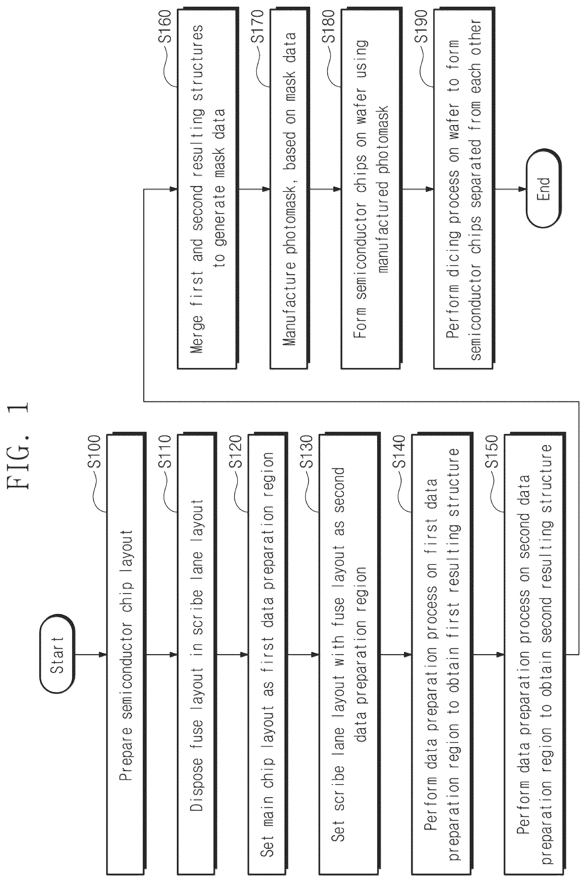
is a flow chart illustrating a method of designing and fabricating a semiconductor chip according to an embodiment of inventive concepts.
are schematic diagrams, each of which illustrates a semiconductor chip layout according to an embodiment of inventive concepts.
is an enlarged plan view illustrating a portion ‘M’ of .
to 11 are schematic diagrams illustrating a method of performing a data preparation process on the layout of .
is a plan view illustrating semiconductor chips, which are formed on a wafer, according to an embodiment of inventive concepts.
is an enlarged plan view illustrating a portion ‘M’ of .
A and 14 B illustrate a fuse cell according to an embodiment of inventive concepts, A illustrates a circuit diagram of an electrical fuse (e-fuse), and B illustrates a structure of the e-fuse.
is a plan view illustrating a semiconductor chip, which is cut by dicing the wafer of .
is an enlarged plan view illustrating a portion ‘M’ of .
is a schematic diagram illustrating a semiconductor chip layout according to a comparative example.
is a plan view illustrating semiconductor chips, which are formed on a wafer based on the layout of .
DETAILED DESCRIPTION
When the terms “about” or “substantially” are used in this specification in connection with a numerical value, it is intended that the associated numerical value includes a manufacturing or operational tolerance (e.g., ±10%) around the stated numerical value. Moreover, when the words “generally” and “substantially” are used in connection with geometric shapes, it is intended that precision of the geometric shape is not required but that latitude for the shape is within the scope of the disclosure. Further, regardless of whether numerical values or shapes are modified as “about” or “substantially,” it will be understood that these values and shapes should be construed as including a manufacturing or operational tolerance (e.g., ±10%) around the stated numerical values or shapes.
Example embodiments of inventive concepts will now be described more fully with reference to the accompanying drawings, in which example embodiments are shown.
is a flow chart illustrating a method of designing and fabricating a semiconductor chip according to an embodiment of inventive concepts. to 16 are schematic diagrams illustrating the designing and fabricating method of . For example, the semiconductor chip according to the present embodiment may include a Micro Computing Unit (MCU).
are schematic diagrams, each of which illustrates a semiconductor chip layout according to an embodiment of inventive concepts. Referring to , a semiconductor chip layout including a main chip layout MCL may be prepared (in S 100 ). For example, the main chip layout MCL may be a graphic data system (GDS) layout that is a file provided in the form of the GDS file format. In an embodiment, the semiconductor chip layout may include a scribe lane layout SLL, in addition to the main chip layout MCL.
The main chip layout MCL may include a plurality of functional element layouts FEL 1 -FEL 5 . For example, the main chip layout MCL may include first to fifth functional element layouts FEL 1 -FEL 5 . The first to fifth functional element layouts FEL 1 -FEL 5 may constitute an integrated circuit of a semiconductor chip.
Each of the first to fifth functional element layouts FEL 1 -FEL 5 may be a functional block constituting the integrated circuit. Each of the first to fifth functional element layouts FEL 1 -FEL 5 may include one of a memory block, an analog logic block, an input/output (I/O) logic block, a central processing unit (CPU) block, and a radio frequency block.
The main chip layout MCL may be rectangular. The main chip layout MCL may include first to fourth boundaries CBL 1 -CBL 4 , which correspond to respective four sides of the rectangular main chip layout MCL. The first and second boundaries CBL 1 and CBL 2 may be parallel to a second direction D 2 and may be opposite to each other in a first direction D 1 . The third and fourth boundaries CBL 3 and CBL 4 may be parallel to the first direction D 1 and may be opposite to each other in the second direction D 2 .
The scribe lane layout SLL may be provided to enclose the main chip layout MCL. The first to fourth boundaries CBL 1 -CBL 4 may be defined between the scribe lane layout SLL and the main chip layout MCL. The scribe lane layout SLL may be adjacent to the first to fourth boundaries CBL 1 -CBL 4 of the main chip layout MCL. The scribe lane layout SLL may include a test element group (TEG) pattern and a key pattern.
A width of the scribe lane layout SLL in the first direction D 1 may be a first length LI 1 . A width of the scribe lane layout SLL in the second direction D 2 may be a second length LI 2 . The first length LI 1 and the second length LI 2 may be equal to or different from each other.
In an embodiment, the preparing of the semiconductor chip layout may include a layout design process. In detail, the layout design process may be performed to realize a logically-complete integrated circuit on a silicon wafer. For example, the layout design process may be performed, based on the schematic circuit prepared in the high-level design process or the corresponding netlist. The layout design process may include a routing operation of placing and connecting various standard cells that are provided from a cell library, based on a desired and/or alternatively predetermined design rule.
After the routing operation, a verification operation may be performed on the layout to check whether there is a portion violating the given design rule. In an embodiment, the verification operation may include evaluating verification items, such as a design rule check (DRC), an electronical rule check (ERC), and a layout vs schematic (LVS). The evaluating of the DRC item may be performed to evaluate whether the layout meets the given design rule. The evaluating of the ERC item may be performed to evaluate whether there is an issue of electrical disconnection in the layout. The evaluating of the LVS item may be performed to evaluate whether the layout is prepared to coincide with the gate-level netlist.
In another embodiment, the semiconductor chip layout may be provided from a designer. The method according to an embodiment of inventive concepts may include operations which are performed to actually realize a semiconductor chip on a wafer, based on the semiconductor chip layout provided from the designer.
Referring to , a fuse layout EFL may be disposed in the scribe lane layout SLL (in S 110 ). For example, the fuse layout EFL may be disposed adjacent to the first boundary CBL 1 of the main chip layout MCL. The fuse layout EFL may be disposed in a portion of the scribe lane layout SLL adjacent to the first boundary CBL 1 .
According to an embodiment of inventive concepts, although the fuse layout EFL is disposed in the scribe lane layout SLL, a width of the scribe lane layout SLL may not be changed. In other words, the first length LIL in the first direction D 1 , of the scribe lane layout SLL of may be equal to the first length LIL in the first direction D 1 , of the scribe lane layout SLL of .
The fuse layout EFL may include a programmable device, in which a code can be input. For example, the fuse layout EFL may include an electrical fuse (e-fuse). Although the fuse layout EFL is disposed in the scribe lane layout SLL, the fuse layout EFL may be connected to the main chip layout MCL.
In a comparative example, the fuse layout EFL may be disposed in the main chip layout MCL. A fuse structure, which is formed based on the fuse layout EFL, may be used when a semiconductor chip formed on a wafer is tested. In the case where the fuse layout EFL is disposed in the main chip layout MCL, the fuse structure may be left in a final structure of the semiconductor chip. In this case, a security problem may occur, because the fuse structure contains the designer's code as it is.
By contrast, according to an embodiment of inventive concepts, the fuse layout EFL may be disposed in the scribe lane layout SLL. A fuse structure, which is formed based on the fuse layout EFL, may be removed when a wafer dicing process is performed on the scribe lane. Accordingly, the fuse structure, in which the designer's code is stored, may not exist in the final structure of the semiconductor chip. Thus, it may be possible to limit and/or prevent the security issue from occurring in a semiconductor chip or to improve a security property of the semiconductor chip.
is an enlarged plan view illustrating a portion ‘M’ of . illustrates a layout of a specific layer in the semiconductor chip layout. For example, illustrates a layout of an FEOL layer of the semiconductor chip.
The scribe lane layout SLL may include a first scribe lane layout SLL 1 and a second scribe lane layout SLL 2 , which are respectively placed at opposite ends of the fuse layout EFL and the fuse layout EFL. The first scribe lane layout SLL 1 may include a first supplementary pattern SP 1 , and the second scribe lane layout SLL 2 may include a second supplementary pattern SP 2 . Each of the first and second supplementary patterns SP 1 and SP 2 may be a TEG pattern or a key pattern.
The fuse layout EFL may include a fuse pattern EFP and connection patterns CNP, which are extended from the fuse pattern EFP toward the main chip layout MCL. The connection patterns CNP may extend parallel to the first direction D 1 and may have a line shape. The connection patterns CNP may be extended from the fuse layout EFL into the main chip layout MCL beyond the first boundary CBL 1 of the main chip layout MCL.
to 11 are schematic diagrams illustrating a method of performing a data preparation process on the layout of .
Referring to , the main chip layout MCL may be set as a first data preparation region DPR 1 (in S 120 ). In the data preparation process according to an embodiment of inventive concepts, a target layout should have a rectangular shape. If the target layout has a polygonal shape, an OPC rule may be applied incorrectly, and in this case, there may be a difficulty in performing the data preparation process.
In the case where the main chip layout MCL and the fuse layout EFL are set as the first data preparation region DPR 1 , a target region may have a polygonal shape, not a rectangular shape. In the case where the target region is polygonal, the data preparation process cannot be performed, and thus, it may be difficult to set the main chip layout MCL and the fuse layout EFL collectively as the first data preparation region DPR 1 .
The scribe lane layout SLL, in which the fuse layout EFL is disposed, may be set as a second data preparation region DPR 2 (in S 130 ). Since the scribe lane layout SLL including the fuse layout EFL has a rectangular shape, it may be set as the second data preparation region DPR 2 . Since the fuse layout EFL is a functional element connected to the main chip layout MCL, it may be preferable to perform the data preparation process on both of the fuse layout EFL and the main chip layout MCL. However, due to the limitation on the shape of the target region in the afore-described data preparation process, the fuse layout EFL, which is combined with not the main chip layout MCL but the scribe lane layout SLL, may be set as the second data preparation region DPR 2 .
Referring to , the data preparation process may be performed on the first data preparation region DPR 1 (in S 140 ). For example, the data preparation process may be performed on the main chip layout MCL. The data preparation process on the first data preparation region DPR 1 may include performing an optical proximity correction (OPC) process and performing a mask data preparation (MDP) process.
First, the optical proximity correction (OPC) process may be performed on the first data preparation region DPR 1 . Layout patterns, which are prepared by the layout design process, may be realized on a silicon wafer through a photolithography process. The OPC process may be performed to correct an optical proximity or distortion effect, which may occur in the photolithography process. That is, by performing the OPC process, it may be possible to correct optical distortion effects (e.g., refraction) or process effects, which may be caused by an optical effect during an exposure operation performed using a designed pattern. As a result of the OPC process, the shapes and positions of patterns in the designed layout may be changed or biased.
As illustrated in , the connection patterns CNP in the first data preparation region DPR 1 may be corrected through the optical proximity correction (OPC) process. For example, the shapes and/or positions of the connection pattern CNP in the main chip layout MCL may be changed. After the OPC process, a layout verification process may be performed to examine whether there is a portion violating an OPC rule and/or a mask rule.
Referring to , the mask data preparation (MDP) process may be performed on the first data preparation region DPR 1 . The MDP process may include generating first dummy patterns DMP 1 . The first dummy patterns DMP 1 may be generated in the first data preparation region DPR 1 . The first dummy patterns DMP 1 may be generated in an empty region, in which the connection patterns CNP are absent. Since the first dummy patterns DMP 1 fill the empty region, it may be possible to improve uniformity of a pattern density. For example, since the uniformity of the pattern density is improved, it may be possible to limit and/or prevent a process defect caused by an optical distortion effect.
The first dummy patterns DMP 1 may not be generated in a region adjacent to a boundary of the first data preparation region DPR 1 . For example, the first dummy patterns DMP 1 may not be generated in a region of the main chip layout MCL, which is disposed adjacent to the first boundary CBL 1 . A first separation distance SED 1 may be defined between the first boundary CBL 1 and the first dummy pattern DMP 1 , which is most adjacent to the first boundary CBL 1 . The first separation distance SED 1 may be larger than a pitch between the first dummy patterns DMP 1 .
After the MDP process, a layout verification process may be performed to examine whether there is a portion violating a mask rule. For example, a mask rule check MRC may be performed, after the MDP process. After the data preparation process, the first data preparation region DPR 1 of may be output as a first resulting structure (in S 140 ).
Referring to , a data preparation process may be performed on the second data preparation region DPR 2 (in S 150 ). The data preparation process on the second data preparation region DPR 2 may be performed in a manner that is different and distinct from the data preparation process on the first data preparation region DPR 1 described above.
First, an optical proximity correction (OPC) process may be performed on the first and second scribe lane layouts SLL 1 and SLL 2 of the second data preparation region DPR 2 . An OPC rule for the first and second scribe lane layouts SLL 1 and SLL 2 may be different from an OPC rule for the fuse layout EFL. Thus, the optical proximity correction (OPC) process may be performed on only the first and second scribe lane layouts SLL 1 and SLL 2 , not on the fuse layout EFL.
As illustrated in , the first and second supplementary patterns SP 1 and SP 2 in the second data preparation region DPR 2 may be corrected through the optical proximity correction (OPC) process. For example, the shapes and/or positions of the first and second supplementary patterns SP 1 and SP 2 in the first and second scribe lane layouts SLL 1 and SLL 2 may be changed. Next, an OPC rule check (ORC) process may be performed.
Referring to , an optical proximity correction process may be performed on the fuse layout EFL of the second data preparation region DPR 2 . An OPC rule for the fuse layout EFL may be the same as an OPC rule for the main chip layout MCL. As illustrated in , the fuse pattern EFP and the connection patterns CNP in the second data preparation region DPR 2 may be corrected through the OPC process. For example, the shapes and/or positions of the connection patterns CNP in the fuse layout EFL may be changed. Thereafter, the OPC rule check (ORC) process may be performed.
Referring to , a mask data preparation process may be performed on the fuse layout EFL of the second data preparation region DPR 2 . The MDP process may include generating second dummy patterns DMP 2 . The second dummy patterns DMP 2 may be generated in the fuse layout EFL of the second data preparation region DPR 2 . Although not shown, dummy patterns may be generated in the first and second scribe lane layouts SLL 1 and SLL 2 .
The second dummy patterns DMP 2 may be generated in an empty region, in which the fuse pattern EFP and the connection patterns CNP are absent. Since the second dummy patterns DMP 2 fill the empty region, it may be possible to improve uniformity of a pattern density.
The second dummy patterns DMP 2 may not be generated adjacent to a boundary of the second data preparation region DPR 2 . For example, the second dummy patterns DMP 2 may not be generated in a region that is adjacent to the first boundary CBL 1 of the main chip layout MCL. A second separation distance SED 2 may be defined between the first boundary CBL 1 and the second dummy pattern DMP 2 most adjacent thereto. The second separation distance SED 2 may be larger than a pitch between the second dummy patterns DMP 2 . The second separation distance SED 2 may be equal to or different from the first separation distance SED 1 of .
After the MDP process, a layout verification process may be performed to examine whether there is a portion violating a mask rule. For example, a mask rule check may be performed, after the MDP process. After the data preparation process, the second data preparation region DPR 2 of may be output as a second resulting structure (in S 150 ).
Referring to , the first resulting structure of and the second resulting structure of may be merged to generate a mask data for generating a mask (in S 160 ). The merging of the first and second resulting structures may include matching the first boundary CBL 1 of the first resulting structure with the first boundary CBL 1 of the second resulting structure and aligning the connection patterns CNP of the first resulting structure to the connection patterns CNP of the second resulting structure. Since the connection patterns CNP of the first resulting structure are aligned to the connection patterns CNP of the second resulting structure, the connection patterns CNP may be generated to continuously extend from the fuse pattern EFP into the main chip layout MCL.
As shown in the mask data of , a dummy-free region DFR may be generated on the first boundary CBL 1 . The dummy-free region DFR may be defined between the first dummy pattern DMP 1 and the second dummy pattern DMP 2 . The dummy-free region DFR may be overlapped with the first boundary CBL 1 . Since there is no dummy pattern in the dummy-free region DFR, the dummy-free region DFR may be an empty region. A length in the first direction D 1 of the dummy-free region DFR may be equal to a sum of the first and second separation distances SED 1 and SED 2 .
The dummy-free region DFR may be generated by performing an additional data preparation process on each of the main chip layout MCL and the fuse layout EFL. As a comparative example, in the case where the same data preparation process is performed on the first data preparation region DPR 1 which is set by collectedly combining the main chip layout MCL and the fuse layout EFL, dummy patterns are inevitably generated in the dummy-free region DFR of .
Since the first and second resulting structures are merged, it may be possible to obtain a mask data, in which the data preparation process on the semiconductor chip layout of has been finished. A photomask may be manufactured, based on the mask data (in S 170 ).
is a plan view illustrating semiconductor chips, which are formed on a wafer, according to an embodiment of inventive concepts. is an enlarged plan view illustrating a portion ‘M’ of .
Referring to , semiconductor chips may be formed on a wafer W using a manufactured photomask (in S 180 ). In the actual fabricating process using the photomask, various exposing and etching operations may be repeatedly performed. As a result of these operations, various patterns, which have shapes defined by the layout design process, may be sequentially formed on the wafer W. Each of the semiconductor chips on the wafer W may include a main chip MC and a scribe lane SL, which is provided around the main chips MC.
The main chips MC may be two-dimensionally arranged on the wafer W. The scribe lane SL may be provided between the main chips MC. Each of the main chips MC may include at least one fuse cell EF, which is adjacent to a boundary thereof. The fuse cell EF may be disposed in the scribe lane SL. Each of the main chips MC may include a plurality of functional elements FE. The functional elements FE may be devices, which are formed by realizing the first to fifth functional element layouts FEL 1 -FEL 5 previously described with reference to on the wafer W.
In an embodiment, the main chips MC, which are adjacent to each other in the first direction D 1 , may be spaced apart from each other in a first distance SPD 1 . The scribe lane SL between the main chips MC, which are adjacent to each other in the first direction D 1 , may have a width WI in the first direction D 1 . The width WI of the scribe lane SL may be substantially equal to the first distance SPD 1 .
Referring to , the scribe lane SL may be adjacent to a first boundary CB 1 of the main chip MC. The scribe lane SL may include the fuse cell EF adjacent to the first boundary CB 1 , a first scribe lane SL 1 at a side of the fuse cell EF, and a second scribe lane SL 2 at an opposite side of the fuse cell EF.
The main chip MC may include first dummy structures DMS 1 , which are adjacent to the first boundary CB 1 . The fuse cell EF may include a fuse structure EFS and second dummy structures DMS 2 , which are provided around the fuse structure EFS. Connection structures CNS may be provided to extend from the fuse structure EFS into the main chip MC. At least one of the first dummy structures DMS 1 may be disposed between adjacent ones of the connection structures CNS. At least one of the second dummy structures DMS 2 may be disposed between adjacent ones of the connection structures CNS.
The first scribe lane SL 1 may include a first supplementary structure SS 1 , and the second scribe lane SL 2 may include a second supplementary structure SS 2 . Each of the first and second supplementary structures SS 1 and SS 2 may be a TEG pattern or a key pattern.
The dummy-free region DFR may be defined on the first boundary CB 1 between the main chip MC and the fuse cell EF. As previously described with reference to , the first and second dummy structures DMS 1 and DMS 2 may not exist in the dummy-free region DFR. The second dummy structure DMS 2 , which is closest to the first boundary CB 1 , may be spaced apart from the first dummy structure DMS 1 , which is closest to the first boundary CB 1 , in the first direction D 1 with the dummy-free region DFR interposed therebetween.
A pattern density of the dummy-free region DFR may be smaller than a pattern density of the main chip MC and a pattern density of the fuse cell EF. Here, the pattern density may mean the number of dummy patterns disposed within a given area. For example, a width of the dummy-free region DFR in the first direction D 1 may be larger than five times a pitch between the first dummy structures DMS 1 .
The structures shown in may be conductive patterns in the FEOL layer. The structures of (e.g., the conductive patterns of the FEOL layer) may be formed of or include at least one of doped semiconductor materials (e.g., doped polysilicon), metallic materials, or metal nitride materials.
Referring back to , the fuse cell EF may be connected to the functional elements FE, respectively, in the main chip MC through the connection structures CNS. The functional elements FE in the main chip MC may be tested through a code, which is programmed in the fuse cell EF. As a result of the test, it may be possible to examine whether or not there is a failure in each of the main chips MC.
A and 14 B illustrate a fuse cell according to an embodiment of inventive concepts, A illustrates a circuit diagram of an electrical fuse (e-fuse), and B illustrates a structure of the e-fuse.
Referring to A , a fuse driving circuit may include an e-fuse. The e-fuse may include one end, which is electrically connected to a transistor, and an opposite end, to which a specific voltage is applied.
The transistor of A may be a transistor that is provided in the functional element FE in the main chip MC of . A gate voltage Vgs may be applied to the gate of the transistor, and a ground voltage GND may be provided to one end of the transistor. In the case where the gate voltage Vgs is applied to the gate of the transistor and a voltage Vfs is applied to the opposite end of the e-fuse, the e-fuse may be blown, and in this case, a resistance value of the e-fuse may be increased. In other words, the e-fuse may be physically opened. That is, a resistance value of the e-fuse may be measured by applying the specific voltage to the opposite ends of the e-fuse, and in this case, the measured resistance value may be used to determine whether the fuse is blown. The e-fuse may be programmed by applying the specific voltage to the opposite ends of the e-fuse.
B illustrates an example of an e-fuse structure in the fuse cell EF of . The fuse structure EFS may have a three-dimensional structure. The fuse structure EFS may include a cathode pattern 210 , a fuse link 220 , and an anode pattern 230 . The cathode pattern 210 may be disposed on the wafer W. The fuse link 220 may be placed at a first height from a top surface of the wafer W, and the anode pattern 230 may be placed at a second height, which is higher than the first height, from the top surface of the wafer W. Dummy fuse links 220 d may be disposed at the same height as the fuse link 220 .
The cathode pattern 210 may be disposed in the FEOL layer shown in . In other words, a plurality of cathode patterns 210 may be collectively provided to constitute the fuse structure EFS of . The cathode pattern 210 may include first portions 210 a extending in the first direction D 1 and second portions 210 b extending in the second direction D 2 . A first contact plug 215 connecting the fuse link 220 to the cathode pattern 210 may be coupled to an end of the cathode pattern 210 . An opposite end of the cathode pattern 210 may be connected to the connection structure CNS of .
The fuse link 220 may be disposed in a M 1 layer of a BEOL layer. The anode pattern 230 may be disposed in a M 2 layer of the BEOL layer. The anode pattern 230 may include first portions 230 a extending in the first direction D 1 and second portions 230 b extending in the second direction D 2 . A second contact plug 225 connecting the fuse link 220 to the anode pattern 230 may be coupled to an end of the anode pattern 230 . The first contact plug 215 and the second contact plug 225 may be offset from each other.
As an example, the cathode pattern 210 may be formed of or include doped polysilicon. As an example, the fuse link 220 and the anode pattern 230 may be formed of or include a metallic material selected from the group consisting of tungsten (W), aluminum (Al), copper (Cu), and copper alloys. Here, the copper alloys may include copper-based materials, in which at least one of C, Ag, Co, Ta, In, Sn, Zn, Mn, Ti, Mg, Cr, Ge, Sr, Pt, Mg, Al, or Zr is contained in a small amount.
The fuse structure EFS may further include a dummy metal plug 235 and a dummy metal pattern 240 . The dummy metal plug 235 may be in contact with a portion of the anode pattern 230 . The dummy metal plug 235 may be coupled to the first portion 230 a of the anode pattern 230 . The dummy metal pattern 240 may be coupled to the dummy metal plug 235 .
is a plan view illustrating a semiconductor chip, which is cut by dicing the wafer of . is an enlarged plan view illustrating a portion ‘M’ of .
Referring to , a dicing process may be performed on the wafer W of to divide the main chips MC into a plurality of semiconductor chips (in S 190 ). The dicing process may include cutting the wafer W along the scribe lane SL. Most of the scribe lane SL may be removed by the dicing process.
The semiconductor chip of may include the main chip MC and a cut scribe lane CSL enclosing the main chip MC. The main chip MC may include first to fifth functional elements FE 1 -FE 5 on a substrate SUB. The substrate SUB may be a part of the wafer W, which is cut by the dicing process. The substrate SUB may support the first to fifth functional elements FE 1 -FE 5 .
The main chip MC may include first to fourth boundaries CB 1 -CB 4 . The first to fourth boundaries CB 1 -CB 4 may be defined between the cut scribe lane CSL and the main chip MC. The cut scribe lane CSL may include a cut fuse cell CEF, which is placed adjacent to the first boundary CB 1 of the main chip MC. The connection structures CNS may be provided to extend from the cut fuse cell CEF into the main chip MC. In other words, the connection structures CNS may be left after the dicing process on the wafer W.
Referring to , the cut scribe lane CSL on the first boundary CB 1 may include a first cut scribe lane CSL 1 , a second cut scribe lane CSL 2 , and the cut fuse cell CEF. The cut fuse cell CEF may be interposed between the first and second cut scribe lanes CSL 1 and CSL 2 .
The main chip MC may be substantially the same as that previously described with reference to . This is because the main chip MC is not affected by the dicing process. The main chip MC may include the first dummy structures DMS 1 as they are. The first cut scribe lane CSL 1 may include a cut portion of the first supplementary structure SS 1 left after the dicing process, and the second cut scribe lane CSL 2 may include a cut portion of the second supplementary structure SS 2 left after the dicing process.
The fuse structure EFS of the fuse cell EF of may be removed by the dicing process and may be absent in the cut fuse cell CEF. The cut fuse cell CEF may include some of the second dummy structures DMS 2 left after the dicing process. The connection structures CNS may be extended from an edge CED of the semiconductor chip into the main chip MC to cross the cut fuse cell CEF.
At least one of the second dummy structures DMS 2 may be disposed between adjacent ones of the connection structures CNS. The at least one second dummy structure DMS 2 may be placed on the same line as the cut first supplementary structure SS 1 in the second direction D 2 . The at least one second dummy structure DMS 2 may be placed on the same line as the cut second supplementary structure SS 2 in the second direction D 2 .
The dummy-free region DFR may still exist on the first boundary CB 1 between the main chip MC and the cut fuse cell CEF. As previously described with reference to , the first and second dummy structures DMS 1 and DMS 2 may not exist in the dummy-free region DFR. The second dummy structure DMS 2 , which is closest to the first boundary CB 1 , may be spaced apart from the first dummy structure DMS 1 , which is closest to the first boundary CB 1 , in the first direction D 1 with the dummy-free region DFR interposed therebetween.
is a schematic diagram illustrating a semiconductor chip layout according to a comparative example. is a plan view illustrating semiconductor chips, which are formed on a wafer based on the layout of .
Referring to , the fuse layout EFL may be disposed on the first boundary CBL 1 of the main chip layout MCL. In this comparative example, after the disposition of the fuse layout EFL, a boundary SLLB of the scribe lane layout SLL may be extended in the first direction D 1 , unlike the embodiment previously described with reference to . The boundary SLLB of the scribe lane layout SLL may be further extended by a width of the fuse layout EFL in the first direction D 1 . Thus, the first length LI 1 of the scribe lane layout SLL in the first direction D 1 may be increased to a value that is larger than the second length LI 2 of the scribe lane layout SLL in the second direction D 2 . The first length LI 1 , in the first direction D 1 , of the scribe lane layout SLL in the present embodiment may be larger than the first length LI 1 , in the first direction D 1 , of the scribe lane layout SLL of .
In the comparative example, the reason for expanding the scribe lane layout SLL is to collectively set the main chip layout MCL and the fuse layout EFL as the first data preparation region DPR 1 . Since the scribe lane layout SLL should not be included in the first data preparation region DPR 1 , by expanding the scribe lane layout SLL in the first direction D 1 , the supplementary patterns of the scribe lane may not be disposed on the same line as the fuse layout EFL.
Referring to , the main chips MC, which are realized on the wafer W using the layout of , may be spaced apart from each other by a second distance SPD 2 . The scribe lane SL between the main chips MC, which are adjacent to each other in the first direction D 1 , may have the same width (e.g., WI) as that in . Meanwhile, since the scribe lane SL in the comparative example is not overlapped with the fuse cell EF, the second distance SPD 2 between the main chips MC may be increased to a value that is larger than the first distance SPD 1 of .
According to the comparative example, the distance between the main chips MC arranged in the first direction D 1 may be increased, and thus, the number of the main chips MC, which can be formed on the wafer W, may be smaller than the number of the main chips MC of .
Meanwhile, according to an embodiment of inventive concepts, since a semiconductor chip is designed and fabricated such that the fuse cell EF is stably formed in the scribe lane SL, it may be possible to increase the number of the main chips MC, which can be formed on the wafer W. Accordingly, it may be possible to improve a net die and a yield of a semiconductor device according to an embodiment of inventive concepts.
In a method of designing and fabricating a semiconductor chip according to an embodiment of inventive concepts, by disposing a fuse cell, in which a code is programmed, in a scribe lane, it may be possible to improve security of the semiconductor chip. Furthermore, since the fuse cell is merged in the scribe lane, the number of semiconductor chips, which can be formed on a wafer, may be increased, and thus, a net die may be increased.
According to an embodiment of inventive concepts, since a data processing operation is performed on a fuse layout as well as a scribe lane layout, an existing data processing operation may be used as it is, and thus, design efficiency may be improved.
One or more of the elements disclosed above may include or be implemented with processing circuitry such as hardware including logic circuits; a hardware/software combination such as a processor executing software; or a combination thereof. For example, the processing circuitry more specifically may include, but is not limited to, a central processing unit (CPU), an arithmetic logic unit (ALU), a digital signal processor, a microcomputer, a field programmable gate array (FPGA), a System-on-Chip (SoC), a programmable logic unit, a microprocessor, application-specific integrated circuit (ASIC), etc.
For example, in an example embodiment, a computer system including a controller, an input/output device (e.g., keyboard), and a memory may be provided for designing a semiconductor chip. The controller may be implemented with processing circuitry. The memory may be a volatile memory (e.g., DRAM device) or a non-volatile memory (e.g., Flash device). In response to executing instructions (e.g., software) stored in the memory, processing data (e.g., layout data) stored in the memory and/or data received from a host, and/or operating in response to commands received from a host, the controller of the computing system may be transformed into a special-purpose controller that is configured to perform operations in the method of designing a semiconductor chip according to the example embodiment in (operations S 100 to S 160 ) and to 11 of the present application.
While example embodiments of inventive concepts have been particularly shown and described, it will be understood by one of ordinary skill in the art that variations in form and detail may be made therein without departing from the spirit and scope of the attached claims.
Figures (18)
Citations
This patent cites (16)
- US6594818
- US6825511
- US10438681
- US10923483
- US2002/0136046
- US2003/0062591
- US2011/0272692
- US2014/0151699
- US103000614
- US1244147
- US2332981
- USH09311432
- US20020040446
- US20050064768
- US20090088671
- US2010/0010841