Display Apparatus and Pixel Circuit
Abstract
A display apparatus and a pixel circuit. The pixel circuit includes: a first storage sub-circuit, connected between a first node and a second node; a data writing sub-circuit, configured to charge the second node; a driving sub-circuit, configured to control connection or disconnection between a third node and a fourth node under control of the first node; a compensation sub-circuit, configured to control connection or disconnection between the first node and the fourth node under control of a first scan signal end; a luminous control sub-circuit, configured to control connection or disconnection between a first power end and the third node under control of a first luminous control signal end, and further configured to control connection or disconnection between the fourth node and a first electrode of a sub-pixel under control of a second luminous control signal. The present disclosure can improve display effect.
Claims (15)
1. A pixel circuit, comprising: a first storage sub-circuit, connected between a first node and a second node; a data writing sub-circuit, connected to the second node, wherein the data writing sub-circuit is configured to charge the second node; a driving sub-circuit, connected to the first node, a third node and a fourth node, wherein the driving sub-circuit is configured to control connection or disconnection between the third node and the fourth node under control of the first node; a compensation sub-circuit, connected to a first scan signal end, the first node and the fourth node, wherein the compensation sub-circuit is configured to control connection or disconnection between the first node and the fourth node under control of the first scan signal end; and a luminous control sub-circuit, connected to a first power end, a first luminous control signal end, the third node, the fourth node, a second luminous control signal end and a first electrode of a sub-pixel, wherein the luminous control sub-circuit is configured to control connection or disconnection between the first power end and the third node under control of the first luminous control signal end, and is configured to control connection or disconnection between the fourth node and the first electrode of the sub-pixel under control of the second luminous control signal end, wherein the pixel circuit further comprises: a first reset sub-circuit, connected to a second scan signal end, a first reference voltage end and the second node, wherein the first reset sub-circuit is configured to control connection or disconnection between the first reference voltage end and the second node under control of the second scan signal end, and wherein within a frame, a start time that the first reset sub-circuit controls the first reference voltage end to connect to the second node is before a start time that the compensation sub-circuit controls the first node to connect to the fourth node.
12. A display apparatus, comprising a pixel circuit and a sub-pixel connected to the pixel circuit, wherein the pixel circuit comprises: a first storage sub-circuit, connected between a first node and a second node; a data writing sub-circuit, connected to the second node, wherein the data writing sub-circuit is configured to charge the second node; a driving sub-circuit, connected to the first node, a third node and a fourth node, wherein the driving sub-circuit is configured to control connection or disconnection between the third node and the fourth node under control of the first node; a compensation sub-circuit, connected to a first scan signal end, the first node and the fourth node, wherein the compensation sub-circuit is configured to control connection or disconnection between the first node and the fourth node under control of the first scan signal end; and a luminous control sub-circuit, connected to a first power end, a first luminous control signal end, the third node, the fourth node, a second luminous control signal end and a first electrode of the sub-pixel, wherein the luminous control sub-circuit is configured to control connection or disconnection between the first power end and the third node under control of the first luminous control signal end, and is configured to control connection or disconnection between the fourth node and the first electrode of the sub-pixel under control of the second luminous control signal end, wherein the pixel circuit further comprises: a first reset sub-circuit, connected to a second scan signal end, a first reference voltage end and the second node, wherein the first reset sub-circuit is configured to control connection or disconnection between the first reference voltage end and the second node under control of the second scan signal end; and wherein within a frame, a start time that the first reset sub-circuit controls the first reference voltage end to connect to the second node is before a start time that the compensation sub-circuit controls the first node to connect to the fourth node.
Show 13 dependent claims
2. The pixel circuit according to claim 1 , wherein the first reset sub-circuit comprises: a first reset transistor, wherein a control electrode of the first reset transistor is connected to the second scan signal end, a first electrode of the first reset transistor is connected to the first reference voltage end, and a second electrode of the first reset transistor is connected to the second node.
3. The pixel circuit according to claim 1 , wherein the pixel circuit further comprises at least one of: a second reset sub-circuit, connected to a first reset signal end, a first initialization signal end and the first node, wherein the second reset sub-circuit is configured to control connection or disconnection between the first initialization signal end and the first node under control of the first reset signal end; or a third reset sub-circuit, connected to a second reset signal end, a second reference voltage end and the third node, wherein the third reset sub-circuit is configured to control connection or disconnection between the second reference voltage end and the third node under control of the second reset signal end.
4. The pixel circuit according to claim 3 , wherein the second reset sub-circuit comprises: a second reset transistor, wherein a control electrode of the second reset transistor is connected to the first reset signal end, a first electrode of the second reset transistor is connected to the first initialization signal end, and a second electrode of the second reset transistor is connected to the first node; and the third reset sub-circuit comprises: a third reset transistor, wherein a control electrode of the third reset transistor is connected to the second reset signal end, a first electrode of the third reset transistor is connected to the second reference voltage end, and a second electrode of the third reset transistor is connected to the third node.
5. The pixel circuit according to claim 1 , wherein the pixel circuit further comprises: a fourth reset sub-circuit, connected to a second reset signal end, a second initialization signal end and the first electrode of the sub-pixel, wherein the fourth reset sub-circuit is configured to control connection or disconnection between the second initialization signal end and the first electrode of the sub-pixel under control of the second reset signal end; and the fourth reset sub-circuit comprises: a fourth reset transistor, wherein a control electrode of the fourth reset transistor is connected to the second reset signal end, a first electrode of the fourth reset transistor is connected to the second initialization signal end, and a second electrode of the fourth reset transistor is connected to the first electrode of the sub-pixel.
6. The pixel circuit according to claim 5 , wherein the data writing sub-circuit comprises: a data writing transistor, wherein a control electrode of the data writing transistor is connected to a third scan signal end, a first electrode of the data writing transistor is connected to a data signal end, and a second electrode of the data writing transistor is connected to the second node.
7. The pixel circuit according to claim 6 , wherein the driving sub-circuit comprises: a driving transistor, wherein a control electrode of the driving transistor is connected to the first node, a first electrode of the driving transistor is connected to the third node, and a second electrode of the driving transistor is connected to the fourth node; and the compensation sub-circuit comprises: a compensation transistor, wherein a control electrode of the compensation transistor is connected to the first scan signal end, a first electrode of the compensation transistor is connected to the fourth node, and a second electrode of the compensation transistor is connected to the first node.
8. The pixel circuit according to claim 7 , wherein the luminous control sub-circuit comprises: a first luminous control transistor, wherein a control electrode of the first luminous control transistor is connected to the first luminous control signal end, a first electrode of the first luminous control transistor is connected to the first power end, and a second electrode of the first luminous control transistor is connected to the third node; a second luminous control transistor, wherein a control electrode of the second luminous control transistor is connected to the second luminous control signal end, a first electrode of the second luminous control transistor is connected to the fourth node, and a second electrode of the second luminous control transistor is connected to the first electrode of the sub-pixel.
9. The pixel circuit according to claim 8 , wherein the data writing transistor, the first reset transistor, the second reset transistor and the compensation transistor are oxide thin-film transistors; the first luminous control transistor, the third reset transistor, the driving transistor, the second luminous control transistor and the fourth reset transistor are low-temperature polysilicon thin-film transistors.
10. The pixel circuit according to claim 3 , wherein the pixel circuit is applied to a display apparatus, the display apparatus comprises a plurality of sub-pixels arranged in an array, the plurality of sub-pixels constitute a plurality of sub-pixel rows, the plurality of sub-pixel rows constitute one or more pixel groups, and each of the one or more pixel groups comprises multiple sub-pixel rows; pixel circuits correspondingly connected to sub-pixels in a pixel group are connected to a same first scan signal end; and/or pixel circuits correspondingly connected to sub-pixels in a pixel group are connected to a same second scan signal end; and/or pixel circuits correspondingly connected to sub-pixels in a pixel group are connected to a same first reset signal end; and/or pixel circuits correspondingly connected to sub-pixels in a pixel group are connected to a same second reset signal end; and/or pixel circuits correspondingly connected to sub-pixels in a pixel group are connected to a same first luminous control signal end; and/or pixel circuits correspondingly connected to sub-pixels in a pixel group are connected to a same second luminous control signal end.
11. The pixel circuit according to claim 10 , wherein within a frame, a driving process of the pixel circuit comprises a compensation stage, a data writing stage and a display stage, wherein the compensation stage is before the data writing stage, and the display stage is after the data writing stage; within a frame, for sub-pixel rows in a pixel group, a time interval between a start time that the data writing sub-circuit in the pixel circuit connected to a first one of the sub-pixel rows charges the second node and an end time of the compensation stage is greater than a charging duration that the data writing sub-circuit charges the second node; and/or, within a frame, for sub-pixels rows in a pixel group, a time interval between an end time that the data writing sub-circuit in the pixel circuit connected to a last one of the sub-pixel rows charges the second node and a start time of the display stage is greater than a charging duration that the data writing sub-circuit charges the second node.
13. The pixel circuit according to claim 2 , wherein within a frame, a start time that the first reset sub-circuit controls the first reference voltage end to connect to the second node is before a start time that the compensation sub-circuit controls the first node to connect to the fourth node.
14. The pixel circuit according to claim 2 , wherein the pixel circuit further comprises at least one of: a second reset sub-circuit, connected to a first reset signal end, a first initialization signal end and the first node, wherein the second reset sub-circuit is configured to control connection or disconnection between the first initialization signal end and the first node under control of the first reset signal end; or a third reset sub-circuit, connected to a second reset signal end, a second reference voltage end and the third node, wherein the third reset sub-circuit is configured to control connection or disconnection between the second reference voltage end and the third node under control of the second reset signal end.
15. The pixel circuit according to claim 4 , wherein the pixel circuit further comprises: a fourth reset sub-circuit, connected to a second reset signal end, a second initialization signal end and the first electrode of the sub-pixel, wherein the fourth reset sub-circuit is configured to control connection or disconnection between the second initialization signal end and the first electrode of the sub-pixel under control of the second reset signal end; and the fourth reset sub-circuit comprises: a fourth reset transistor, wherein a control electrode of the fourth reset transistor is connected to the second reset signal end, a first electrode of the fourth reset transistor is connected to the second initialization signal end, and a second electrode of the fourth reset transistor is connected to the first electrode of the sub-pixel.
Full Description
Show full text →
CROSS-REFERENCE TO RELATED APPLICATIONS
This application is a national stage of international PCT Application No. PCT/CN2023/085506 filed on Mar. 31, 2023, the entire contents of which are incorporated herein by reference.
TECHNICAL FIELD
The present disclosure relates to the technical field of display, and in particular, to a display apparatus and a pixel circuit.
BACKGROUND
Organic electroluminescent display is a new generation of display products after liquid crystal display. Because of good color saturation, fast response speed, foldability, thinness and other properties, the organic electroluminescent display is gradually becoming a mainstream and leader in the display field. The organic electroluminescent display needs to be further improved.
SUMMARY
A purpose of the present disclosure is to provide a display apparatus and a pixel circuit, which can improve display effect.
According to an aspect of the present disclosure, a pixel circuit is provided, including:
•
• a first storage sub-circuit, connected between a first node and a second node; • a data writing sub-circuit, connected to the second node, where the data writing sub-circuit is configured to charge the second node; • a driving sub-circuit, connected to the first node, a third node and a fourth node, where the driving sub-circuit is configured to control connection or disconnection between the third node and the fourth node under control of the first node; • a compensation sub-circuit, connected to a first scan signal end, the first node and the fourth node, where the compensation sub-circuit is configured to control connection or disconnection between the first node and the fourth node under control of the first scan signal end; and • a luminous control sub-circuit, connected to a first power end, a first luminous control signal end, the third node, the fourth node, a second luminous control signal end and a first electrode of a sub-pixel, where the luminous control sub-circuit is configured to control connection or disconnection between the first power end and the third node under control of the first luminous control signal end, and is configured to control connection or disconnection between the fourth node and the first electrode of the sub-pixel under control of the second luminous control signal end.
Further, the pixel circuit further includes:
•
• a first reset sub-circuit, connected to a second scan signal end, a first reference voltage end and the second node, where the first reset sub-circuit is configured to control connection or disconnection between the first reference voltage end and the second node under control of the second scan signal end.
Further, the first reset sub-circuit includes:
•
• a first reset transistor, where a control electrode of the first reset transistor is connected to the second scan signal end, a first electrode of the first reset transistor is connected to the first reference voltage end, and a second electrode of the first reset transistor is connected to the second node.
Further, within a frame, a start time that the first reset sub-circuit controls the first reference voltage end to connect to the second node is before a start time that the compensation sub-circuit controls the first node to connect to the fourth node.
Further, the pixel circuit further includes:
•
• a second reset sub-circuit, connected to a first reset signal end, a first initialization signal end and the first node, where the second reset sub-circuit is configured to control connection or disconnection between the first initialization signal end and the first node under control of the first reset signal end; • a third reset sub-circuit, connected to a second reset signal end, a second reference voltage end and the third node, where the third reset sub-circuit is configured to control connection or disconnection between the second reference voltage end and the third node under control of the second reset signal end.
Further, the second reset sub-circuit includes:
•
• a second reset transistor, where a control electrode of the second reset transistor is connected to the first reset signal end, a first electrode of the second reset transistor is connected to the first initialization signal end, and a second electrode of the second reset transistor is connected to the first node; and • the third reset sub-circuit includes: • a third reset transistor, where a control electrode of the third reset transistor is connected to the second reset signal end, a first electrode of the third reset transistor is connected to the second reference voltage end, and a second electrode of the third reset transistor is connected to the third node.
Further, the pixel circuit further includes:
•
• a fourth reset sub-circuit, connected to a second reset signal end, a second initialization signal end and the first electrode of the sub-pixel, where the fourth reset sub-circuit is configured to control connection or disconnection between the second initialization signal end and the first electrode of the sub-pixel under control of the second reset signal end; and • the fourth reset sub-circuit includes: • a fourth reset transistor, where a control electrode of the fourth reset transistor is connected to the second reset signal end, a first electrode of the fourth reset transistor is connected to the second initialization signal end, and a second electrode of the fourth reset transistor is connected to the first electrode of the sub-pixel.
Further, the data writing sub-circuit includes:
•
• a data writing transistor, where a control electrode of the data writing transistor is connected to a third scan signal end, a first electrode of the data writing transistor is connected to a data signal end, and a second electrode of the data writing transistor is connected to the second node.
Further, the driving sub-circuit includes:
•
• a driving transistor, where a control electrode of the driving transistor is connected to the first node, a first electrode of the driving transistor is connected to the third node, and a second electrode of the driving transistor is connected to the fourth node; and • the compensation sub-circuit includes: • a compensation transistor, where a control electrode of the compensation transistor is connected to the first scan signal end, a first electrode of the compensation transistor is connected to the fourth node, and a second electrode of the compensation transistor is connected to the first node.
Further, the luminous control sub-circuit includes:
•
• a first luminous control transistor, where a control electrode of the first luminous control transistor is connected to the first luminous control signal end, a first electrode of the first luminous control transistor is connected to the first power end, and a second electrode of the first luminous control transistor is connected to the third node; • a second luminous control transistor, where a control electrode of the second luminous control transistor is connected to the second luminous control signal end, a first electrode of the second luminous control transistor is connected to the fourth node, and a second electrode of the second luminous control transistor is connected to the first electrode of the sub-pixel.
Further, the data writing transistor, the first reset transistor, the second reset transistor and the compensation transistor are oxide thin-film transistors; the first luminous control transistor, the third reset transistor, the driving transistor, the second luminous control transistor and the fourth reset transistor are low-temperature polysilicon thin-film transistors.
Further, the pixel circuit is applied to a display apparatus, the display apparatus includes a plurality of sub-pixels arranged in an array, the plurality of sub-pixels constitute a plurality of sub-pixel rows, the plurality of sub-pixel rows constitute one or more pixel groups, and each of the one or more pixel groups includes multiple sub-pixel rows;
•
• pixel circuits correspondingly connected to sub-pixels in a pixel group are connected to a same first scan signal end; and/or • pixel circuits correspondingly connected to sub-pixels in a pixel group are connected to a same second scan signal end; and/or • pixel circuits correspondingly connected to sub-pixels in a pixel group are connected to a same first reset signal end; and/or • pixel circuits correspondingly connected to sub-pixels in a pixel group are connected to a same second reset signal end; and/or • pixel circuits correspondingly connected to sub-pixels in a pixel group are connected to a same first luminous control signal end; and/or • pixel circuits correspondingly connected to sub-pixels in a pixel group are connected to a same second luminous control signal end.
Further, within a frame, a driving process of the pixel circuit includes a compensation stage, a data writing stage and a display stage, where the compensation stage is before the data writing stage, and the display stage is after the data writing stage;
•
• within a frame, for sub-pixel rows in a pixel group, a time interval between a start time that the data writing sub-circuit in the pixel circuit connected to a first one of the sub-pixel rows charges the second node and an end time of the compensation stage is greater than a charging duration that the data writing sub-circuit charges the second node; and/or, within a frame, for sub-pixels rows in a pixel group, a time interval between an end time that the data writing sub-circuit in the pixel circuit connected to a last one of the sub-pixel rows charges the second node and a start time of the display stage is greater than a charging duration that the data writing sub-circuit charges the second node.
According to an aspect of the present disclosure, a display apparatus is provided, including the pixel circuit and the sub-pixel connected to the pixel circuit.
According to the display apparatus and the pixel circuit, during a driving process, a driving sub-circuit is caused to control connection between a third node and a fourth node, a compensation sub-circuit is caused to control connection between a first node and the fourth node, a luminous control sub-circuit is caused to control connection between a first power end and the third node, so that the first node can be charged through the first power end, and a threshold voltage can be compensated to the driving sub-circuit, so that a problem of poor display effect caused by different threshold voltages can be solved, thereby improving display effect.
BRIEF DESCRIPTION OF DRAWINGS
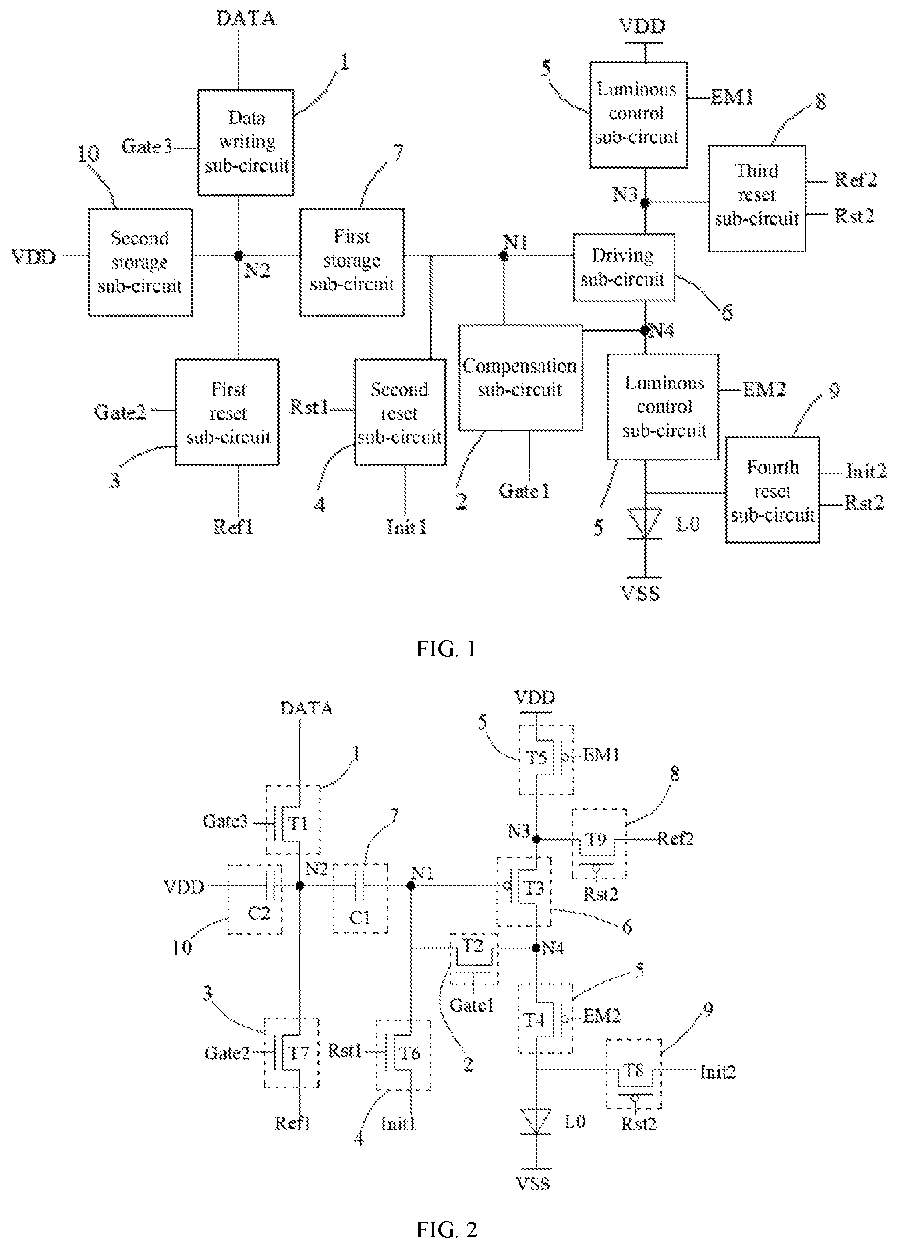
is a block diagram of a pixel circuit of an embodiment of the present disclosure.
is a circuit diagram of a pixel circuit of an embodiment of the present disclosure.
A , B and C are operating timing diagrams of the pixel circuit shown in .
is a schematic simulation diagram of a pixel circuit of an embodiment of the present disclosure.
is a schematic arrangement diagram of sub-pixels of an embodiment of the present disclosure.
Reference numerals: 1 , data writing sub-circuit; 2 , compensation sub-circuit; 3 , first reset sub-circuit; 4 , second reset sub-circuit; 5 , luminous control sub-circuit; 6 , driving sub-circuit; 7 , first storage sub-circuit; 8 , third reset sub-circuit; 9 , fourth reset sub-circuit; 10 , second storage sub-circuit; 11 , sub-pixel row; 12 , sub-pixel column; EM 1 , first luminous control signal end; EM 2 , second luminous control signal end; Rst 1 , first reset signal end; Rst 2 , second reset signal end; Gate 1 , first scan signal end; Gate 2 , second scan signal end; Gate 3 , third scan signal end; Init 1 , first initialization signal end; Init 2 , second initialization signal end; Ref 1 , first reference voltage end; Ref 2 , second reference voltage end; VDD, first power end; C 1 , first capacitor; C 2 , second capacitor; L 0 , sub-pixel; T 1 , data writing transistor; T 2 , compensation transistor; T 3 , driving transistor; T 4 second luminous control transistor; T 5 , first luminous control transistor; T 6 second reset transistor; T 7 , first reset transistor; T 8 , fourth reset transistor; T 9 , third reset transistor.
DETAILED DESCRIPTION
Description will now be made in detail to illustrative embodiments, examples of which are shown in the accompanying drawings. When the following description refers to the drawings, unless otherwise indicated, same reference numerals in different drawings indicate the same or similar elements. Embodiments described in the following illustrative embodiments do not represent all embodiments consistent with the present disclosure. In contrary, they are merely examples of apparatuses consistent with some aspects of the present disclosure as described in detail in the appended claims.
The terminologies used in the present disclosure are for the purpose of describing specific embodiments only and are not intended to limit the present disclosure. Unless otherwise defined, technical terms or scientific terms used in the present disclosure shall have their ordinary meanings as understood by those of ordinary skills in the field to which the present disclosure belongs. The “first”, “second” and similar words used in the specification and claims of the present disclosure do not indicate any order, quantity or importance, but are only used to distinguish different components. Similarly, similar words such as “a” or “an” do not mean quantity limitation, but mean that there is at least one. “Multiple” or “a plurality of” means two or more. Unless otherwise specified, similar words such as “front”, “rear” “lower” and/or “upper” are only for convenience of explanation, and are not limited to a position or a spatial orientation. Similar words such as “include” or “comprise” mean that the elements or objects appear before “include” or “comprise” cover the elements or objects listed after “include” or “comprise” and their equivalents, but do not exclude other elements or objects. When describing some embodiments, expressions of “connection” and “couple” and their derivations may be used. For example, when describing some embodiments, the term “connection” may be used to indicate that two or more components are in direct physical contact or electrical contact with each other. For another example, when describing some embodiments, the term “couple” may be used to indicate that two or more components are in direct physical contact or electrical contact. However, the term “connection” may also indicate that two or more components are not in direct contact with each other, but still cooperate or interact with each other. Singular forms “a”, “the” and “said” used in the specification of the present disclosure and the appended claims are also intended to include plural forms, unless the context clearly indicates other meaning. It should also be understood that the term “and/or” as used herein refers to and includes any or all possible combinations of one or more associated listed items.
The transistors used in the present disclosure can all be triodes, thin film transistors or field effect transistors or other components with same characteristics. In the embodiments of the present disclosure, in order to distinguish two electrodes of a transistor except for a control electrode, one of them is referred to as a first electrode and the other is referred to as a second electrode.
In practical operations, when the transistor is a triode, the control electrode can be a base, the first electrode can be a collector, and the second electrode can be an emitter; or, the control electrode can be a base, the first electrode can be an emitter, and the second electrode can be a collector.
In practical operations, when the transistor is a thin-film transistor or a field effect transistor, the control electrode can be a gate, the first electrode can be a drain and the second electrode can be a source; or, the control electrode can be a gate, the first electrode can be a source and the second electrode can be a drain.
An embodiment of the present disclosure provides a pixel circuit. The pixel circuit is applied to a display apparatus. As shown in , the display apparatus may include a plurality of sub-pixels L 0 and a plurality of pixel circuits, where the plurality of pixel circuits drive the plurality of sub-pixels L 0 to emit light in a one-to-one correspondence. The plurality of sub-pixels L 0 include first sub-pixels, second sub-pixels and third sub-pixels. The first sub-pixels, the second sub-pixels and the third sub-pixels have different luminous colors. For example, the first sub-pixels emit red light, the second sub-pixels emit green light, and the third sub-pixels emit blue light. The above-mentioned plurality of sub-pixels L 0 can be distributed in an array, and constitute a plurality of sub-pixel rows 11 and a plurality of sub-pixel columns 12 . A sub-pixel row 11 includes a plurality of sub-pixels L 0 distributed along a row direction, and a sub-pixel column 12 includes a plurality of sub-pixels L 0 distributed along a column direction. A first sub-pixel, a second sub-pixel and a third sub-pixel can form a pixel. The plurality of sub-pixels L 0 may form a plurality of pixels.
As shown in , the pixel circuit may include a first storage sub-circuit 7 , a data writing sub-circuit 1 , a driving sub-circuit 6 , a compensation sub-circuit 2 and a luminous control sub-circuit 5 .
The first storage sub-circuit 7 is connected between a first node N 1 and a second node N 2 . The data writing sub-circuit 1 is connected to the second node N 2 , and is configured to charge the second node N 2 . The driving sub-circuit 6 is connected to the first node N 1 , a third node N 3 and a fourth node N 4 , and is configured to control connection or disconnection between the third node N 3 and the fourth node N 4 under control of the first node N 1 . The compensation sub-circuit 2 is connected to a first scan signal end Gate 1 , the first node N 1 and the fourth node N 4 , and is configured to control connection or disconnection between the first node N 1 and the fourth node N 4 under control of the first scan signal end Gate 1 . The luminous control sub-circuit 5 is connected to a first power end VDD, a first luminous control signal end EM 1 , the third node N 3 , the fourth node N 4 , a second luminous control signal end EM 2 and a first electrode of a sub-pixel L 0 , and is configured to control connection or disconnection between the first power end VDD and the third node N 3 under control of the first luminous control signal end EM 1 , and is configured to control connection or disconnection between the fourth node N 4 and the first electrode of the sub-pixel L 0 under control of the second luminous control signal end EM 2 .
According to the pixel circuit of the embodiment of the present disclosure, during a driving process, a driving sub-circuit 6 is caused to control connection between a third node N 3 and a fourth node N 4 , a compensation sub-circuit 5 is caused to control connection between a first node N 1 and the fourth node N 4 , a luminous control sub-circuit 5 is caused to control connection between a first power end VDD and the third node N 3 , so that the first node N 1 can be charged through the first power end VDD, and a threshold voltage can be compensated to the driving sub-circuit 6 , so that a problem of poor display effect caused by different threshold voltages can be solved, thereby improving display effect; at the same time, the threshold voltage compensation of the present disclosure is not influenced by writing time of a data signal, and compensation effect can be improved by adding a compensation time.
Respective parts of the pixel circuit according to the embodiment of the present disclosure will be described in detail below.
As shown in and , the data writing sub-circuit 1 is connected to the second node N 2 , and is configured to charge the second node N 2 . Specifically, the data writing sub-circuit 1 can be connected to a data signal end DATA, a third scan signal end Gate 3 and the second node N 2 , and is configured to control connection or disconnection between the data signal end DATA and the second node N 2 under control of the third scan signal end Gate 3 . For example, the data writing sub-circuit 1 can include a data writing transistor T 1 . A control electrode of the data writing transistor T 1 is connected to the third scan signal end Gate 3 , a first electrode of the data writing transistor T 1 is connected to the data signal end DATA, and a second electrode of the data writing transistor T 1 is connected to the second node N 2 . The data writing transistor T 1 can be an oxide thin-film transistor, or certainly, can be a low-temperature polysilicon thin-film transistor.
As shown in and , the first storage sub-circuit 7 is connected between the first node N 1 and the second node N 2 . For example, the first storage sub-circuit 7 includes a first capacitor C 1 , a first electrode of the first capacitor C 1 is connected to the first node N 1 , and a second electrode of the first capacitor C 1 is connected to the second node N 2 .
As shown in and , the driving sub-circuit 6 is connected to the first node N 1 , the third node N 3 and the fourth node N 4 , and is configured to control connection or disconnection between the third node N 3 and the fourth node N 4 under control of the first node N 1 . For example, the driving sub-circuit 6 can include a driving transistor T 3 . A control electrode of the driving transistor T 3 is connected to the first node N 1 , a first electrode of the driving transistor T 3 is connected to the third node N 3 , and a second electrode of the driving transistor T 3 is connected to the fourth node N 4 . The driving transistor T 3 can be an oxide thin-film transistor, or certainly, can be a low-temperature polysilicon thin-film transistor.
As shown in and , the compensation sub-circuit 2 is connected to a first scan signal end Gate 1 , the first node N 1 and the fourth node N 4 , and is configured to control connection or disconnection between the first node N 1 and the fourth node N 4 under control of the first scan signal end Gate 1 . For example, the compensation sub-circuit 2 can include a compensation transistor T 2 . A control electrode of the compensation transistor T 2 is connected to the first scan signal end Gate 1 , a first electrode of the compensation transistor T 2 is connected to the fourth node N 4 , and a second electrode of the compensation transistor T 2 is connected to the first node N 1 . The compensation transistor T 2 can be an oxide thin-film transistor, or certainly, can be a low-temperature polysilicon thin-film transistor. A plurality of pixel circuits connected to the plurality of sub-pixels L 0 in a sub-pixel row 11 in a one-to-one correspondence can be connected to a same first scan signal end Gate 1 , that is, compensation sub-circuits 2 of the plurality of pixel circuits connected to the plurality of sub-pixels L 0 in the sub-pixel row 11 in a one-to-one correspondence can be connected to the same first scan signal end Gate 1 . The plurality of sub-pixel rows 11 constitute one or more pixel groups. One pixel group can include a plurality of sub-pixel rows 11 , for example, two sub-pixel rows 11 , three sub-pixel rows 11 , or fourth sub-pixel rows 11 , etc. A number of sub-pixel rows 11 in different pixel groups is the same. A plurality of pixel circuits correspondingly connected to sub-pixels L 0 in a pixel group are connected to a same first scan signal end Gate 1 .
As shown in and , the luminous control sub-circuit 5 is connected to a first power end VDD, a first luminous control signal end EM 1 , the third node N 3 , the fourth node N 4 , a second luminous control signal end EM 2 and a first electrode of a sub-pixel L 0 , and is configured to control connection or disconnection between the first power end VDD and the third node N 3 under control of the first luminous control signal end EM 1 , and is configured to control connection or disconnection between the fourth node N 4 and the first electrode of the sub-pixel L 0 under control of the second luminous control signal end EM 2 . For example, the luminous control sub-circuit 5 can include a first luminous control transistor T 5 and a second luminous control transistor T 4 . A control electrode of the first luminous control transistor T 5 is connected to the first luminous control signal end EM 1 , a first electrode of the first luminous control transistor T 5 is connected to the first power end VDD, and a second electrode of the first luminous control transistor T 5 is connected to the third node N 3 . The first luminous control transistor T 5 can be an oxide thin-film transistor, or certainly, can be a low-temperature polysilicon thin-film transistor. A control electrode of the second luminous control transistor T 4 is connected to the second luminous control signal end EM 2 , a first electrode of the second luminous control transistor T 4 is connected to the fourth node N 4 , and a second electrode of the second luminous control transistor T 4 is connected to the first electrode of the sub-pixel L 0 . A second electrode of the sub-pixel L 0 can be connected to a second power end VSS. The second luminous control transistor T 4 can be an oxide thin-film transistor, or certainly, can be a low-temperature polysilicon thin-film transistor. In addition, a plurality of pixel circuits correspondingly connected to sub-pixels L 0 in a pixel group are connected to a same first luminous control signal end EM 1 . A plurality of pixel circuits correspondingly connected to sub-pixels L 0 in a pixel group are connected to a same second luminous control signal end EM 2 .
As shown in and , the pixel circuit of the present disclosure may further include a first reset sub-circuit 3 . The first reset sub-circuit 3 can be connected to a second scan signal end Gate 2 , a first reference voltage end Ref 1 and the second node N 2 , and can be configured to control connection or disconnection between the first reference voltage end Ref 1 and the second node N 2 under control of the second scan signal end Gate 2 . For example, the first reset sub-circuit 3 can include a first reset transistor T 7 . A control electrode of the first reset transistor T 7 is connected to the second scan signal end Gate 2 , a first electrode of the first reset transistor T 7 is connected to the first reference voltage end Ref 1 , and a second electrode of the first reset transistor T 7 is connected to the second node N 2 . The first reset transistor T 7 can be an oxide thin-film transistor, or certainly, can be a low-temperature polysilicon thin-film transistor. As shown in A , within a frame, a time period that the first reset sub-circuit 3 controls the first reference voltage end Ref 1 to connect to the second node N 2 (i.e., a time period that the second scan signal end Gate 2 being high as shown in the figure) is before that the data writing sub-circuit 1 charges the second node N 2 , which can ensure that an electric potential of the second node N 2 within a data writing stage t 3 within a current frame is not influenced by a data signal written into the second node N 2 by the data signal end DATA in a previous frame. In addition, within a frame, a start time that the first reset sub-circuit 3 controls the first reference voltage end Ref 1 to connect to the second node N 2 (i.e., a time that the second scan signal end Gate 2 jumps from low to high as shown in the figure) is before a start time that the compensation sub-circuit 2 controls the first node N 1 to connect to the fourth node N 4 (i.e., a time that the first scan signal end Gate 1 jumps from low to high as shown in the figure). In such way, it is ensured that an electric potential of the second node N 2 within a compensation stage t 2 within a current frame is not influenced by a data signal written into the second node N 2 by the data signal end DATA in a previous frame. In addition, a plurality of pixel circuits correspondingly connected to sub-pixels L 0 in a pixel group are connected to a same second scan signal end Gate 2 .
As shown in and , the pixel circuit of the present disclosure may further include a second reset sub-circuit 4 . The second reset sub-circuit 4 can be connected to a first reset signal end Rst 1 , a first initialization signal end Init 1 and the first node N 1 , and is configured to control connection or disconnection between the first initialization signal end Init 1 and the first node N 1 under control of the first reset signal end Rst 1 . For example, the second reset sub-circuit 4 can include a second reset transistor T 6 . A control electrode of the second reset transistor T 6 is connected to the first reset signal end Rst 1 , a first electrode of the second reset transistor T 6 is connected to the first initialization signal end Init 1 , and a second electrode of the second reset transistor T 6 is connected to the first node N 1 . The second reset transistor T 6 can be an oxide thin-film transistor, or certainly, can be a low-temperature polysilicon thin-film transistor. In addition, a plurality of pixel circuits correspondingly connected to sub-pixels L 0 in a pixel group are connected to a same first reset signal end Rst 1 .
As shown in and , the pixel circuit of the present disclosure may further include a third reset sub-circuit 8 . The third reset sub-circuit 8 can be connected to a second reset signal end Rst 2 , a second reference voltage end Ref 2 and the third node N 3 , and can be configured to control connection or disconnection between the second reference voltage end Ref 2 and the third node N 3 under control of the second reset signal end Rst 2 . For example, the third reset sub-circuit 8 can include a third reset transistor T 9 . A control electrode of the third reset transistor T 9 is connected to the second reset signal end Rst 2 , a first electrode of the third reset transistor T 9 is connected to the second reference voltage end Ref 2 , and a second electrode of the third reset transistor T 9 is connected to the third node N 3 . The third reset transistor T 9 can be an oxide thin-film transistor, or certainly, can be a low-temperature polysilicon thin-film transistor. In addition, a plurality of pixel circuits correspondingly connected to sub-pixels L 0 in a pixel group are connected to a same second reset signal end Rst 2 .
As shown in and , the pixel circuit of the present disclosure may further include a fourth reset sub-circuit 9 . The fourth reset sub-circuit 9 can be connected to the second reset signal end Rst 2 , a second initialization signal end Init 2 and the first electrode of the sub-pixel L 0 , and is configured to control connection or disconnection between the second initialization signal end Init 2 and the first electrode of the sub-pixel L 0 under control of the second reset signal end Rst 2 . For example, the fourth reset sub-circuit 9 can include a fourth reset transistor T 8 . A control electrode of the fourth reset transistor T 8 is connected to the second reset signal end Rst 2 , a first electrode of the fourth reset transistor T 8 is connected to the second initialization signal end Init 2 , and a second electrode of the fourth reset transistor T 8 is connected to the first electrode of the sub-pixel L 0 . The fourth reset transistor T 8 can be an oxide thin-film transistor, or certainly, can be a low-temperature polysilicon thin-film transistor.
As shown in and , the pixel circuit of the present disclosure may further include a second storage sub-circuit 10 . The second storage sub-circuit 10 is connected between the first power end VDD and the second node N 2 . For example, the second storage sub-circuit 10 can include a second capacitor C 2 , where a first electrode of the second capacitor C 2 is connected to the second node N 2 , and a second electrode of the second capacitor C 2 is connected to the first power end VDD.
As shown in , and A , within a frame, a driving process of the pixel circuit includes a compensation stage t 2 , a data writing stage t 3 and a display stage t 4 , where the compensation stage t 2 is before the data writing stage t 3 , and the display stage t 4 is after the data writing stage t 3 . In the compensation stage t 2 , the luminous control sub-circuit 5 controls the first power end VDD to connect to the third node N 3 , the compensation sub-circuit 2 controls the first node N 1 to connect to the fourth node N 4 , that is, the first power end VDD is connected to the third node N 3 through the first luminous control transistor T 5 , the first node N 1 is connected to the fourth node N 4 through the compensation transistor T 2 . In the data writing stage t 3 , the data writing sub-circuit 1 charges the second node N 2 , that is, the data signal end DATA is connected to the second node N 2 through the data writing transistor T 1 . In the display stage t 4 , the luminous control sub-circuit 5 controls the first power end VDD to connect to the third node N 3 , the luminous control sub-circuit 5 further controls the fourth node N 4 to connect to the first electrode of the sub-pixel L 0 , that is, the first power end VDD is connected to the third node N 3 through the first luminous control transistor T 5 , the fourth node N 4 is connected to the first electrode of the sub-pixel L 0 through the second luminous control transistor T 4 . Within a frame, for a plurality of sub-pixel rows 11 in a pixel group, a time interval between a start time that the data writing sub-circuit 1 in the pixel circuit connected to a first one of the sub-pixel rows 11 charges the second node N 2 and an end time of the compensation stage t 2 is greater than a charging duration that the data writing sub-circuit 1 charges the second node N 2 . Within a frame, for a plurality of sub-pixels rows 11 in a pixel group, a time interval between an end time that the data writing sub-circuit 1 in the pixel circuit connected to a last one of the sub-pixel rows 11 charges the second node N 2 and a start time of the display stage t 4 is greater than a charging duration that the data writing sub-circuit 1 charges the second node N 2 .
In addition, as shown in A , within a frame, a driving process of the pixel circuit may further include an initialization stage t 1 , where the initialization stage t 1 is before the compensation stage t 2 . In the initialization stage t 1 , the first reset sub-circuit 3 controls the first reference voltage end Ref 1 to connect to the second node N 2 , the second reset sub-circuit 4 controls the first initialization signal end Init 1 to connect to the first node N 1 , the third reset sub-circuit 8 controls the second reference voltage end Ref 2 to connect to the third node N 3 , the fourth reset sub-circuit 9 controls the second initialization signal end Init 2 to connect to the first electrode of the sub-pixel L 0 , that is, the first reference voltage end Ref 1 is connected to the second node N 2 through the first reset transistor T 7 , the first initialization signal end Init 1 is connected to the first node N 1 through the second reset transistor T 6 , the second reference voltage end Ref 2 is connected to the third node N 3 through the third reset transistor T 9 , the second initialization signal end Init 2 is connected to the first electrode of the sub-pixel L 0 through the fourth reset transistor T 8 .
The plurality of sub-pixel rows 11 of the display apparatus may include n-th to m-th sub-pixel rows 11 , where n is greater than or equal to 1, m is greater than n, m is less than or equal to a number of sub-pixel rows 11 in the display apparatus. The n-th to m-th sub-pixel rows 11 can constitute a pixel group as mentioned above. The n-th to m-th sub-pixel rows 11 can include an f-th sub-pixel row 11 and a (f+1)-th sub-pixel row 11 , where f is greater than or equal to n, and (f+1) is less than or equal to m. A start time that the data writing sub-circuit 1 in the pixel circuit connected to the f-th sub-pixel row 11 charges the second node N 2 is before a start time that the data writing sub-circuit 1 in the pixel circuit connected to the (f+1)-th sub-pixel row 11 charges the second node N 2 .
It is taken as an example that a plurality of pixel circuits correspondingly connected to a plurality of sub-pixels L 0 in the n-th to m-th sub-pixel rows 11 are connected to a same first scan signal end Gate 1 , the compensation stage t 2 of the plurality of pixel circuits correspondingly connected to the plurality of sub-pixels L 0 in the n-th to m-th sub-pixel rows 11 is after a start time that the luminous control sub-circuit 5 in the pixel circuit connected to the m-th sub-pixel row 11 controls the first power end VDD to connect to the third node N 3 , and is before a start time that the data writing sub-circuit 1 in the pixel circuit connected to the n-th sub-pixel row 11 charges the second node N 2 .
For example, in C , it is taken as an example that the n-th to m-th sub-pixel rows 11 constitute a pixel group, a plurality of pixel circuits correspondingly connected to a plurality of sub-pixels L 0 in the n-th to m-th sub-pixel rows 11 are connected to a same first scan signal end Gate 1 (n-th to m-th), the plurality of pixel circuits correspondingly connected to the plurality of sub-pixels L 0 in the n-th to m-th sub-pixel rows 11 are connected to a same second scan signal end Gate 2 (n-th to m-th), the plurality of pixel circuits correspondingly connected to the plurality of sub-pixels L 0 in the n-th to m-th sub-pixel rows 11 are connected to a same first reset signal end Rst 1 (n-th to m-th), the plurality of pixel circuits correspondingly connected to the plurality of sub-pixels L 0 in the n-th to m-th sub-pixel rows 11 are connected to a same second reset signal end Rst 2 (n-th to m-th), the plurality of pixel circuits correspondingly connected to the plurality of sub-pixels L 0 in the n-th to m-th sub-pixel rows 11 are connected to a same first luminous control signal end EM 1 (n-th to m-th), the plurality of pixel circuits correspondingly connected to the plurality of sub-pixels L 0 in the n-th to m-th sub-pixel rows 11 are connected to a same second luminous control signal end EM 2 (n-th to m-th); in such arrangement, wiring can be reduced, layout area of a gate driving circuit can be saved, which is equivalent to that a plurality of sub-pixel rows 11 share a same level of shift register, which is beneficial to realization of a narrow frame; at the same time, a frequency of a clock signal input to the gate driving circuit can be reduced, and a demand for a driving chip can be reduced. The driving chip is configured to provide a clock signal to the gate driving circuit. A pixel circuit connected to the n-th sub-pixel row 11 is connected to a third scan signal end Gate 3 ( n ), a pixel circuit connected to the (n+1)-th sub-pixel row 11 is connected to a third scan signal end Gate 3 ( n+ 1), a pixel circuit connected to the m-th sub-pixel row 11 is connected to a third scan signal end Gate 3 ( m ); the compensation stage t 2 of the plurality of pixel circuits correspondingly connected to the plurality of sub-pixels L 0 in the n-th to m-th sub-pixel rows 11 is after a start time that the luminous control sub-circuit 5 in the pixel circuit connected to the m-th sub-pixel row 11 controls the first power end VDD to connect to the third node N 3 , and is before a start time that the data writing sub-circuit 1 in the pixel circuit connected to the n-th sub-pixel row 11 charges the second node N 2 ; the display stage t 4 of the plurality of pixel circuits correspondingly connected to the plurality of sub-pixels L 0 in the n-th to m-th sub-pixel rows 11 is after an end time that the data writing sub-circuit 1 in the pixel circuit connected to the m-th sub-pixel row 11 charges the second node N 2 , that is, the n-th to m-th sub-pixel rows 11 emit light uniformly.
In addition, in C , a time interval ΔT 1 between a start time that the data writing sub-circuit 1 in the pixel circuit connected to the n-th sub-pixel row 11 charges the second node N 2 and an end time of the compensation stage t 2 is greater than a charging duration ΔT that the data writing sub-circuit 1 charges the second node N 2 , where the charging duration ΔT is a duration that the third scan signal end Gate 3 being at an effective electric level, that is, within ΔT, the third scan signal end Gate 3 controls the data writing transistor T 1 to turn on; within a frame, a time interval ΔT 2 between an end time that the data writing sub-circuit 1 in the pixel circuit connected to the m-th sub-pixel row 11 charges the second node N 2 and a start time of the display stage t 4 is greater than a charging duration ΔT that the data writing sub-circuit 1 charges the second node N 2 ; the above ΔT 1 and ΔT 2 may be equal, or certainly, not equal; in such arrangement, the time interval ΔT 1 and the time interval ΔT 12 are increased, so that a ratio of a phase difference between any two third scan signal ends Gate 3 to a total duration of the data writing stage t 3 is reduced, and the display is more uniform.
In the following, an operating process of the pixel circuit in will be described in detail with reference to an operating timing diagram of the pixel circuit shown in A . The data writing transistor T 1 , the first reset transistor T 7 , the second reset transistor T 6 and the compensation transistor T 2 are N-type transistors, and a turn-on electric level thereof is a high electric level; the first luminous control transistor T 5 , the third reset transistor T 9 , the driving transistor T 3 , the second luminous control transistor T 4 and the fourth reset transistor T 8 are P-type transistors, and a turn-on electric level thereof is a low electric level.
As shown in and A , in the initialization stage t 1 , the first luminous control signal end EM 1 , the second luminous control signal end EM 2 , the first reset signal end Rst 1 and the second scan signal end Gate 2 are at high electric levels, the second reset signal end Rst 2 , the first scan signal end Gate 1 and the third scan signal end Gate 3 are at low electric levels, the first reset transistor T 7 , the second reset transistor T 6 , the fourth reset transistor T 8 and the third reset transistor T 9 are turned on; the first reference voltage end Ref 1 and the second node N 2 are connected, the second node N 2 is reset; the first initialization signal end Init 1 is connected to the first N 1 , the first node N 1 is reset; the second initialization signal end Init 2 is connected to the first electrode of the sub-pixel L 0 , the first electrode of the sub-pixel L 0 is reset; the second reference voltage end Ref 2 is connected to the third node N 3 , and the third node N 3 is reset. Since both the first node N 1 and the second node N 2 are reset to an initial voltage, the first capacitor C 1 and the second capacitor C 2 are also initialized.
As shown in and A , in the compensation stage t 2 , the first luminous control signal end EM 1 and the first reset signal end Rst 1 jump to a low electric level, the first scan signal end Gate 1 and the second reset signal end Rst 2 jump to a high electric level, the second luminous control signal end EM 2 and the second scan signal end Gate 2 remain in a high electric level, the third scan signal end Gate 3 remains in a low electric level; the second reset transistor T 6 , the fourth reset transistor T 8 and the third reset transistor T 9 are turned off, the first reset transistor T 7 remains turned on and is configured to stabilize a voltage of the second node N 2 (the voltage is written as Vref 1 by the first reference voltage end Ref 1 ); the first luminous control transistor T 5 is turned on, the driving transistor T 3 is turned on (in the initialization stage t 1 , the driving transistor T 3 is turned on by setting an electric potential of the first initialization signal end Init 1 ), the compensation transistor T 2 is turned on, the first power end VDD is connected to the first node N 1 , and when a voltage of the first node N 1 is written as [VDD+Vth(T 3 )], the driving transistor T 3 is turned off.
As shown in and A , in the data writing stage t 3 , the first scan signal end Gate 1 and the second scan signal end Gate 2 jump to a low electric level in turn, the third scan signal end Gate 3 jump to a high electric level, the data writing transistor T 1 is turned on, the data signal end DATA is connected to the second node N 2 , a voltage of the second node N 2 is written as Vdata by the data signal end DATA, and under coupling effect of the first capacitor, a voltage of the first node N 1 changes by (Vdata−Vref 1 )*a, where a is related to a ratio between the first capacitor C 1 and the second capacitor C 2 , and at this time, a voltage of the first node N 1 is [VDD+Vth(T 3 )+(Vdata−Vref 1 )*a]. It can be seen that the compensation stage t 2 of the present disclosure is carried out separately from the data writing stage t 3 , and the compensation stage t 2 is not influenced by a writing time of the data signal end DATA, and compensation effect can be improved by increasing a duration of the compensation stage t 2 .
As shown in and A , in the display stage t 4 , the third scan signal end Gate 3 and the second luminous control signal end EM 2 jump to a low electric level, the driving transistor T 3 , the second luminous control transistor T 4 and the first luminous control transistor T 5 are turn on, and the sub-pixel L 0 emits light. A luminous current formula is: I=½*μ*Cox*W/L*(Vgs−Vth){circumflex over ( )}2=½*μ*Cox*W/L*[(Vdata−Vref 1 )*a]{circumflex over ( )}2, where p represents electron mobility, Cox represents gate oxide capacitance, Vgs represents a voltage difference between a control electrode and a first electrode of the driving transistor T 3 , W/L represents a ratio of width to length of a channel area of the driving transistor T 3 . It can be seen that the luminous formula does not contain a factor of Vth(T 3 ), which means that the pixel circuit can compensate a threshold voltage of the driving transistor T 3 to bring better display uniformity. is a schematic simulation diagram of a pixel circuit.
Compared to A , a difference that the pixel circuit of operates according to the timing diagram of B is that: in the display stage t 4 , a pulse width modulation (PWM) is adopted for light adjustment, and specifically, an emitting duration of the sub-pixel L 0 is controlled through an electric potential of the first luminous control signal end EM 1 , and a luminance of the sub-pixel L 0 can be further controlled.
Compared to A , a difference that the pixel circuit of operates according to the timing diagram of B is that: in the data writing stage t 3 , a plurality of third scan signal ends Gate 3 [Gate 3 ( n ), Gate 3 ( n+ 1), . . . , Gate 3 ( m )] jump to a high electric level in turn, and second nodes N 2 of pixel circuits connected to different sub-pixel rows 11 are written as Vdata in turn.
An embodiment of the present disclosure further provides a driving method for a pixel circuit, configured to drive the pixel circuit in the above embodiments. The driving method for the pixel circuit includes: causing a driving sub-circuit 6 to control connection or disconnection between a third node N 3 and a fourth node N 4 under control of a first node N 1 ; causing a compensation sub-circuit 2 to control connection or disconnection between the first node N 1 and the fourth node N 4 under control of a first scan signal end Gate 1 ; causing a luminous control sub-circuit 5 to control connection or disconnection between a first power end VDD and the third node N 3 under control of a first luminous control signal end EM 1 , and further causing the luminous control sub-circuit 5 to control connection or disconnection between the fourth node N 4 and a first electrode of a sub-pixel L 0 under control of a second luminous control signal EM 2 . Since the pixel circuit driven by the driving method of the embodiment of the present disclosure is same as the pixel circuit in the above-mentioned embodiments, it has same beneficial effects, which will not be repeated here.
An embodiment of the present disclosure further provides a display apparatus. The display apparatus may include the pixel circuit or the sub-pixel connected to the pixel circuit according to any one of the above embodiments. The display apparatus can be a portable phone, a smart phone, a video phone, a smart tablet, a smart watch, a tablet personal computer, a navigation system for vehicles, a television, a computer monitor, a notebook computer, a head-mounted display and any other products or components with display functions. Since the pixel circuit in the display apparatus of the embodiment of the present disclosure is same as the pixel circuit in the above-mentioned embodiments, it has same beneficial effects, which will not be repeated here.
The above are only preferred embodiments of the present disclosure, and they do not limit the present disclosure in any form. Although the present disclosure has been disclosed in the preferred embodiments, they are not used to limit the present disclosure. Any person familiar with this profession can make some changes or modify it into an equivalent embodiment by using the technical content disclosed above without departing from the scope of the technical solution of the present disclosure. So long as the content does not depart from the technical solution of the present disclosure, any simple modifications, equivalent changes or modifications made to the above embodiments according to the technical essence of the present disclosure belong to the scope of the technical solution of the present disclosure.
Figures (4)
Citations
This patent cites (20)
- US2018/0341357
- US2018/0342193
- US2018/0342200
- US2018/0342203
- US2018/0342213
- US2018/0342570
- US2021/0201773
- US2021/0375192
- US2021/0376041
- US2023/0024280
- US2023/0042603
- US111696473
- US111696486
- US112259041
- US112509518
- US113744676
- US113838415
- US115101011
- US115512656
- US20200055580