Abstract
A display includes a first light emitting device. The first light emitting device includes a first switch and a second switch. The first switch is configured to adjust a first node according to a first clock signal. The second switch is configured to generate a first light emitting signal according to a first voltage signal. A control end of the second switch is coupled to the first node. The first clock signal switches between a first voltage level and a second voltage level. The first voltage signal has a third voltage level. The third voltage level is more than one of the first voltage level and the second voltage level and is less than the other one of the first voltage level and the second voltage level.
Claims (16)
1. A display, comprising: a first light emitting device, comprising: a first switch configured to adjust a first node according to a first clock signal; and a second switch configured to generate a first light emitting signal according to a first voltage signal, and a control end of the second switch is coupled to the first node, wherein the first clock signal switches between a first voltage level and a second voltage level, the first voltage signal has a third voltage level, and the third voltage level is more than one of the first voltage level and the second voltage level and is less than the other one of the first voltage level and the second voltage level, wherein an absolute value of a voltage difference between the second voltage level and the third voltage level is greater than or equal to a threshold voltage of the first switch.
9. A display device, comprising: a first switch configured to adjust a first node according to a first clock signal; a capacitor; and a second switch configured to generate a first light emitting signal according to a first voltage signal, and a control end of the second switch is coupled to the first node, wherein a first end of the capacitor is configured to receive a second clock signal complementary to the first clock signal, a second end of the capacitor is coupled to the first node, the first clock signal switches between a first voltage level and a second voltage level, the first voltage signal has a third voltage level, and the third voltage level is more than one of the first voltage level and the second voltage level and is less than the other one of the first voltage level and the second voltage level, wherein an absolute value of a voltage difference between the second voltage level and the third voltage level is greater than or equal to a threshold voltage of the first switch.
Show 14 dependent claims
2. The display of claim 1 , further comprising: a third switch coupled to the first switch, a control end of the third switch is configured to receive a first control signal; and a fourth switch coupled to the first switch, a control end of the fourth switch is configured to receive a second control signal, wherein the first control signal and the second control signal are complementary to each other.
3. The display of claim 2 , wherein when one of the first control signal and the second control signal has the first voltage level, the other one of the first control signal and the second control signal has the second voltage level.
4. The display of claim 1 , further comprising: a third switch configured to generate a first driving signal according to a second voltage signal, a control end of the third switch is coupled to the first node, wherein the second voltage signal has a fourth voltage level, and the fourth voltage level is larger than one of the second voltage level and the third voltage level and is less than the other one of the second voltage level and the third voltage level.
5. The display of claim 4 , wherein an absolute value of a voltage difference between the fourth voltage level and the third voltage level is greater than or equal to a threshold voltage of the second switch.
6. The display of claim 5 , wherein an absolute value of a voltage difference between the fourth voltage level and the second voltage level is greater than or equal to a threshold voltage of the first switch.
7. The display of claim 4 , further comprising: a fourth switch coupled to the first switch, a control end of the fourth switch is configured to receive a first control signal; and a fifth switch coupled to the first switch, a control end of the fifth switch is configured to receive a second control signal, wherein the first control signal and the second control signal are complementary to each other.
8. The display of claim 7 , wherein when one of the first control signal and the second control signal has the first voltage level, the other one of the first control signal and the second control signal has the second voltage level.
10. The display device of claim 9 , further comprising: a third switch coupled to the first switch, a control end of the third switch is configured to receive a first control signal; and a fourth switch coupled to the first switch, a control end of the fourth switch is configured to receive a second control signal, wherein the first control signal and the second control signal are complementary to each other.
11. The display device of claim 10 , wherein when one of the first control signal and the second control signal has the first voltage level, the other one of the first control signal and the second control signal has the second voltage level.
12. The display device of claim 9 , further comprising: a third switch configured to generate a first driving signal according to a second voltage signal, a control end of the third switch is coupled to the first node, wherein the second voltage signal has a fourth voltage level, and the fourth voltage level is larger than one of the second voltage level and the third voltage level and is less than the other one of the second voltage level and the third voltage level.
13. The display device of claim 12 , wherein an absolute value of a voltage difference between the fourth voltage level and the third voltage level is greater than or equal to a threshold voltage of the second switch.
14. The display device of claim 13 , wherein an absolute value of a voltage difference between the fourth voltage level and the second voltage level is greater than or equal to a threshold voltage of the first switch.
15. The display device of claim 12 , further comprising: a fourth switch coupled to the first switch, a control end of the fourth switch is configured to receive a first control signal; and a fifth switch coupled to the first switch, a control end of the fifth switch is configured to receive a second control signal, wherein the first control signal and the second control signal are complementary to each other.
16. The display device of claim 15 , wherein when one of the first control signal and the second control signal has the first voltage level, the other one of the first control signal and the second control signal has the second voltage level.
Full Description
Show full text →
CROSS-REFERENCE TO RELATED APPLICATION
This application claims priority to Taiwan Application Serial Number 112124798, filed Jul. 3, 2023, which is herein incorporated by reference in its entirety.
BACKGROUND
Technical Field
The present disclosure relates to a display technology. More particularly, the present disclosure relates to a display.
Description of Related Art
In order to improve the problem of uneven brightness (mura) of the display, the design of the picture compensation (demura) is added to the light-emitting circuit. However, the design of a single driving signal causes the transistor in the light-emitting circuit to operate in the saturation region, such that the output waveform of the light-emitting circuit is easily affected by the critical voltage of the transistor, and the problem of uneven brightness reappears with the advance of the operation time. Thus, techniques associated with the development for overcoming the problems described above are important issues in the field.
SUMMARY
The present disclosure provides a display. The display includes a first light emitting device. The first light emitting device includes a first switch and a second switch. The first switch is configured to adjust a first node according to a first clock signal. The second switch is configured to generate a first light emitting signal according to a first voltage signal. A control end of the second switch is coupled to the first node. The first clock signal switches between a first voltage level and a second voltage level. The first voltage signal has a third voltage level. The third voltage level is more than one of the first voltage level and the second voltage level and is less than the other one of the first voltage level and the second voltage level.
The present disclosure provides a display device. The display device includes a first switch, a capacitor, and a second switch. The first switch is configured to adjust a first node according to a first clock signal. The second switch is configured to generate a first light emitting signal according to a first voltage signal. A control end of the second switch is coupled to the first node. A first end of the capacitor is configured to receive a second clock signal complementary to the first clock signal. A second end of the capacitor is coupled to the first node. The first clock signal switches between a first voltage level and a second voltage level. The first voltage signal has a third voltage level. The third voltage level is more than one of the first voltage level and the second voltage level and is less than the other one of the first voltage level and the second voltage level.
It is to be understood that both the foregoing general description and the following detailed description are by examples, and are intended to provide further explanation of the disclosure as claimed.
BRIEF DESCRIPTION OF THE DRAWINGS
Aspects of the present disclosure are best understood from the following detailed description when read with the accompanying figures. It is noted that, in accordance with the standard practice in the industry, various features are not drawn to scale. In fact, the dimensions of the various features may be arbitrarily increased or reduced for clarity of discussion.
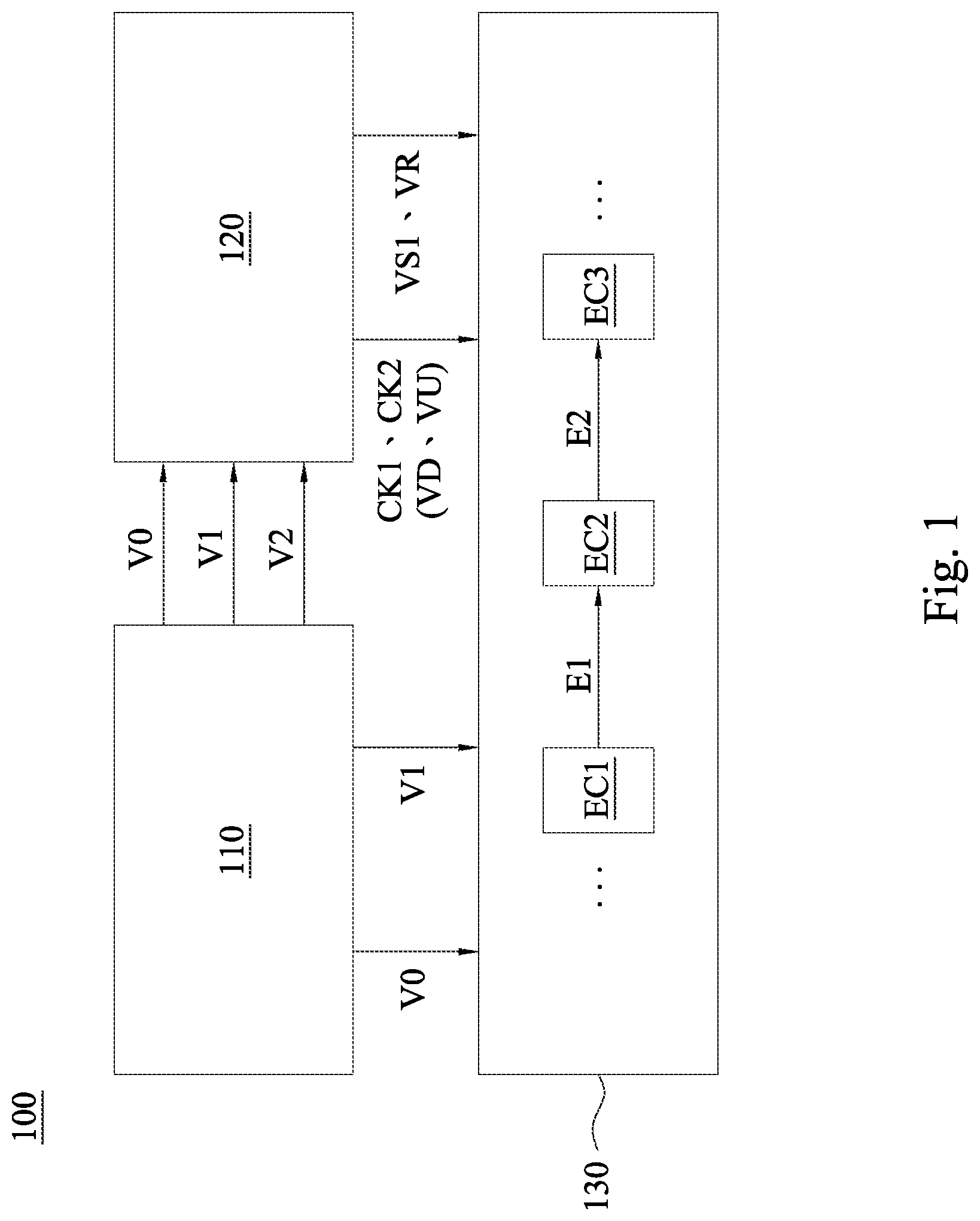
is a schematic diagram of a display illustrated according to some embodiments of present disclosure.
is a schematic diagram of a light emitting circuit corresponding to the light emitting circuit shown in illustrated according to some embodiments of present disclosure.
is a timing diagram of operations of a light emitting circuit illustrated according to some embodiments of present disclosure.
is a schematic diagram of a light emitting circuit corresponding to the light emitting circuit shown in illustrated according to some embodiments of present disclosure.
is a schematic diagram of a light emitting device corresponding to the light emitting device shown in illustrated according to some embodiments of present disclosure.
is a schematic diagram of a display illustrated according to some embodiments of present disclosure.
is a schematic diagram of a light emitting circuit corresponding to the light emitting circuits shown in illustrated according to some embodiments of present disclosure.
is a timing diagram of operations of a light emitting circuit illustrated according to some embodiments of present disclosure.
DETAILED DESCRIPTION
The following disclosure provides many different embodiments, or examples, for implementing different features of the provided subject matter. Specific examples of components and arrangements are described below to simplify the present disclosure. These are, of course, merely examples and are not intended to be limiting. For example, the formation of a first feature over or on a second feature in the description that follows may include embodiments in which the first and second features are formed in direct contact, and may also include embodiments in which additional features may be formed between the first and second features, such that the first and second features may not be in direct contact. In addition, the present disclosure may repeat reference numerals and/or letters in the various examples. This repetition is for the purpose of simplicity and clarity and does not in itself dictate a relationship between the various embodiments and/or configurations discussed.
Further, spatially relative terms, such as “beneath,” “below,” “lower,” “above,” “upper”, “left,” “right” and the like, may be used herein for ease of description to describe one element or feature's relationship to another element(s) or feature(s) as illustrated in the figures. The spatially relative terms are intended to encompass different orientations of the device in use or operation in addition to the orientation depicted in the figures. The apparatus may be otherwise oriented (rotated 90 degrees or at other orientations) and the spatially relative descriptors used herein may likewise be interpreted accordingly.
The terms applied throughout the following descriptions and claims generally have their ordinary meanings clearly established in the art or in the specific context where each term is used. Those of ordinary skill in the art will appreciate that a component or process may be referred to by different names. Numerous different embodiments detailed in this specification are illustrative only, and in no way limits the scope and spirit of the disclosure or of any exemplified term.
It is worth noting that the terms such as “first” and “second” used herein to describe various elements or processes aim to distinguish one element or process from another. However, the elements, processes and the sequences thereof should not be limited by these terms. For example, a first element could be termed as a second element, and a second element could be similarly termed as a first element without departing from the scope of the present disclosure.
In the following discussion and in the claims, the terms “comprising,” “including,” “containing,” “having,” “involving,” and the like are to be understood to be open-ended, that is, to be construed as including but not limited to. As used herein, instead of being mutually exclusive, the term “and/or” includes any of the associated listed items and all combinations of one or more of the associated listed items.
As used herein, “around”, “about” or “approximately” shall generally mean within 20 percent, preferably within 10 percent, and more preferably within 5 percent of a given value or range. Numerical quantities given herein are approximate, meaning that the term “around”, “about” or “approximately” can be inferred if not expressly stated.
Reference will now be made in detail to the present embodiments of the disclosure, examples of which are illustrated in the accompanying drawings. Wherever possible, the same reference numbers are used in the drawings and the description to refer to the same or like parts.
is a schematic diagram of a display 100 illustrated according to some embodiments of present disclosure. As shown in , the display 100 includes a power device 110 , a level shifting device 120 and a light emitting device 130 . In some embodiments, the power device 110 is configured to provide voltage signals V 0 -V 2 to the level shifting device 120 and provide voltage signals V 0 -V 1 to the light emitting device 130 . The level shifting device 120 is configured to provide clock signals CK 1 and CK 2 , control signals VS 1 and VR to the light emitting device 130 .
As shown in , the light emitting device 130 includes light emitting circuits EC 1 -EC 3 . In some embodiments, the light emitting circuit EC 1 is configured to output a light emitting signal E 1 to the light emitting circuit EC 2 , and the light emitting circuit EC 2 is configured to output a light emitting signal E 2 to the light emitting circuit EC 3 . In various embodiments, the light emitting device 130 may include various numbers of light emitting circuits. In some embodiments, the level shifting device 120 is further configured to provide control signals VD and VU to the light emitting device 130 , and the light emitting circuits EC 1 and EC 2 in the light emitting device 130 is further configured to generate the light emitting signals E 1 and E 2 according to the control signals VD and VU.
is a schematic diagram of a light emitting circuit 200 corresponding to the light emitting circuits EC 1 -EC 3 shown in illustrated according to some embodiments of present disclosure. As shown in , the light emitting circuit 200 includes an enabling unit 210 , a driving unit 220 and a discharging unit 230 . In some embodiments, the enabling unit 210 is configured to generate a node signal Q 1 according to a clock signal CK 1 and one of the control signal VS 1 and a light emitting signal EM 1 . The driving unit 220 is configured to generate a light emitting signal EM 2 according to the node signal Q 1 and the voltage signal V 1 . The discharging unit 230 is configured to discharge the driving unit 220 according to the node signal Q 1 , the voltage signals V 0 , V 1 , the clock signal CK 1 and one of the control signal VS 1 and the light emitting signal EM 1 . In some embodiments, the pixel circuit (not shown in the figure) in the display 100 as shown in is configured to emit light according to the light emitting signals EM 1 and EM 2 .
As shown in , the enabling unit 210 includes a switch T 21 . The driving unit 220 includes a switch T 22 and a capacitor C 22 . The discharging unit 230 includes switches T 23 -T 28 and a capacitor C 21 . In some embodiments, the switches T 21 -T 28 can be implemented by various transistors, such as by p-type metal oxide semiconductor (PMOS) transistors.
As shown in , each of a first end of the switch T 21 and a control end of the switch T 27 is configured to receive the control signal VS 1 or the light emitting signal EM 1 . Each of a control end of the switch T 21 and a first end of the capacitor C 21 is configured to receive the clock signal CK 1 . Each of a second end of the switch T 21 , a second end of the capacitor C 22 , a control end of the switch T 22 , a first end of the switch T 24 and a control end of the switch T 26 is coupled to a node N 21 . A first end of the capacitor C 22 is configured to receive the clock signal CK 2 . A first end of each of the switches T 22 , T 25 and T 28 is configured to receive the voltage signal V 1 . Each of a second end of the switch T 22 and a first end of the switch T 23 is coupled to a node N 22 . A second end of each of the switches T 23 , T 24 , T 26 and T 27 is configured to receive the voltage signal V 0 . Each of a control end of each of the switches T 23 and T 24 , a second end of each of the switches T 25 and T 28 , and a first end of the switch T 26 is coupled to a node N 23 . A control end of the switch T 28 is configured to receive the control signal VR. Each of a control end of the switch T 25 , a first end of the switch T 27 , and a second end of the capacitor C 21 is coupled to a node N 24 . The nodes N 21 and N 22 have the node signal Q 1 and the light emitting signal EM 2 respectively.
Referring to and , the light emitting circuit 200 is an embodiment of the light emitting circuit EC 2 . In the above embodiment, the light emitting signals EM 1 and EM 2 correspond to the light emitting signals E 1 and E 2 , respectively. The light emitting circuit 200 receives the light emitting signal EM 1 from the light emitting circuit EC 1 and provides the light emitting signal EM 2 to the light emitting circuit EC 3 . The light emitting circuit EC 3 generates a corresponding light emitting signal according to the light emitting signal EM 2 .
is a timing diagram 300 operations of a light emitting circuit 200 illustrated according to some embodiments of present disclosure. As shown in , the timing diagram 300 includes periods P 301 -P 311 arranged continuously in order. During the periods P 301 -P 311 , the control signal VS 1 operates between voltage levels VH and VL 1 . Each of the clock signals CK 1 and CK 2 operates between voltage levels VH and VL 2 , such as switches between the voltage levels VH and VL 2 at a clock frequency. The node signal Q 1 operates between voltage levels VH, VL 3 and VL 4 . Each of the light emitting signals EM 2 and EM 1 operates between voltage levels VH, VL 0 and VL 1 .
Referring to and , in some embodiments, the voltage signal V 0 has the voltage level VH. The voltage signal V 1 has the voltage level VL 1 . The voltage signal V 2 has the voltage level VL 2 . The voltage level VH is larger than the voltage level VL 1 . The voltage level VL 1 is larger than the voltage level VL 2 . The voltage level VH is larger than the voltage level VL 3 . The voltage level VL 3 is larger than the voltage level VL 4 . In some embodiments, the voltage level VL 1 is larger than one of the voltage levels VL 2 and the voltage level VH, and is less than the other one of the voltage levels VL 2 and the voltage level VH. In some embodiments, the absolute value of the voltage difference between the voltage levels VL 0 and VL 1 is approximately equal to an absolute value of a transistor threshold voltage of the switch T 22 . The absolute value of the voltage difference between the voltage levels VL 2 and VL 1 is greater than or equal to an absolute value of a transistor threshold voltage of the switch T 21 . For example, the voltage level VH is 15 volts. The voltage level VL 1 is −2.5 volts. The voltage level VL 2 is −5 volts or −7 volts.
Referring to and , in some embodiments, before the period P 301 , the control signal VR is maintained at the voltage level VL 1 , such that the switch T 28 is turned on. At this time, the switch T 28 provides the voltage signal V 1 to the node N 23 so as to reset the node N 23 to the voltage level VL 1 , and to turn on each of the switches T 23 and T 24 . The switch T 23 outputs the voltage signal V 0 to the node N 22 so as to reset the node N 22 to the voltage level VH. The switch T 24 outputs the voltage signal V 0 to the node N 21 so as to reset the node N 21 to the voltage level VH, such that each of the switches T 22 and T 26 is turned off.
During the period P 301 , each of the control signal VS 1 and the light emitting signal EM 1 is maintained at the voltage level VH, such that the switch T 27 is turned off. The clock signal CK 1 is maintained at the voltage level VL 2 , such that the switch T 21 is turned on, so as to provide the control signal VS 1 or the light emitting signal EM 1 to the node N 21 . At this time, the node signal Q 1 is maintained at the voltage level VH, such that each of the switches T 22 and T 26 is turned off. The capacitor C 21 adjusts the node N 24 to the voltage level VL 2 through capacitive coupling, such that the switch T 25 is turned on, so as to provide the voltage signal V 1 to the node N 23 . At this time, each of the switches T 23 and T 24 is turned on, so as to provide the voltage signal V 0 to the node N 22 . At this time, the light emitting signal EM 2 is maintained at the voltage level VH.
During the period P 302 , the control signal VS 1 and the light emitting signal EM 1 are maintained at the voltage level VL 1 and VL 0 , respectively, such that the switch T 27 is turned on, so as to provide the voltage signal V 0 to the node N 24 and turn off the switch T 25 . The clock signal CK 1 is maintained at the voltage level VH, such that the switch T 21 is turned off. At this time, the node signal Q 1 is still maintained at the voltage level VH, such that the switch T 26 is turned off. Each of the switches T 23 and T 24 is still turned on, such that the light emitting signal EM 2 is still maintained at the voltage level VH.
During the period P 303 , the light emitting signal EM 1 is maintained at the voltage level VL 1 . The clock signal CK 1 is maintained at the voltage level VL 2 , such that the switch T 21 is turned on, so as to provide the control signal VS 1 or the light emitting signal EM 1 to the node N 21 . At this time, the node signal Q 1 is maintained at the voltage level VL 3 , such that the switch T 22 is turned on, so as to provide the voltage signal V 1 to the node N 22 . At this time, the light emitting signal EM 2 is adjusted from the voltage level VH to the voltage level VL 0 , such that the pixel circuit (not shown in the figure) emits light according to the light emitting signal EM 2 . In summary, the switch T 21 is configured to adjust the node N 21 according to the clock signal CK 1 , and the switch T 22 is configured to generate the light emitting signal EM 2 according to the voltage signal V 1 and the node signal Q 1 of the node N 21 .
During the period P 304 , the clock signal CK 1 is maintained at the voltage level VH, such that the switch T 21 is turned off. The clock signal CK 2 is maintained at the voltage level VL 2 . The capacitor C 22 adjusts the node N 21 to the voltage level VL 4 through capacitive coupling, such that the switch T 22 is turned on, so as to provide the voltage signal V 1 to the node N 22 . At this time, the light emitting signal EM 2 is maintained at the voltage level VL 1 .
During the period P 305 , the clock signal CK 1 is maintained at the voltage level VL 2 , such that the switch T 21 is turned on, so as to provide the control signal VS 1 or the light emitting signal EM 1 to the node N 21 . At this time, the node signal Q 1 is maintained at the voltage level VL 3 , such that the switch T 22 is turned on, so as to provide the voltage signal V 1 to the node N 22 . At this time, the light emitting signal EM 2 is still maintained at the voltage level VL 1 .
The operations during each of the periods P 306 and P 308 of the light emitting circuit 200 is similar to the operations during the period P 304 , and the operations during each of the periods P 307 and P 309 is similar to the operations during the period P 305 . Therefore, some descriptions are not repeated for brevity.
During the period P 310 , each of the control signal VS 1 and the light emitting signal EM 1 is maintained at the voltage level VH. The clock signal CK 1 is maintained at the voltage level VH, such that the switch T 21 is turned off. The clock signal CK 2 is maintained at the voltage level VL 2 . The capacitor C 22 adjusts the node N 21 to the voltage level VL 4 through capacitive coupling, such that the switch T 22 is turned on, so as to provide the voltage signal V 1 to the node N 22 . At this time, the light emitting signal EM 2 is still maintained at the voltage level VL 1 .
During the period P 311 , each of the control signal VS 1 and the light emitting signal EM 1 is maintained at the voltage level VH, such that the switch T 27 is turned off. The clock signal CK 1 is maintained at the voltage level VL 2 , such that the switch T 21 is turned on, so as to provide the control signal VS 1 or the light emitting signal EM 1 to the node N 21 . At this time, the node signal Q 1 is maintained at the voltage level VH, such that each of the switches T 22 and T 26 is turned off. The capacitor C 21 adjusts the node N 24 to the voltage level VL 2 through capacitive coupling, such that the switch T 25 is turned on, so as to provide the voltage signal V 1 to the node N 23 . At this time, each of the switches T 23 and T 24 is turned on, so as to provide the voltage signal V 0 to the node N 22 . At this time, the light emitting signal EM 2 is adjusted from the voltage level VL 1 to the voltage level VH.
In some approaches, in order to improve the problem of uneven brightness of the display, the design of the picture compensation is added to the light-emitting circuit. However, the design of a single driving signal causes the transistor in the light-emitting circuit to operate in the saturation region, such that the output waveform of the light-emitting circuit is easily affected by the critical voltage of the transistor, and the problem of uneven brightness reappears with the advance of the operation time.
Compared to the above approaches, in some embodiments of the present disclosure, the clock signal CK 1 is maintained at the voltage level VL 2 which is less than the voltage level VL 1 during the period P 303 , and the absolute value of the voltage difference between the voltage levels VL 2 and VL 1 is greater than or equal to the absolute value of the threshold voltage of the switch T 21 , such that the switch T 21 operates in the linear region, the influence on the node signal Q 1 by the threshold voltage of the switch T 21 is reduced. The switch T 22 is configured to generate the light emitting signal EM 2 according to the node signal Q 1 provided by the switch T 21 . In this way, the switch T 22 can adjust the light emitting signal EM 2 to the voltage level VL 0 , the output waveform of the light emitting signal EM 2 of the light emitting circuit 200 is less affected by the threshold voltage of the switches T 21 , The stability is improved, and the brightness of the display 100 is more uniform.
Referring to and , in some embodiments, the power device 110 is configured to generate the voltage signal V 2 according to the threshold voltage of the switch T 21 and the voltage signal V 1 , so as to ensure that the absolute value of the voltage difference between the voltage signal V 2 and V 1 is greater than or equal to the absolute value of the threshold voltage of the switch T 21 , such that the level shifting device 120 can generate the clock signals CK 1 and CK 2 with the voltage level VL 2 according to the voltage signal V 2 .
is a schematic diagram of a light emitting circuit 400 corresponding to one of the light emitting circuits EC 1 -EC 3 shown in illustrated according to some embodiments of present disclosure. As shown in , the light emitting circuit 400 includes an enabling unit 410 , the driving unit 220 and the discharging unit 230 .
Referring to and , the light emitting circuit 400 is an alternative embodiment of the light emitting circuit 200 . is labeled similarly to . For brevity, the following discussion will focus on the differences rather than the similarities between and .
Compared to the light emitting circuit 200 , the light emitting circuit 400 includes the enabling unit 410 instead of the enabling unit 210 . In some embodiments, the enabling unit 410 is configured to control the voltage level of the node N 21 according to the control signals VD and VU, the light emitting signal EM 3 , the clock signal CK 1 , and one of the control signal VS 1 and the light emitting signal EM 1 , so as to generate the node signal Q 1 .
As shown in , the enabling unit 410 includes the switches T 21 , T 49 and T 40 . Each of the first end of the switch T 21 , the control end of the switch T 27 , a second end of the switch T 49 and a first end of the switch T 40 is coupled to a node N 45 . In some embodiments, a first end of the switch T 49 is configured to receive the control signal VS 1 or the light emitting signal EM 1 . A second end of the switch T 40 is configured to receive the light emitting signal EM 3 . A control end of the switch T 49 is configured to receive the control signal VD. A control end of the switch T 40 is configured to receive the control signal VU. In some embodiments, the switches T 40 and T 49 can be implemented by various transistors, such as by PMOS transistors.
In some embodiments, control signals VD and VU are complementary to each other. For example, when the control signal VD has the voltage level VL 2 , the control signal VU has the voltage level VH. At this time, the switch T 40 is turned off, and the switch T 49 is turned on so as to provide the control signal VS 1 or the light emitting signal EM 1 to the node N 45 . When the control signal VD has the voltage level VH, the control signal VU has the voltage level VL 2 . At this time, the switch T 49 is turned off, and the switch T 40 is turned on so as to provide the light emitting signal EM 3 to the node N 45 .
Referring to and , the light emitting circuit 400 is an embodiment of the light emitting circuit EC 2 . In the above embodiment, the light emitting signals EM 1 and EM 2 correspond to the light emitting signals E 1 and E 2 , respectively. The light emitting circuit 400 receives the light emitting signal EM 1 from the light emitting circuit EC 1 , and provides the light emitting signal EM 2 to the light emitting circuit EC 3 . The light emitting circuit EC 3 generates a corresponding light emitting signal according to the light emitting signal EM 2 . In other embodiments, the light emitting signals EM 3 and EM 2 correspond to the light emitting signals E 1 and E 2 , respectively. The light emitting circuit 400 receives the light emitting signal EM 3 from the light emitting circuit EC 1 , and provides the light emitting signal EM 2 to the light emitting circuit EC 3 . The light emitting circuit EC 3 generates a corresponding light emitting signal according to the light emitting signal EM 2 .
is a schematic diagram of a light emitting device 500 corresponding to the light emitting device 130 shown in illustrated according to some embodiments of present disclosure. As shown in , the light emitting device 500 includes light emitting circuits 510 , 520 and 530 . In some embodiments, the light emitting circuit 510 is configured to output the light emitting signal EM 1 , the light emitting circuit 520 is configured to output the light emitting signals EM 2 and receive the light emitting signal EM 1 , and the light emitting circuit 530 is configured to receive the light emitting signal EM 2 . In different embodiments, the light emitting circuit 530 is configured to output the light emitting signal EM 3 , the light emitting circuit 520 is configured to output the light emitting signals EM 2 and receive the light emitting signal EM 3 , and the light emitting circuit 510 is configured to receive the light emitting signal EM 2 . In various embodiments, the light emitting device 500 may include various numbers of light emitting circuits.
Referring to and , in some embodiments, the light emitting circuit 520 can be implemented by the light emitting circuit 400 . In the above embodiment, when the control signal VD has the voltage level VL 2 , the switch T 49 is turned on, the light emitting circuit 510 is configured to output the light emitting signal EM 1 to light emitting circuit 520 , and the light emitting circuit 520 is configured to output the light emitting signal EM 2 to light emitting circuit 530 . When the control signal VU has the voltage level VL 2 , the switch T 40 is turned on, the light emitting circuit 530 is configured to output the light emitting signal EM 3 to light emitting circuit 520 , and the light emitting circuit 520 is configured to output the light emitting signal EM 2 to the light emitting circuit 510 .
In summary, the light emitting circuit 400 adjusts the output direction of the light emitting signal EM 2 through the control signals VD and VU. When the control signal VD has the voltage level VL 2 , the light emitting circuit 400 outputs the light emitting signal EM 2 to light emitting circuit 530 . Also, when the control signal VU has the voltage level VL 2 , the light emitting circuit 400 outputs the light emitting signal EM 2 to the light emitting circuit 510 .
Referring to , and , the light emitting device 500 is an embodiment of the light emitting device 130 . In one case of the above embodiment, when the control signal VD has the voltage level VL 2 , the light emitting signals EM 1 and EM 2 correspond to the light emitting signals E 1 and E 2 , respectively, and the light emitting circuits 510 , 520 and 530 correspond to the light emitting circuits EC 1 , EC 2 and EC 3 , respectively. In another case of the above embodiment, when the control signal VU has the voltage level VL 2 , the light emitting signals EM 1 and EM 2 correspond to the light emitting signal E 2 and E 1 , respectively, and the light emitting circuits 510 , 520 and 530 correspond to the light emitting circuits EC 3 , EC 2 and EC 1 , respectively.
is a schematic diagram of a display 600 illustrated according to some embodiments of present disclosure. As shown in , the display 600 includes a power device 610 , a level shifting device 620 and a light emitting device 630 . In some embodiments, the power device 610 is configured to provide voltage signals V 0 -V 3 to the level shifting device 620 and provide the voltage signals V 0 , V 1 and V 3 to the light emitting device 630 . The level shifting device 620 is configured to provide the clock signals CK 1 , CK 2 , control signals VS 2 and VR to the light emitting device 630 .
Referring to and , the display 600 is an alternative embodiment of the display 100 . is labeled similarly to . For brevity, the following discussion will focus on the differences rather than the similarities between and .
As shown in , the light emitting device 630 includes light emitting circuits EC 4 -EC 6 . In some embodiments, the light emitting circuit EC 4 is configured to output a driving signal ET 1 to the light emitting circuit EC 5 , and the light emitting circuit EC 5 is configured to output a driving signal ET 2 to the light emitting circuit EC 6 . In various embodiments, the light emitting device 630 may include various numbers of light emitting circuits. In some embodiments, the level shifting device 620 is further configured to provide the control signals VD and VU to the light emitting device 630 , and the light emitting circuits EC 4 and EC 5 in the light emitting device 630 generate the driving signals ET 1 and ET 2 according to the control signals VD and VU.
is a schematic diagram of a light emitting circuit 700 corresponding to one of the light emitting circuits EC 4 -EC 6 shown in illustrated according to some embodiments of present disclosure. As shown in , the light emitting circuit 700 includes an enabling unit 710 , a driving unit 720 and a discharging unit 730 .
Referring to and , the light emitting circuit 700 is an alternative embodiment of the light emitting circuit 200 . is labeled similarly to . For brevity, the following discussion will focus on the differences rather than the similarities between and .
In some embodiments, the enabling unit 710 is configured to generate the node signal Q 1 according to the clock signal CK 1 and one of the control signal VS 2 and the driving signal ET 1 . The driving unit 720 is configured to generate the light emitting signal EM 2 according to the node signal Q 1 and the voltage signal V 1 , and generate the driving signal ET 2 according to the node signal Q 1 and the voltage signal V 3 . The discharging unit 730 is configured to discharge the driving unit 720 according to the node signal Q 1 , the voltage signals V 0 , V 1 , the clock signal CK 1 , and one of the control signal VS 2 and the driving signal ET 1 . In some embodiments, the pixel circuit (not shown in the figure) in the display 600 shown in is configured to emit light according to the light emitting signal.
As shown in , the enabling unit 710 includes the switch T 21 . The driving unit 720 includes switches T 22 and T 72 and the capacitor C 22 . The discharging unit 730 includes switches T 23 -T 28 and T 73 and the capacitor C 21 . In some embodiments, the switches T 72 and T 73 can be implemented by various transistors, such as by PMOS transistors.
As shown in , each of the first end of the switch T 21 and the control end of the switch T 27 is configured to receive the control signal VS 2 or the driving signal ET 1 . A first end of the switch T 72 is configured to receive the voltage signal V 3 . A control end of the switch T 72 is coupled to the node N 21 . Each of a second end of the switch T 72 and a first end of the switch T 73 is coupled to the node N 72 . A control end of the switch T 73 is coupled to the node N 23 . A second end of the switch T 73 is configured to receive the voltage signal V 0 .
Referring to and , the light emitting circuit 700 is an embodiment of the light emitting circuit EC 5 . In the above embodiment, the light emitting circuit 700 receives the driving signal ET 1 from the light emitting circuit EC 4 , and provides the driving signal ET 2 to the light emitting circuit EC 6 . The light emitting circuit EC 6 generates a corresponding light emitting signal and a corresponding driving signal according to the driving signal ET 2 .
Referring to and , in some embodiments, the light emitting circuit 700 can also operate according to the control signals VD and VU. In the above embodiment, the light emitting circuit 700 further includes the switches T 49 and T 40 . Each of the first end of the switch T 21 , the control end of the switch T 27 , the second end of the switch T 49 and the first end of the switch T 40 is coupled to each other. The first end of the switch T 49 is configured to receive the control signal VS 2 or the driving signal ET 1 . The second end of the switch T 40 is configured to receive a later stage of a driving signal. The control end of the switch T 49 is configured to receive the control signal VD. The control end of the switch T 40 is configured to receive the control signal VU.
is a timing diagram 800 of operations of the light emitting circuit 700 illustrated according to some embodiments of present disclosure. As shown in , the timing diagram 800 includes periods P 801 -P 811 arranged continuously in order. During the periods P 801 -P 811 , each of the control signal VS 2 , the driving signals ET 2 and ET 1 operates between voltage levels VH and VL 5 . Each of the clock signals CK 1 and CK 2 operates between voltage levels VH and VL 6 , such as switches between voltage levels VH and VL 6 at a clock frequency. The node signal Q 1 operates between voltage levels VH, VL 7 and VL 8 . The light emitting signal EM 2 operates between the voltage levels VH and VL 1 .
Referring to and , in some embodiments, the voltage signal V 3 has the voltage level VL 5 . The voltage signal V 2 has the voltage level VL 6 . The voltage level VH is larger than the voltage level VL 7 . The voltage level VL 7 is larger than the voltage level VL 8 . In some embodiments, the voltage level VL 1 is larger than one of the voltage level VL 5 and the voltage level VH, and is less than the other one of the voltage level VL 5 and the voltage level VH. The voltage level VL 5 is larger than one of the voltage level VL 6 and the voltage level VL 1 , and is less than the other one of the voltage level VL 6 and the voltage level VL 1 . In some embodiments, the absolute value of the voltage difference between the voltage level VL 5 and VL 1 is greater than or equal to the absolute value of the threshold voltage of the switch T 22 , and the absolute value of the voltage difference between the voltage level VL 6 and VL 5 is greater than or equal to the absolute value of the threshold voltage of the switch T 21 . For example, the voltage level VL 5 is −5 volts. The voltage level VL 6 is −7.5 volts.
Referring to and , in some embodiments, before the period P 801 , the control signal VR is maintained at the voltage level VL 1 , such that the switch T 28 is turned on. At this time, the switch T 28 provides the voltage signal V 1 to the node N 23 so as to reset the node N 23 to the voltage level VL 1 , and to turn on each of the switches T 23 , T 24 and T 73 . The switches T 23 and T 73 output the voltage signal V 0 to the nodes N 22 and N 72 , respectively, so as to reset the nodes N 22 and N 72 to the voltage level VH. The switch T 24 outputs the voltage signal V 0 to the node N 21 so as to reset the node N 21 to the voltage level VH, such that each of the switches T 22 , T 26 and T 72 is turned off.
During the period P 801 , each of the control signal VS 2 and the driving signal ET 1 is maintained at the voltage level VH. The clock signal CK 1 is maintained at the voltage level VL 6 , such that the switch T 21 is turned on, so as to provide the control signal VS 2 or the driving signal ET 1 to the node N 21 . At this time, the node signal Q 1 is maintained at the voltage level VH, such that each of the switches T 22 , T 26 and T 72 is turned off. The capacitor C 21 adjusts the node N 24 to the voltage level VL 6 through capacitive coupling, such that the switch T 25 is turned on, so as to provide the voltage signal V 1 to the node N 23 . At this time, each of the switches T 23 , T 24 and T 73 is turned on, so as to provide the voltage signal V 0 to each of the nodes N 22 and N 72 . At this time, each of the light emitting signal EM 2 and the driving signal ET 2 is maintained at the voltage level VH.
During the period P 802 , each of the control signal VS 2 and the driving signal ET 1 is maintained at the voltage level VL 5 , such that the switch T 27 is turned on, so as to provide the voltage signal V 0 to the node N 24 and turn off the switch T 25 . The clock signal CK 1 is maintained at the voltage level VH, such that the switch T 21 is turned off. At this time, the node signal Q 1 is still maintained at the voltage level VH, such that the switch T 26 is turned off. Each of the switches T 23 , T 24 and T 73 is still turned on, such that each of the light emitting signal EM 2 and the driving signal ET 2 is still maintained at the voltage level VH.
During the period P 803 , the clock signal CK 1 is maintained at the voltage level VL 6 , such that the switch T 21 is turned on, so as to provide the control signal VS 2 or the driving signal ET 1 to the node N 21 . At this time, the node signal Q 1 is maintained at the voltage level VL 7 , such that the switches T 22 and T 72 are turned on, so as to provide the voltage signals V 1 and V 3 to the nodes N 22 and N 72 , respectively. At this time, the light emitting signal EM 2 is adjusted from the voltage level VH to the voltage level VL 1 , such that the pixel circuit (not shown in the figure) emits light according to the light emitting signal EM 2 , and the driving signal ET 2 is adjusted from the voltage level VH to the voltage level VL 5 . In summary, the switch T 21 is configured to adjust the node N 21 according to the clock signal CK 1 , the switch T 22 is configured to generate the light emitting signal EM 2 according to the voltage signal V 1 and the node signal Q 1 of the node N 21 , and the switch T 72 is configured to generate the driving signal ET 2 according to the voltage signal V 3 and the node signal Q 1 of the node N 21 .
During the period P 804 , the clock signal CK 1 is maintained at the voltage level VH, such that the switch T 21 is turned off. The clock signal CK 2 is maintained at the voltage level VL 6 . The capacitor C 22 adjusts the node N 21 to the voltage level VL 8 through capacitive coupling, such that the switches T 22 and T 72 are turned on, so as to provide the voltage signals V 1 and V 3 to the nodes N 22 and N 72 , respectively. At this time, the light emitting signal EM 2 is still maintained at the voltage level VL 1 , and the driving signal ET 2 is still maintained at the voltage level VL 5 .
During the period P 805 , the clock signal CK 1 is maintained at the voltage level VL 6 , such that the switch T 21 is turned on, so as to provide the control signal VS 2 or the driving signal ET 1 to the node N 21 . At this time, the node signal Q 1 is maintained at the voltage level VL 7 , such that the switches T 22 and T 72 are turned on, so as to provide the voltage signals V 1 and V 3 to the nodes N 22 and N 72 , respectively. At this time, the light emitting signal EM 2 is still maintained at the voltage level VL 1 , and the driving signal ET 2 is still maintained at the voltage level VL 5 .
The operations during each of the periods P 806 and P 808 of the light emitting circuit 700 is similar to the operations during the period P 804 , and the operations during each of the periods P 807 and P 809 is similar to the operations during the period P 805 . Therefore, some descriptions are not repeated for brevity.
During the period P 810 , each of the control signal VS 2 and the driving signal ET 1 is maintained at the voltage level VH. The clock signal CK 1 is maintained at the voltage level VH, such that the switch T 21 is turned off. The clock signal CK 2 is maintained at the voltage level VL 6 . The capacitor C 22 adjusts the node N 21 to the voltage level VL 8 through capacitive coupling, such that the switches T 22 and T 72 are turned on, so as to provide the voltage signals V 1 and V 3 to the nodes N 22 and N 72 , respectively. At this time, the light emitting signal EM 2 is still maintained at the voltage level VL 1 , and the driving signal ET 2 is still maintained at the voltage level VL 5 .
During the period P 811 , each of the control signal VS 2 and the driving signal ET 1 is maintained at the voltage level VH. The clock signal CK 1 is maintained at the voltage level VL 6 , such that the switch T 21 is turned on, so as to provide the control signal VS 2 or the driving signal ET 1 to the node N 21 . At this time, the node signal Q 1 is maintained at the voltage level VH, such that each of the switches T 22 , T 26 and T 72 is turned off. The capacitor C 21 adjusts the node N 24 to the voltage level VL 2 through capacitive coupling, such that the switch T 25 is turned on, so as to provide the voltage signal V 1 to the node N 23 . At this time, each of the switches T 23 , T 24 and T 73 is turned on, so as to provide the voltage signal V 0 to each of the nodes N 22 and N 72 . At this time, the light emitting signal EM 2 is adjusted from the voltage level VL 1 to the voltage level VH, and the driving signal ET 2 is adjusted from the voltage level VL 5 to the voltage level VH.
In summary, in the embodiments shown in to , the clock signal CK 1 is maintained at the voltage level VL 6 which is less than the voltage level VL 5 during the period P 803 , and the absolute value of the voltage difference between the voltage level VL 5 and VL 6 is greater than or equal to the absolute value of the threshold voltage of the switch T 21 , such that the switch T 21 operates in the linear region. The node signal Q 1 is maintained at the voltage level VL 7 which is less than the voltage level VL 1 during the period P 803 , and the absolute value of the voltage difference between the voltage level VL 5 and VL 1 is greater than or equal to the absolute value of the threshold voltage of the switch T 22 , such that the switch T 22 operates in the linear region and generates the light emitting signal EM 2 according to the voltage signal V 1 . In this way, the output waveform of the light emitting signal EM 2 of the light emitting circuit 700 is not affected by the threshold voltage of the transistor, the stability is improved, and the brightness of the display 600 is more uniform.
In some embodiments, the switches of each of the light emitting circuits 200 , 400 and 700 can also be implemented by NMOS transistors. In the above embodiments, the relationship between the magnitude of the voltage levels is opposite of that implemented by the PMOS transistors.
For example, the voltage level VH is less than the voltage level VL 1 . The voltage level VL 0 is less than the voltage level VL 1 . The voltage level VL 1 is less than the voltage level VL 2 . The voltage level VH is less than the voltage level VL 3 . The voltage level VL 3 is less than the voltage level VL 4 . The voltage level VL 1 is less than the voltage level VL 5 . The voltage level VL 5 is less than the voltage level VL 6 . The voltage level VH is less than the voltage level VL 7 . The voltage level VL 7 is less than the voltage level VL 8 .
Referring to and , in some embodiments, the power device 610 is configured to generate the voltage signal V 3 according to the threshold voltage of the switch T 22 and the voltage signal V 1 , so as to ensure that the absolute value of the voltage difference between the voltage signal V 3 and V 1 is greater than or equal to the absolute value of the threshold voltage of the switch T 22 , such that the level shifting device 620 can generate the control signal VS 2 with the voltage level VL 5 according to the voltage signal V 3 . In some embodiments, the power device 610 is further configured to generate the voltage signal V 2 according to the threshold voltage of the switch T 21 and the voltage signal V 3 , so as to ensure that the absolute value of the voltage difference between the voltage signals V 2 and V 3 is greater than or equal to the absolute value of the threshold voltage of the switch T 21 , such that the level shifting device 620 can generate the clock signals CK 1 and CK 2 with the voltage level VL 6 according to the voltage signal V 2 .
Although the present disclosure has been described in considerable detail with reference to certain embodiments thereof, other embodiments are possible. Therefore, the spirit and scope of the appended claims should not be limited to the description of the embodiments contained herein.
It will be apparent to those skilled in the art that various modifications and variations can be made to the structure of the present disclosure without departing from the scope or spirit of the disclosure. In view of the foregoing, it is intended that the present disclosure cover modifications and variations of present disclosure provided they fall within the scope of the following claims.
Figures (8)
Citations
This patent cites (4)
- US2022/0223084
- US2023/0215377
- US2024/0257744
- USI762218