Complex Programmable Logic Device and Communication Method
Abstract
The present disclosure provides a complex programmable logic device (CPLD) and a communication method. The CPLD includes a data transmission module, a first in first out (FIFO) memory, and an I 2 C slave. The data transmission module obtains a first signal of the server, the FIFO memory obtains the first signal transmitted by the data transmission module, and the I 2 C slave obtains the first signal transmitted by the FIFO memory, so that the baseboard management controller (BMC) reads the first signal from the I 2 C slave through an I 2 C bus.
Claims (9)
1. A complex programmable logic device (CPLD) applied to a server and comprising: a data transmission module configured to obtain a first signal of the server; a first in first out (FIFO) memory configured to obtain a changed first signal transmitted by the data transmission module when the first signal changes; and an inter-integrated circuit (I2C) slave configured to obtain the changed first signal transmitted by the FIFO memory, wherein a baseboard management controller (BMC) reads the changed first signal from the I2C slave through an I2C bus; wherein the FIFO memory is configured to output a full-state signal to the BMC when the FIFO memory is full, so that the BMC reads the changed first signal from the I2C slave through the I2C bus; wherein the FIFO memory is further configured to output an empty state signal to the BMC when the FIFO memory is empty, so that the BMC is in an idle state; the data transmission module comprises a memory, the memory is divided into N blocks for storing the first signal, N is a positive integer larger than 1; the data transmission module outputs an enable signal to the FIFO memory when detecting change in the first signal in the N blocks, so that the FIFO memory receives the N blocks when the first signal changes.
5. A complex programmable logic device (CPLD) applied to a server and comprising: a data transmission module configured to obtain a first signal of the server; a first in first out (FIFO) memory configured to obtain a changed first signal transmitted by the data transmission module when the first signal changes; and an inter-integrated circuit (I2C) slave configured to obtain the changed first signal transmitted by the FIFO memory, wherein a baseboard management controller (BMC) reads the changed first signal from the I2C slave through an I2C bus; wherein the FIFO memory is configured to output a full-state signal to the BMC when the FIFO memory is full, so that the BMC reads the changed first signal from the I2C slave through the I2C bus; wherein the FIFO memory is further configured to output an empty state signal to the BMC when the FIFO memory is empty, so that the BMC is in an idle state; the data transmission module comprises a memory, the memory is divided into N blocks for storing the first signal, N is a positive integer larger than 1; the data transmission module outputs an enable signal to the FIFO memory when detecting change in the first signal in the N blocks, so that the FIFO memory receives the N blocks when the first signal changes.
9. A communication method between a complex programmable logic device (CPLD) and a baseboard management controller (BMC), the communication method applied to the CPLD and comprising: obtaining a first signal of a server; detecting whether the first signal changes; and transmitting a changed first signal to the BMC when the first signal changes; outputting a full-state signal to the BMC when a first in first out (FIFO) memory of the CPLD is full, wherein the BMC reads the changed first signal from an inter-integrated circuit (I2C) slave through the I2C bus; outputting an empty state signal to the BMC when FIFO memory is empty, wherein the BMC is in an idle state; dividing a memory into N blocks for storing the first signal, N is a positive integer larger than 1; outputting an enable signal to the FIFO memory when detecting change in the first signal in the N blocks, so that the FIFO memory receives the N blocks when the first signal changes.
Show 6 dependent claims
2. The complex programmable logic device of claim 1 , wherein the data transmission module comprises an edge detection module, the edge detection module communicates with the memory, and the edge detection module is configured to access data stored in the memory.
3. The complex programmable logic device of claim 2 , wherein the I2C slave comprises a first register, the first register is configured to store the first signal.
4. The complex programmable logic device of claim 3 , wherein the first register is configured to output a read signal to the FIFO memory when the BMC receives the full-state signal, so that the first register reads the first signal from the FIFO memory.
6. The complex programmable logic device of claim 5 , wherein the data transmission module comprises an edge detection module, the edge detection module communicates with the memory, and the edge detection module is configured to access data stored in the memory.
7. The complex programmable logic device of claim 6 , wherein the I2C slave comprises a first register, the first register is configured to store the first signal.
8. The complex programmable logic device of claim 7 , wherein the first register is configured to output a read signal to the FIFO memory when the BMC receives the full-state signal, so that the first register reads the first signal from the FIFO memory.
Full Description
Show full text →
FIELD
The present disclosure relates to the field of server technology, in particular to a complex programmable logic device (CPLD) and its communication method with a baseboard management controller (BMC).
BACKGROUND
With the rapid development of the computer and the Internet technology, more and more information may be stored in the server, and the stability of the server becomes more and more important. The BMC communicates with the CPLD on the server through the inter-integrated circuit (I 2 C) bus to monitor the server, for example, the BMC monitors whether the chassis, the fan, the memory, the processor, the system information, the temperature, the third-party hardware of the server are operating normally. The BMC accesses the CPLD through I 2 C bus in a polling way, and the polling way is fixed interval access, which is not real-time and slow response.
Therefore, improvement is desired.
BRIEF DESCRIPTION OF THE DRAWINGS
is a schematic diagram of a communication structure between a BMC and a CPLD according to an embodiment of the present disclosure.
is a flowchart of a communication method between the BMC and the CPLD according to another embodiment of the present disclosure.
is a schematic diagram of the BMC reading bytes from the I 2 C slave.
is a schematic diagram of a communication structure between the BMC and the CPLD according to another embodiment of the present disclosure.
is a flowchart of a communication method between the BMC and the CPLD shown in .
is a schematic diagram of the BMC reading bytes from the I 2 C slave.
DETAILED DESCRIPTION
In the embodiment of the present disclosure, words such as “first” and “second” are only used to distinguish different objects and cannot be understood as indicating or implying relative importance or indicating or implying order. For example, the first application, the second application, and the like are used to distinguish different applications, not to describe the specific order of applications. The features defined as “first” and “second” can explicitly or implicitly include one or more of these features.
In the description of the embodiments of the present disclosure, the words “exemplary” or “for example” are used as examples, examples or descriptions. Any embodiment or design scheme described as “exemplary” or “for example” in the embodiments of the present disclosure shall not be interpreted as more preferred or advantageous than other embodiments or designs. Specifically, the use of words such as “exemplary” or “for example” is intended to present relevant concepts in a specific way.
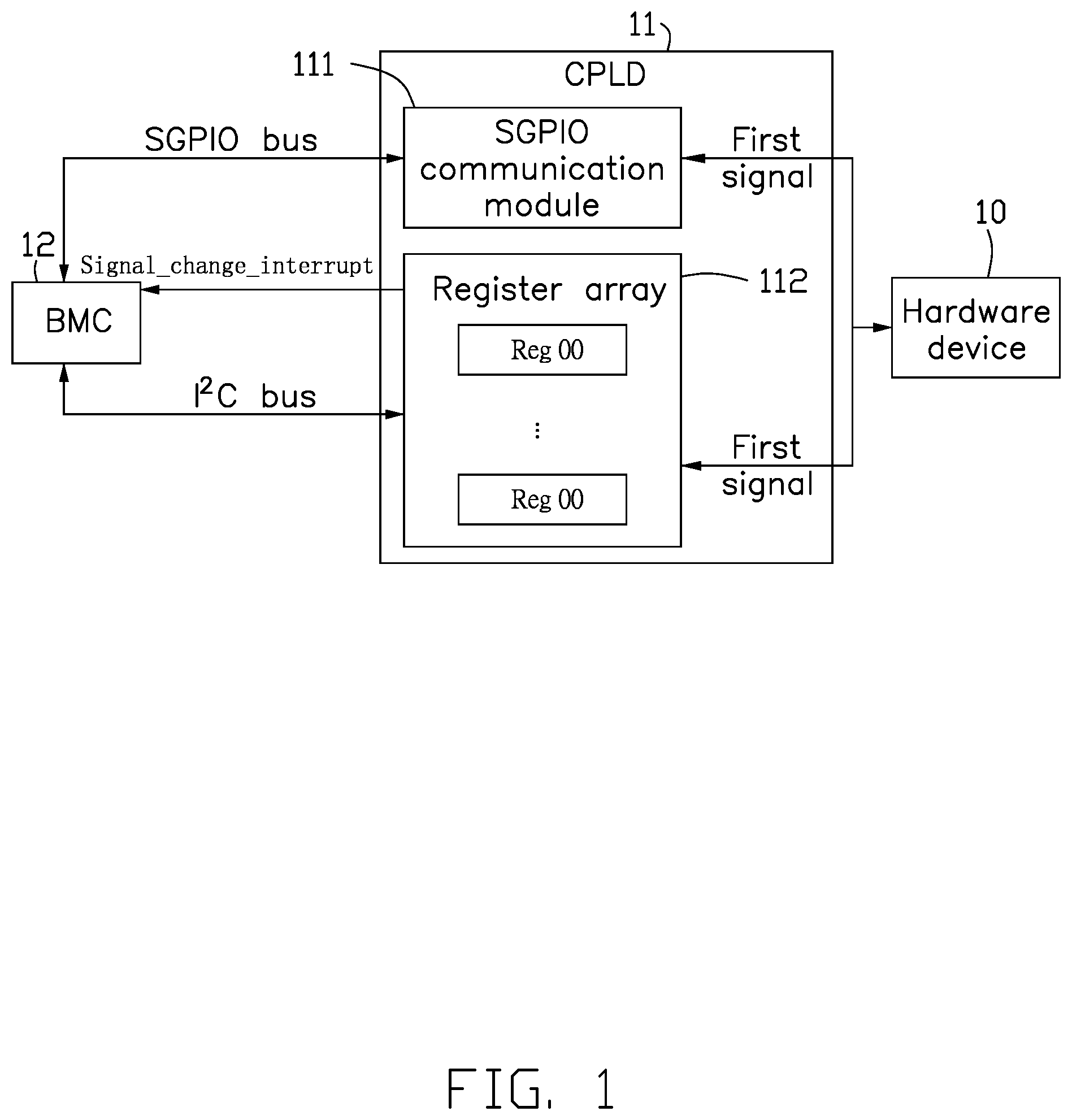
illustrates a communication structure between a baseboard management controller (BMC) and a complex programmable logic device (CPLD).
In the embodiment, a hardware device 10 is connected to a CPLD 11 , and the CPLD is connected to a BMC 12 . The hardware device 10 transmits a first signal to the CPLD 11 , and the BMC 12 reads the first signal from the CPLD 11 . The first signal includes the chassis, the fan, the memory, the processor, the system information, the temperature, the voltage, the board position information, the LED state, the system startup, the shutdown, the reset and other relevant information on the server.
In the embodiment, the BMC 12 is an independent service processor used to manage and monitor each hardware device 10 in the server, for example, including error query, error warning, error reporting and error isolation of the hardware device 10 .
In the embodiment, the CPLD 11 is integrated on the motherboard of the server, and the first signal is obtained by the CPLD 11 , so as to realize the related functions of on-off timing control, key de-jitter, signal delay and indicator control.
In the embodiment, the CPLD 11 includes a serial general-purpose input/output (SGPIO) communication module 111 and a register array 112 . The SGPIO communication module 111 can store the first signal. The SGPIO communication module 111 is connected to the BMC 12 through the SGPIO bus. The BMC 12 can obtain the first signal from the SGPIO communication module 111 through the SGPIO bus.
The register array 112 stores the first signal. The register array 112 is connected to the BMC 12 through the I 2 C bus. As shown in , the register array 112 may include 30 registers from Reg 00 to Reg 29 . The CPLD 11 is set as I 2 C slave, such as the register array 112 is used as I 2 C slave. The BMC 12 (as I 2 C host) can communicate with I 2 C slave through I 2 C bus, that is, the BMC 12 can read and write the first signal on the register array 112 through I 2 C bus.
is a flowchart of a communication method between the BMC and the CPLD. The communication method includes the following steps:
At step S 21 , the CPLD 11 obtains the first signal transmitted by the hardware device 10 .
At step S 22 , the CPLD 11 transmits the first signal to the SGPIO communication module 111 .
At step S 23 , the BMC 12 reads the first signal from the SGPIO communication module 111 through the SGPIO bus.
At step S 24 , the CPLD 11 transmits the first signal to the register array 112 .
In the embodiment, the register array 112 serves as the I 2 C slave, and the CPLD 11 stores the first signal to the register array 112 , so that the BMC 12 , as the I 2 C master, can communicate with the I 2 C slave through the I 2 C bus, and read and write the first signal on the register array 112 .
At step S 25 , the CPLD 11 determines whether the first signal changes. If the first signal changes, step S 26 is implement, otherwise, step S 27 is implement.
At step S 26 , the register array 112 outputs the interrupt signal (the signal_change_interrupt as shown in ) to the BMC 12 , so that the BMC 12 can immediately read the first signal through the I 2 C bus, such as the BMC 12 immediately polls the registers Reg 00 to Reg 29 in the register array 112 through the I 2 C bus to read the first signal.
At step S 27 , the BMC 12 polls the register array 112 through the I 2 C bus.
The BMC 12 communicates with the CPLD 11 to better monitor and manage the server. The communication mode between the BMC 12 and the CPLD 11 directly affects the real-time and reliability of the BMC 12 monitoring server.
The above SGPIO bus can transmit up to 10 bytes in a single cycle, and the data transmitted in a single cycle is limited. During the serial transmission of the SGPIO bus, some signal changes will occur, and these signal changes may be filtered out and lost. For example, in the first cycle, the SGPIO bus transmits the signal A (such as bit), when other signals continue to be transmitted, the signal A changes. When the SGPIO bus transmits the signal A in the next cycle, the signal A has been recovered, and the information about the change of the signal A is filtered out and lost. When communicating through the SGPIO module, there is no mechanism to solve the problem that signals that change between two cycles cannot be transmitted.
The above I 2 C bus takes a long time to transmit data. is a schematic diagram of the BMC reading bytes from the I 2 C slave. As shown in , take the BMC 12 reading 30 bytes of the data from the CPLD 11 as an example, the BMC 12 reads 1 byte of the data, and needs to transmit 38 bits (waveform). It can be understood that reading 30 bytes of the data requires 1140 bits plus 1 stop bit, a total of 1141 bits. The BMC 12 needs 1141 clocks to fully read 30 bytes of the data. When the BMC 12 normally polls the signal (byte) in the CPLD 11 , the BMC 12 will also read the interrupt signal, which will occupy more resources of the BMC 12 .
In order to solve the above problems, the present disclosure provides another CPLD. Based on the communication between the CPLD and the BMC provided by the embodiment of the present disclosure, it can save the communication time, save the resources of the BMC, and will not lose the signal that changes (jumps) in a short time.
illustrates a communication structure between a BMC and a CPLD in accordance with another embodiment of the present disclosure.
In the embodiment, the hardware device 40 is connected to the CPLD 41 , and the CPLD 41 is connected to the BMC 42 . The hardware device 40 transmits the first signal to the CPLD 41 , and the BMC 42 reads the first signal from the CPLD 41 .
The difference between and is that the CPLD 41 includes a data transmission module 411 , a first input first output (FIFO) memory 412 , and a first register 413 .
The data transmission module 411 is connected to the FIFO memory 412 , and the FIFO memory 412 is connected to the first register 413 . The data transmission module 411 obtains the first signal of the hardware device 40 , transmits the obtained first signal to the FIFO memory 412 , and stores the first signal in the first register 413 by the FIFO memory 412 . The BMC 42 reads the first signal in the first register 413 through the I 2 C bus.
The data transmission module 411 is used to obtain the first signal transmitted by the hardware device 40 to the CPLD and store the first signal. The data transmission module 411 can connect each hardware device 40 through a connecting line, and then obtain the first signal of each hardware device 40 . For example, the data transmission module 411 connects the pins of the processor chip through a connecting line and can directly obtain the first signal output by the processor chip.
In the embodiment, the data transmission module 411 includes a memory 414 , and the memory 414 stores the first signal. The memory 414 is divided into many blocks in advance. The data transmission module 411 performs distributed processing on the first signal and stores it in a block preset by the memory 414 . The memory 414 may be a random-access memory (RAM), for example, distributed RAM or block RAM.
In the embodiment, the memory 414 in the data transmission module 411 is divided into N blocks, and the first signal is stored in the N blocks. The data transmission module 411 sets an index byte for each block, and the index byte is used for the index block. The BMC 42 knows which block of the data is being read according to the index byte. For example, as shown in Table 1, the memory 414 is divided into 6 RAM blocks (Block0˜Block5), each block includes 6 bytes (Byte0˜Byte5).
TABLE 1
Block0 Byte0 (index byte) Byte1 Byte2 Byte3 Byte4 Byte5
Block1 Byte0 (index byte) Byte1 Byte2 Byte3 Byte4 Byte5
Block2 Byte0 (index byte) Byte1 Byte2 Byte3 Byte4 Byte5
Block3 Byte0 (index byte) Byte1 Byte2 Byte3 Byte4 Byte5
Block4 Byte0 (index byte) Byte1 Byte2 Byte3 Byte4 Byte5
Block5 Byte0 (index byte) Byte1 Byte2 Byte3 Byte4 Byte5
Byte0 is the index byte. For example, set index bytes for each RAM block (Block0˜Block5) in Table 1 above, as shown in Table 2.
TABLE 2
Index byte value definition
0x00 Block0
0x01 Block1
0x02 Block2
0x03 Block3
0x04 Block4
0x05 Block5
As can be seen from Table 2, if the index byte value read in Byte0 is 0x00, it indicates that the block currently read is Block0 if the index byte value read in Byte0 is 0x05, it indicates that the currently read block is Block5.
In the embodiment, the data transmission module 411 further includes an edge detection module 415 , the edge detection module 415 communicates with the memory 414 , and the edge detection module 415 can access the data stored in the memory 414 . The edge detection module 415 is used to detect whether the first signal changes. The change of the first signal can be the change of the first signal stored by the data transmission module 411 . For example, if the edge detection module 415 detects the edge of the signal from high level to low level, or the edge detection module 415 detects the edge of the signal from low level to high level, it is determined that the signal changes, and the edge detection module 415 outputs an enable signal (such as signal_change in ), the enable signal is used to indicate the change of the first signal.
In the embodiment, the data transmission module 411 includes an input terminal A 1 , an output terminal A 2 and a write control terminal A 3 . The input terminal A 1 is used to receive the first signal of the hardware device 40 , the output terminal A 2 is used to output the first signal, and the write control terminal A 3 is used to output the enable signal.
The first register 413 has the functions of receiving signals, storing signals and outputting signals. The first register 413 can be implemented as an I 2 C slave, and the first register 413 is used to communicate with the BMC 42 through the I 2 C bus.
For example, the first register 413 can be an 8-bit register (such as 8-bit Reg 00 in ).
The first register 413 includes a first port B 1 , a second port B 2 and a read control terminal B 3 . The first port B 1 is used to receive the first signal, the second port B 2 is used to output the first signal, and the read control terminal B 3 is used to output the read signal (for example, BMC_I 2 C_read in ).
The FIFO memory 412 is used to store the first signal. The FIFO memory 412 is a first-come-first-served service mode: the work in the queue will be completed first, and the work in the queue must wait.
For example, the FIFO memory 412 stores bytes as shown in Table 3.
TABLE 3
Byte n
. . .
Byte 23 Block0 Byte5
Byte 22 Block0 Byte4
Byte 21 Block0 Byte3
Byte 20 Block0 Byte2
Byte 19 Block0 Byte1
Byte 18 Block0 Byte0
(index byte 0x00)
Byte 17 Block2 Byte5
Byte 16 Block2 Byte4
Byte 15 Block2 Byte3
Byte 14 Block2 Byte2
Byte 13 Block2 Byte1
Byte 12 Block2 Byte0
(index byte 0x02)
Byte 11 Block3 Byte5
Byte 10 Block3 Byte4
Byte 09 Block3 Byte3
Byte 08 Block3 Byte2
Byte 07 Block3 Byte1
Byte 06 Block3 Byte0
(index byte 0x03)
Byte 05 Block2 Byte5
Byte 04 Block2 Byte4
Byte 03 Block2 Byte3
Byte 02 Block2 Byte2
Byte 01 Block2 Byte1
Byte 00 Block2 Byte0
(index byte 0x02)
As can be seen from Table 3, the number of bytes stored in the FIFO memory 412 is variable. The edge detection module 415 in the data transmission module 411 detects that the signal in the memory 414 has changed, and then transmits the block of the changed signal to the FIFO memory 412 . If the signal in a block changes continuously, the data transmission module 411 can store 6 bytes in the block (such as Block2) into the FIFO byte for many times. Take the FIFO memory 412 can store 30 bytes as an example, Byte n in Table 3 can be Byte 29.
In the embodiment, the FIFO memory 412 includes a data input port C 1 , a data output port C 2 , a write permission port C 3 , a read permission port C 4 , and a FIFO state port C 5 . The data input port C 1 is used to receive data (such as the first signal, that is, the changed signal). In some embodiments, the data input port C 1 is used to receive the block where the first signal is located, for example, if Byte 2 and Byte 3 in Block 2 change, the whole Block 2 will be transferred to the FIFO memory 412 . The data output port C 2 is used to output the data stored in the FIFO memory 412 (such as the first signal that changes). The write permission port C 3 is used to control the write operation of the FIFO memory 412 . The read permission port C 4 is used to control the read operation of the FIFO memory 412 . The FIFO state port C 5 outputs the current state of the FIFO memory 412 , as shown in , a full-state signal FIFO_almost_full, an empty state signal FIFO_empty).
The input terminal A 1 of the data transmission module 411 is connected to the hardware device 40 , and the output terminal A 2 of the data transmission module 411 is connected to the data input port C 1 of the FIFO memory 412 . The write control terminal A 3 of the data transmission module 411 is connected to the write permission port C 3 of the FIFO memory 412 , the data output port C 2 of the FIFO memory 412 is connected to the first port B 1 of the first register 413 . The read permission port C 4 of the FIFO memory 412 is connected to the read control terminal B 3 of the first register 413 , the FIFO state port C 5 of the FIFO memory 412 is connected to the first terminal D 1 of the BMC 42 , the second port B 2 of the first register 413 is connected to the second terminal D 2 of the BMC 42 .
In the embodiment, the data transmission module 411 receives the first signal of the hardware device 40 through the input terminal A 1 . When the data transmission module 411 detects the change of the first signal in the memory 414 , the data transmission module 411 outputs the enable signal (signal_change) through the write control terminal A 3 to the write permission port C 3 of the FIFO memory 412 , after the write permission port C 3 of the FIFO memory 412 receives the enable signal (signal_change), the FIFO memory 412 can allow the data transmission module 411 to write data (such as the block corresponding to the first signal) to the FIFO memory 412 . The data transmission module 411 transmits the block corresponding to the first signal to the data input port C 1 of the FIFO memory 412 through the output terminal A 2 , or, when powering on, the data transmission module 411 outputs the enable signal (signal_change) through the write control terminal A 3 to the write permission port C 3 of the FIFO memory 412 , thereby allowing the data transmission module 411 to write data to the FIFO memory 412 . When powering on, the BMC 42 transmits the I 2 C slave address to the corresponding I 2 C slave, so that the corresponding I 2 C slave reads data from the FIFO memory 412 .
The FIFO memory 412 outputs the full-state signal FIFO_almost_Full and the empty state signal FIFO_empty to the first terminal D 1 of the BMC through the FIFO state port C 5 . If the BMC 42 receives the empty state signal FIFO_empty, the BMC 42 is in an idle state, it does not call the I 2 C bus to read the first signal in the first register 413 . If the BMC 42 receives the full-state signal FIFO_almost_full, the BMC 42 immediately calls the I 2 C bus to read the first signal in the first register 413 , that is, the block where the first signal is located, the first register 413 outputs the read signal (BMC_I 2 C_read) through the read control terminal B 3 to the read permission port C 4 of the FIFO memory 412 , after the FIFO memory 412 receives the read signal (BMC_I 2 C_read), it can allow the first register 413 to read data (such as the first signal or the block where the first signal is located) from the FIFO memory 412 through the first port B 1 . After the first register 413 reads the data, the BMC 42 can read the data from the first register 413 . If the BMC 42 does not receive the full-state signal FIFO_almost_full and the empty state signal FIFO_empty, the BMC 42 can know that the FIFO memory 412 is not full.
is a flowchart of a communication method between the BMC and the CPLD in accordance with an embodiment of the present disclosure. The communication method includes the following steps:
At step S 51 , the server starts to power on.
At step S 52 , the data transmission module 411 transmits the received first signal to the FIFO memory 412 .
In the embodiment, when the server is powered on, the data transmission module 411 places the first signal or the block where the first signal is located in the FIFO memory 412 in sequence, the FIFO memory 412 is a first-come-first-served service mode: the work in the queue will be completed first, and the work in the queue must wait, therefore, the BMC 42 always reads the outermost byte of the FIFO memory 412 first.
At step S 53 , the FIFO memory 412 transmits the first signal to the first register 413 .
In the embodiment, when the server is powered on, the data transmission module 411 transmits all the first signals obtained to the FIFO memory 412 .
In some embodiments, the data transmission module 411 transmits the whole block of the first signal obtained to the FIFO memory 412 .
At step S 54 , the BMC 42 reads the first signal on the first register 413 through the I 2 C bus.
In the embodiment, when the server is powered on, the BMC 42 will poll the CPLD 41 through the I 2 C bus, and the CPLD 41 will transfer almost all information of the FIFO memory 412 to the BMC 42 .
The BMC 42 reads the first signal on the first register 413 through the I 2 C bus, including the following steps:
At step 1 , the BMC 42 transmits the I 2 C slave address to the corresponding I 2 C slave.
The BMC 42 transmits the slave address (such as 0001xx0) of the I 2 C slave on the CPLD 41 to the I 2 C slave (the first register 413 ) on the CPLD 41 .
At step 2 , the I 2 C slave responds to the I 2 C slave address and transmits the read signal to the FIFO memory 412 .
After the first register 413 receives the I 2 C slave address belonging to it, the first register 413 outputs the read signal (BMC_I 2 C_read) to the FIFO memory 412 .
At step 3 , the FIFO memory 412 transmits the obtained first signal to the first register 413 .
After receiving the read signal from the FIFO memory 412 , the first register 413 is allowed to read the first signal or read the block of the first signal from the FIFO memory 412 in turn, and the first register 413 first reads the data stored in the FIFO 412 by the data transmission module 411 . For example, if the first stored data Byte 00 in Table 3 is Block2 Byte® (index byte 0x02), the first register 413 reads and retrieves Block2 Byte® first, and then reads and retrieves Block2 Byte1, until the data corresponding to Byte n is read.
At step 4 , the BMC 42 reads the first signal on the I 2 C slave through the I 2 C bus.
The BMC 42 reads the first signal or the block of the first signal on the first register 413 through the I 2 C bus.
At step S 55 , the BMC 42 determines whether the first signal has been read. If the first signal has been read, step S 56 is implement, otherwise returns to step S 54 .
If the first register 413 has read the first signal in the FIFO memory 412 , the FIFO memory 412 will output the empty state signal FIFO_empty to the BMC 42 . If the BMC 42 does not receive the empty state signal FIFO_empty, the BMC 42 determines that the first signal has not been read.
At step S 56 , the BMC 42 is in idle state.
The BMC 42 receives the empty state signal FIFO_empty output by the FIFO memory 412 , the BMC 42 will no longer call the I 2 C bus to read the first signal on the first register 413 ,
If the first signal has not been read, the BMC 42 continues to read the first signal or the block of the first signal on the first register 413 through the I 2 C bus.
At step S 57 , the data transmission module 411 determines whether the first signal changes. If the data transmission module 411 determines that the first signal changes, step S 58 is implement, otherwise returns to step S 56 .
At step S 58 , the data transmission module 411 transmits the changed first signal or the block corresponding to the first signal to the FIFO memory 412 .
For example, if the data transmission module 411 detects that a signal of Byte2 in Block2 changes from high to low, the data transmission module 411 transfers Byte0 to Byte5 bytes in Block2 to the FIFO memory 412 .
In the embodiment, the data of the block in the data transmission module 411 is put into the FIFO memory 412 in the following two cases:
Case 1 : when the server is powered on for the first time, all blocks in the data transmission module 411 will be placed in the FIFO memory 412 in sequence.
Case 2 : When the data (such as a bit) in a block (such as Block2) in the data transmission module 411 is changed, the data (such as Byte0˜Byte5 in Block2) in this block (Block2) are written into the FIFO memory 412 .
At step S 59 , the FIFO memory 412 determines whether the current storage will be full. If the FIFO memory 412 determines that the current memory will be full, step S 60 is implement, otherwise step S 61 is implement.
At step S 60 , the FIFO memory 412 outputs the full-state signal FIFO_almost_full to the BMC 42 to enable the BMC 42 to read the first signal immediately through the I 2 C bus.
The FIFO memory 412 can store up to 30 bytes, and can also store up to 10 bytes, which is not specifically limited in this disclosure. If the FIFO memory 412 can store up to 30 bytes, when the FIFO memory 412 has stored 29 bytes of data, the FIFO memory 412 outputs the full-state signal FIFO_almost_full to the BMC 42 .
At step S 61 , the FIFO memory 412 determines whether it is currently empty. If the FIFO memory 412 determines that it is currently empty, step S 62 is implement, otherwise step S 63 is implement.
At step S 62 , the FIFO memory 412 outputs empty state signal FIFO_empty to the BMC 42 to keep the BMC 42 in an idle state.
At step S 63 , the BMC 42 polls the first signal on the first register 413 through the I 2 C bus.
Referring to , if the FIFO memory 412 is empty, it means that the BMC 42 does not read data from the CPLD 41 , and the BMC 42 needs 0 clock to read data. If the FIFO memory 412 is not empty, for example, the FIFO memory 412 stores two blocks, the BMC 42 reads two blocks from the CPLD 41 . The BMC 42 reads the data of two blocks, it needs to transmit 1 byte of address (the first register 413 is used as the I 2 C slave), plus 2 bytes of index, plus 10 bytes of data, plus 13 ACK bits, plus 1 start bit, plus 1 stop bit, a total of 119 bits. The BMC needs 119 clocks to fully read 10 bytes of the data.
It can be seen from the above that on the CPLD 41 , the data transmission module 411 has the edge detection function by setting the data transmission module 411 , when the signal changes, the changed signal is transmitted to the FIFO memory 412 , and the BMC 42 can read the changed signal through the FIFO memory 412 , there is no need to poll the register array as shown in , which saves communication time, reduces the resource occupation of the BMC 42 , and does not lose the signal that changes (jumps) in a short time. The present disclosure establishes the communication between the first register 413 and the BMC 42 through the I 2 C bus, it can transmit unlimited bytes in a single cycle. Furthermore, the first register 413 has only one fixed register, so compared with the register array, it only needs to transmit 1 byte of address, further saving communication time.
Those of ordinary skill in the art should realize that the above embodiments are only used to illustrate the present disclosure, but not to limit the present disclosure. As long as they are within the essential spirit of the present disclosure, the above embodiments are appropriately made and changes fall within the scope of protection of the present disclosure.
Figures (6)
Citations
This patent cites (3)
- US10430225
- US2013/0117766
- US2016/0117461