Operation Method of Electronic Device for Sensing Optical Signal and Electronic Device
Abstract
An operation method of an electronic device for sensing an optical signal is provided. The electronic device includes a plurality of optical sensors and a plurality of light-emitting elements disposed adjacent to the plurality of optical sensors. The operation method of the electronic device for sensing the optical signal includes the following steps. The optical signal is provided to a first optical sensor of the plurality of optical sensors. The first optical sensor outputs a driving signal when dimming the plurality of light-emitting elements adjacent to the first optical sensor. Therefore, the accuracy of sensing the optical signal may be effectively increased.
Claims (15)
1. An operation method for sensing an optical signal, comprising: providing an electronic device, wherein the electronic device comprises a plurality of optical sensors and a plurality of light-emitting elements; the plurality of light-emitting elements emitting a first optical signal, wherein the first optical signal has a first gray level; the plurality of light-emitting elements emitting a second optical signal, wherein the second optical signal has a second gray level, and the second gray level and the first gray level are different; providing an object, wherein the object reflects the second optical signal to form a third optical signal; and a first optical sensor of the plurality of optical sensors outputting a driving signal according to the third optical signal; wherein during the detection period, the plurality of light-emitting elements are dimmed, and the first optical signal with the first gray level is adjusted to the second optical signal with the second gray level.
9. An electronic device, comprising: a substrate; a first light-emitting element, disposed on the substrate; a second light-emitting element, disposed on the substrate, wherein the first light-emitting element is adjacent to the second light-emitting element; and an optical sensor, disposed on the substrate, wherein the optical sensor is adjacent to the first light-emitting element and the second light-emitting element; wherein a distance between the optical sensor and the first light-emitting element is less than half of a distance between the first light-emitting element and the second light-emitting element; wherein the first light-emitting element and the second light-emitting element emit a first optical signal, and the first optical signal has a first gray level; wherein the first light-emitting element and the second light-emitting element emit a second optical signal, the second optical signal has a second gray level, and the second gray level and the first gray level are different; wherein during the detection period, the first light-emitting element and the second light-emitting element are dimmed, and the first optical signal with the first gray level is adjusted to the second optical signal with the second gray level.
Show 13 dependent claims
2. The operation method for sensing the optical signal according to claim 1 , wherein the second gray level is lower than the first gray level when the first gray level is a highest gray level of the electronic device.
3. The operation method for sensing the optical signal according to claim 1 , wherein the second optical signal is a pulsed optical signal.
4. The operation method for sensing the optical signal according to claim 1 , wherein the first optical sensor is adjacent to a first light-emitting element and a second light-emitting element of the plurality of light emitting elements.
5. The operation method for sensing the optical signal according to claim 4 , wherein a distance between the first optical sensor and the first light-emitting element is less than half of a distance between the first light-emitting element and the second light-emitting element.
6. The operation method for sensing the optical signal according to claim 4 , wherein a height of the first light-emitting element is higher than a height of the first optical sensor.
7. The operation method for sensing the optical signal according to claim 4 , wherein the first optical sensor is disposed below the first light-emitting element.
8. The operation method for sensing the optical signal according to claim 1 , wherein the first optical signal is an optical signal emitted by the plurality of light-emitting elements during a display period, and the second optical signal is an optical signal emitted by the plurality of light-emitting elements during a detection period.
10. The electronic device according to claim 9 , wherein a height of the first light-emitting element is higher than a height of the optical sensor.
11. The electronic device according to claim 9 , wherein the second optical signal is a pulsed optical signal.
12. The electronic device according to claim 9 , wherein the second gray level is lower than the first gray level when the first gray level is a highest gray level of the electronic device.
13. The electronic device according to claim 9 , wherein the first optical signal is emitted by the first light-emitting element during a display period, and the second optical signal is emitted by the second light-emitting element during a detection period.
14. The electronic device according to claim 9 , wherein the optical sensor outputs a driving signal according to a third optical signal generated by an object reflecting the second optical signal.
15. The electronic device according to claim 9 , wherein the optical sensor is disposed below the first light-emitting element.
Full Description
Show full text →
CROSS REFERENCE TO RELATED APPLICATIONS
This application is a Divisional of U.S. patent application Ser. No. 17/210,914, filed Mar. 24, 2021, which claims priority of China Patent Application No. 202010284110.0, filed on Apr. 13, 2020, the entirety of which is incorporated by reference herein.
CROSS REFERENCE TO RELATED APPLICATIONS
Field of the Disclosure
The present disclosure relates to an operation method, and in particular it relates to an operation method of an electronic device for sensing an optical signal and an electronic device.
DESCRIPTION OF THE RELATED ART
A conventional electronic device may sense light generated by a laser pen, or the reflected light generated by a finger touching an electronic device through an optical sensor, in order to determine the position of the laser pen or the finger on the electronic device. However, since the proper operation of the optical sensor may be affected by ambient light or light with a corresponding brightness that is generated by the light-emitting element of the electronic device, the accuracy of sensing the optical signal may be decreased. Therefore, a new driving design is needed to solve the above problem.
BRIEF SUMMARY OF THE DISCLOSURE
An embodiment of the disclosure provides an operation method of an electronic device for sensing an optical signal. The electronic device includes a plurality of optical sensors and a plurality of light-emitting elements disposed adjacent to the plurality of optical sensors. The operation method of the electronic device for sensing the optical signal includes the following steps. The optical signal is provided to a first optical sensor of the plurality of optical sensors. The first optical sensor outputs a driving signal when dimming the plurality of light-emitting elements adjacent to the first optical sensor.
In addition, an embodiment of the disclosure provides an operation method for sensing an optical signal, which includes the following steps. An electronic device is provided, wherein the electronic device includes a plurality of optical sensors and a plurality of light-emitting elements. The plurality of light-emitting elements emit a first optical signal, wherein the first optical signal has a first gray level. The plurality of light-emitting elements emitting a second optical signal, wherein the second optical signal has a second gray level, and the second gray level and the first gray level are different. An object is provided, wherein the object reflects the second optical signal to form a third optical signal. A first optical sensor of the plurality of optical sensors outputs a driving signal according to the third optical signal.
In addition, an embodiment of the disclosure provides an electronic device, which includes a substrate, a first light-emitting element, a second light-emitting element and an optical sensor. The first light-emitting element is disposed on the substrate. The second light-emitting element is disposed on the substrate, and the first light-emitting element is adjacent to the second light-emitting element. The optical sensor is disposed on the substrate, and the optical sensor is adjacent to the first light-emitting element and the second light-emitting element. The distance between the optical sensor and the first light-emitting element is less than half of the distance between the first light-emitting element and the second light-emitting element.
BRIEF DESCRIPTION OF THE DRAWINGS
The disclosure can be fully understood by reading the subsequent detailed description and examples with references made to the accompanying drawings, wherein:
is a schematic view of an electronic device according to an embodiment of the disclosure;
is an operation timing diagram of an optical sensor and light-emitting elements of an electronic device according to an embodiment of the disclosure;
is an operation timing diagram of an optical sensor and light-emitting elements of an electronic device according to an embodiment of the disclosure;
is a schematic view of an electronic device according to another embodiment of the disclosure;
is a cross-sectional view of the electronic device in taken along a line A-A′;
is a partial cross-sectional view of the electronic device in taken along line A-A′;
is a stereogram of the electronic device in along line A-A′;
is a flowchart of an operation method of an electronic device for sensing an optical signal according to an embodiment of the disclosure; and
is a flowchart of an operation method of an electronic device for sensing an optical signal according to an embodiment of the disclosure.
DETAILED DESCRIPTION OF THE DISCLOSURE
In order to make objects, features and advantages of the disclosure more obvious and easily understood, the embodiments are described below, and the detailed description is made in conjunction with the drawings. In order to help the reader to understand the drawings, the multiple drawings in the disclosure may merely depict a part of the entire device, and the specific components in the drawing are not drawn to scale.
The specification of the disclosure provides various embodiments to illustrate the technical features of the various embodiments of the disclosure. The configuration, quantity, and size of each component in the embodiments are for illustrative purposes only, and are not intended to limit the disclosure. In addition, if the reference number of a component in the embodiments and the drawings appears repeatedly, it is for the purpose of simplifying the description, and does not mean to imply a relationship between different embodiments.
Furthermore, use of ordinal terms such as “first”, “second”, etc., in the specification and the claims to describe a claim element does not by itself connote and represent the claim element having any previous ordinal term, and does not represent the order of one claim element over another or the order of the manufacturing method, either. The ordinal terms are used merely as labels to distinguish one claim element having a certain name from another element having the same name.
In the disclosure, the technical features of the various embodiments may be replaced or combined with each other to complete other embodiments without being mutually exclusive.
is a schematic view of an electronic device according to an embodiment of the disclosure. In some embodiments, the electronic device 100 may include a liquid crystal (LC), an organic light-emitting diode (OLED), a light-emitting diode (LED), a quantum dot (QD), a fluorescence, a phosphor, other suitable materials, or a combination thereof, but the disclosure is not limited thereto. The light-emitting diode may include, for example, a mini light-emitting diode (mini LED), a micro light-emitting diode (micro LED), a quantum dot light-emitting diode (QLED/QDLED). In some embodiments, the electronic device 100 may be a display device, an antenna device, a sensing device, a touch display, a curved display or a free shape display, and may also be a bendable or flexible spliced display device, but the disclosure is not limited thereto. The antenna device may be, for example, a liquid crystal antenna, but the disclosure is not limited thereto. It should be noted that the electronic device may be any combination of the foregoing, but the disclosure is not limited thereto. Furthermore, the appearance of the electronic device may be rectangular, circular, polygonal, a shape with curved edges, or other suitable shapes. The electronic device may include peripheral systems, such as a driving system, a control system, a light source system, a shelf system, etc., to support the display device or the antenna device.
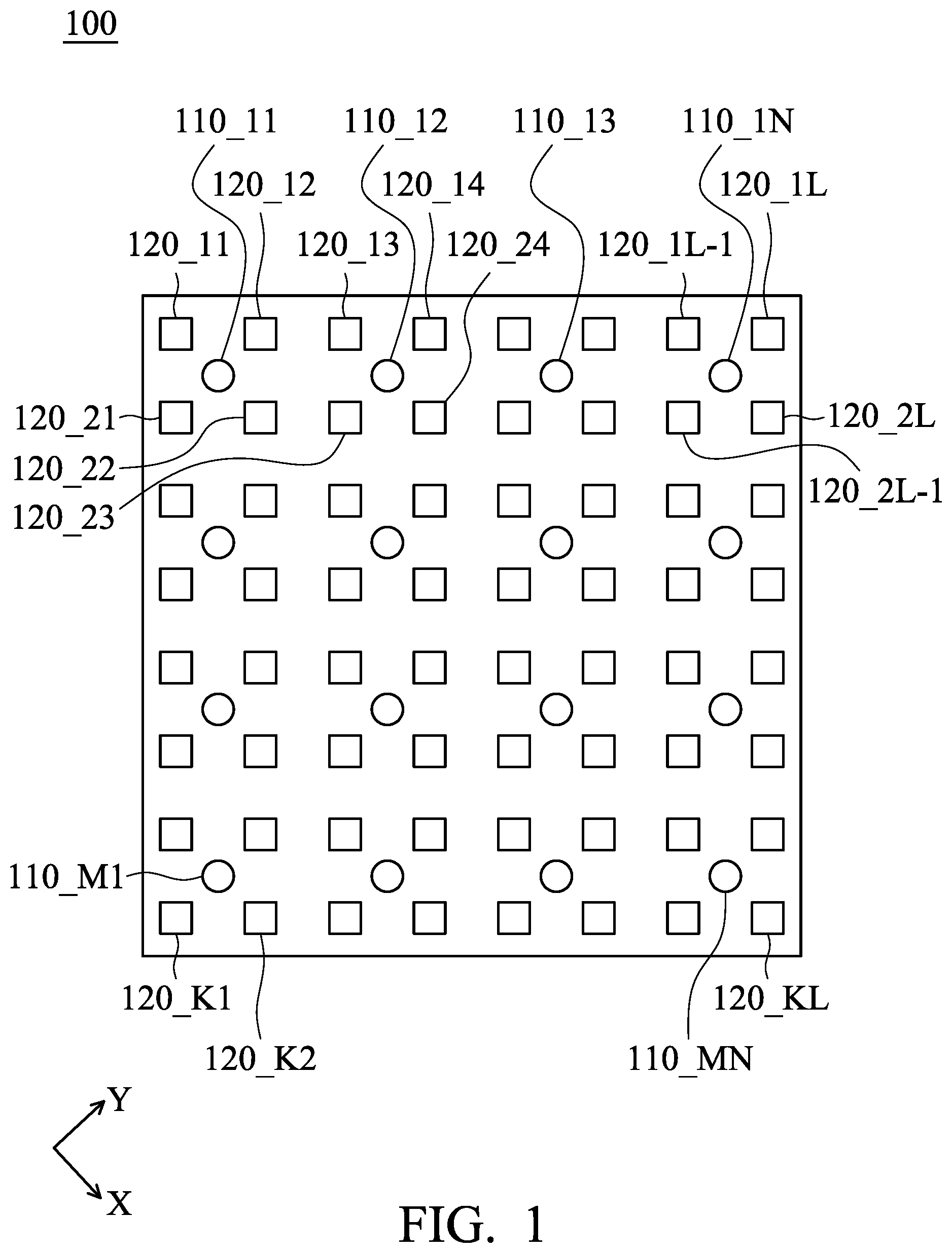
Please refer to . The electronic device 100 may include a plurality of optical sensors 110 _ 11 ˜ 110 _MN and a plurality of light-emitting elements 120 _ 11 ˜ 120 _KL, wherein M, N, K and L are positive integers greater than 1. In the embodiment, K and L are greater than M and N, i.e., a number of light-emitting elements 120 _ 11 ˜ 120 _KL is greater than a number of optical sensors 110 _ 11 ˜ 110 _MN. In some embodiments, M and N may be the same or different, and K and L may be the same or different. In the embodiment, the optical sensor 110 _ 11 ˜ 110 _MN may be made of thin film transistors (TFTs) or other sensors, but the disclosure is not limited thereto. In addition, the optical sensors 110 _ 11 ˜ 110 _MN are used to sense the optical signal generated by the light source device (not shown). The above light source device is, for example, a laser light pen or an infrared light pen, but the disclosure is not limited thereto.
The light-emitting elements 120 _ 11 ˜ 120 _KL may be disposed adjacent to the optical sensors 110 _ 11 ˜ 110 _MN. For example, the light-emitting element 120 _ 11 , the light-emitting element 120 _ 12 , the light-emitting element 120 _ 21 and the light-emitting element 120 _ 22 may be disposed adjacent to the optical sensor 110 _ 11 . That is, for example, there are no other light-emitting elements or optical sensors between the light-emitting element 120 _ 11 and the optical sensor 110 _ 11 , and there are no other light-emitting elements or optical sensors between the light-emitting element 120 _ 12 and the optical sensor 110 _ 11 . The light-emitting element 120 _ 13 , the light-emitting element 120 _ 14 , the light-emitting element 120 _ 23 and the light-emitting element 120 _ 24 may be disposed adjacent to the optical sensor 110 _ 12 . The light-emitting element 120 _ 1 L- 1 , the light-emitting element 120 _ 1 L, the light-emitting element 120 _ 2 L- 1 and the light-emitting element 120 _ 2 L may be disposed adjacent to the optical sensor 110 _ 1 N. The manner in which the remaining light-emitting elements and the remaining optical sensors are disposed adjacent to each other may be deduced by analogy from the description of the above embodiment.
In the embodiment, the light-emitting elements 120 _ 11 ˜ 120 _KL may be the organic light-emitting diode, the light-emitting diode (LED), such as the mini light-emitting diode, the micro light-emitting diode, the quantum dot light-emitting diode, etc., but the disclosure is not limited thereto. In addition, the light-emitting elements 120 _ 11 ˜ 120 _KL may be a light-emitting die or a package form including the light-emitting die. Furthermore, the light-emitting elements 120 _ 11 ˜ 120 _KL may generate lights of a single color, such as a white light, or lights of multiple colors, such as a red light, a green light, a blue light, but the disclosure is not limited thereto.
In the embodiment, the user may operate the light source device to generate the optical signal to the electronic device 100 . That is, the optical signal is provided to a first optical sensor of the optical sensors 110 _ 11 ˜ 110 _MN of the electronic device 100 , such as the optical sensor 110 _ 11 . Then, when the light-emitting elements (such as the light-emitting element 120 _ 11 , the light-emitting element 120 _ 12 , the light-emitting element 120 _ 21 and the light-emitting element 120 _ 22 ) adjacent to the optical sensor 110 _ 1 are dimmed, the optical sensor 110 _ 1 outputs a driving signal, allowing the electronic device 100 to determine the position of the optical signal. In the embodiment, the light-emitting element is dimmed to decrease the gray level of the light-emitting element, for example, to 50% or less of the original gray level. Furthermore, the gray level of the light-emitting element may be decreased to zero, for example, when the light-emitting element is turned off and does not generate an optical signal.
In some embodiments, the electronic device 100 may further include a plurality of detection periods. The detection periods are periods during which the optical sensors 110 _ 11 ˜ 110 _MN detect and are detected by a processing device (not shown) in the electronic device 100 in order to generate corresponding driving signals. At the same time, the light-emitting elements 120 _ 11 ˜ 120 _KL adjacent to the optical sensors 110 _ 11 ˜ 110 _MN may be dimmed during the corresponding detection periods. For example, when the optical sensor 110 _ 11 detects during the detection period, at least one or all of the light-emitting element 120 _ 11 , the light-emitting element 120 _ 12 , the light-emitting element 120 _ 21 and the light-emitting element 120 _ 22 may be dimmed during the corresponding detection period. When the optical sensor 110 _ 12 detects during the detection period, at least one or all of the light-emitting element 120 _ 13 , the light-emitting element 120 _ 14 , the light-emitting element 120 _ 23 and the light-emitting element 120 _ 24 may be dimmed during the corresponding detection period. The operation of the remaining light-emitting elements and the remaining optical sensors may be deduced by analogy from the description of the above embodiment.
In some embodiments, the optical sensors 110 _ 11 ˜ 110 _MN may detect in order, but the disclosure is not limited thereto. For example, the detective order may be the optical sensor 110 _ 11 , the optical sensor 110 _ 12 , the optical sensor 110 _ 13 , . . . . In addition, the detective order may also be the optical sensors 110 _ 11 ˜ 110 _ 1 N, the optical sensors 110 _ 21 ˜ 110 _ 2 N, the optical sensors 110 _ 31 ˜ 110 _ 3 N, . . . .
In some embodiments, the optical sensors 110 _ 11 ˜ 110 _MN may detect in a skippingly order, but the disclosure is not limited thereto. For example, the detective order may be the optical sensor 110 _ 11 , the optical sensor 110 _ 13 , the optical sensor 110 _ 15 , . . . . In addition, the detective order may also be the optical sensors 110 _ 11 ˜ 110 _ 1 N, the optical sensors 110 _ 31 ˜ 110 _ 3 N, the optical sensors 110 _ 51 ˜ 110 _ 5 N, . . . .
In some embodiments, the optical sensors 110 _ 11 ˜ 110 _MN may detect in an irregular order, but the disclosure is not limited thereto. For example, the detective order may be the optical sensor 110 _ 11 , the optical sensor 110 _ 23 (not marked), the optical sensor 110 _ 41 (not marked), . . . . In addition, the detective order may also be the optical sensors 110 _ 11 ˜ 110 _ 1 N, the optical sensors 110 _ 51 ˜ 110 _ 5 N (not marked), the optical sensors 110 _ 21 ˜ 110 _ 2 N (not marked).
In some embodiments, all of the optical sensors 110 _ 11 ˜ 110 _MN may detect during a detection period, and generate the corresponding driving signals. At the same time, all of the light-emitting elements 120 _ 11 ˜ 120 _KL are dimmed during the detection period. Therefore, the possibility that the optical sensors 110 _ 11 ˜ 110 _MN will mistakenly determine that the light emitted by the adjacent light-emitting elements 110 _ 11 ˜ 110 _MN is the optical signal generated by the light source device may be effectively decreased, effectively increasing the detection accuracy of the optical sensors 110 _ 11 ˜ 110 _MN.
is an operation timing diagram of an optical sensor and light-emitting elements of an electronic device according to an embodiment of the disclosure. For the convenience of description, the electronic device 100 including the optical sensor 110 _ 11 , the light-emitting element 120 _ 11 , the light-emitting element 120 _ 12 , the light-emitting element 120 _ 21 and the light-emitting element 120 _ 22 is taken as an example. The electronic device 100 may include, for example, a frame period F 11 , a frame period F 12 , a frame period F 21 and a frame period F 22 during a display period. The frame period F 11 may include a light-emitting period L 11 and a non-light-emitting period N 11 of the light-emitting element 120 _ 11 or the light-emitting element 120 _ 12 . In an embodiment of the disclosure, the non-light-emitting period N 11 may include a blanking period. In other words, for example, before the frame period F 11 enters the frame period F 12 , the light-emitting element 120 _ 11 or the light-emitting element 120 _ 12 may not receive a gate signal generated by the electronic device 100 for a period, and this period that the gate signal is not received is called the blanking period. The frame period F 12 follows the frame period F 11 , and the frame period F 12 may include a light-emitting period L 12 and a non-light-emitting period N 12 of the light-emitting element 120 _ 11 or the light-emitting element 120 _ 12 . In an embodiment of the disclosure, the non-light-emitting period N 12 may include the blanking period.
The frame period F 21 follows the light-emitting period L 11 of the light-emitting element 120 _ 11 or the light-emitting element 120 _ 12 , and the frame period F 21 may include a light-emitting period L 21 and a non-light-emitting period N 21 of the light-emitting element 120 _ 21 or the light-emitting element 120 _ 22 . In an embodiment of the disclosure, the non-light-emitting period N 21 may include the blanking period. The frame period F 22 follows the frame period F 21 , and the frame period F 22 may include a light-emitting period L 22 and a non-light-emitting period N 22 of the light-emitting element 120 _ 21 or the light-emitting element 120 _ 22 . In an embodiment of the disclosure, the non-light-emitting period N 12 may include the blanking period.
During the light-emitting period L 11 of the frame period F 11 , the light-emitting element 120 _ 11 and the light-emitting element 120 _ 12 may be turned on and emit a light. Then, during the light-emitting period L 21 of the frame period F 21 , the light-emitting element 120 _ 21 and the light-emitting element 120 _ 22 may be turned on and emit a light. At this time, the optical sensor 110 _ 11 may sense the optical signals generated by the light-emitting element 120 _ 11 , the light-emitting element 120 _ 12 , the light-emitting element 120 _ 21 and the light-emitting element 120 _ 22 and generate a driving signal. However, during the frame period F 11 and the frame period F 21 , the driving signal has not yet been detected by the processing device.
During the light-emitting period L 12 of the frame period F 12 , the light-emitting element 120 _ 11 and the light-emitting element 120 _ 12 are dimmed or turned off, i.e., the brightness of the light-emitting element 120 _ 11 and the light-emitting element 120 _ 12 is decreased. For example, the brightness of the light-emitting element 120 _ 11 and the light-emitting element 120 _ 12 is decreased to 50% or less of the original brightness (or the gray level value). Then, during the light-emitting period L 22 of the frame period F 22 , the light-emitting element 120 _ 21 and the light-emitting element 120 _ 22 are dimmed or turned off. In an overlap period of the light-emitting period L 12 and the light-emitting period L 22 , i.e., a detection period T 1 , the optical sensor 110 _ 11 may sense the optical signal generated by the light source device and generate the corresponding driving signal accordingly. The driving signal generated by the optical sensor 110 _ 11 may be transmitted, for example, to the processing device of the electronic device 100 , allowing the processing device to determine the position of the optical signal and perform the corresponding process.
In , the detection period T 1 is between one-half of the light-emitting period L 12 and one-half of the light-emitting period L 22 , but the disclosure is not limited thereto. In another embodiment, the detection period T 1 may be between the starting position of the light-emitting period L 12 and the ending position of the light-emitting period L 22 .
During the non-light-emitting period N 12 of the frame period F 12 , i.e., the blanking period of the light-emitting element 120 _ 11 and the light-emitting element 120 _ 12 , the light-emitting element 120 _ 11 and the light-emitting element 120 _ 12 do not emit the light. Then, during the non-light-emitting period N 22 of the frame period F 22 , i.e., the blanking period of the light-emitting element 120 _ 21 and the light-emitting element 120 _ 22 , the light-emitting element 120 _ 21 and the light-emitting element 120 _ 22 do not emit the light. In an overlap period of the non-light-emitting period N 12 and the non-light-emitting period N 22 (such as an overlap period of the blanking period of the light-emitting element 120 _ 11 and the light-emitting element 120 _ 12 and the blanking period of the light-emitting element 120 _ 21 and the light-emitting element 120 _ 22 ), i.e., a detection period T 2 , the optical sensor 110 _ 11 may sense the optical signal generated by the light source device and generate the corresponding driving signal accordingly. The driving signal generated by the optical sensor 110 _ 11 may be transmitted, for example, to the processing device of the electronic device 100 , allowing the processing device to determine the position of the optical signal and perform the corresponding process. The operation of the remaining optical sensors 110 _ 12 ˜ 110 _MN may be deduced by analogy from the operation of the above optical sensor 110 _ 11 , and the description thereof is not repeated herein.
Therefore, during the light-emitting period of the frame period in which the light-emitting elements are dimmed (for example, the overlap period of the light-emitting period L 12 in which the light-emitting element 120 _ 11 or the light-emitting element 120 _ 12 is dimmed and the light-emitting period L 22 in which the light-emitting element 120 _ 21 or the light-emitting element 120 _ 22 is dimmed) or the non-light-emitting period of the light-emitting elements (for example, the overlap period of the non-light-emitting period N 12 of the light-emitting element 120 _ 11 or the light-emitting element 120 _ 12 and the non-light-emitting period N 22 of the light-emitting element 120 _ 21 or the light-emitting element 120 _ 22 ), the optical sensor 110 _ 11 may sense the optical signal generated by the light source device, so as to effectively decrease the possibility of noise misjudgment or increase the detection accuracy of the optical sensor 110 _ 11 .
In addition, in some embodiments, in cases where the display frame of the electronic device 100 includes the frame with brightest and darkest (such as displaying a fireworks frame), when the optical signal generated by the light source device appears in the darkest position, the optical sensor may immediately sense the optical signal generated by the light source device to generate the corresponding driving signal. When the optical signal generated by the light source device appears in the brightest position, the optical sensor may use the above method to sense, so as to generate the corresponding driving signal. For example, the light-emitting element is dimmed, the optical sensor may sense the brightness of the optical signal generated by the light source device to generate the corresponding driving signal.
is an operation timing diagram of an optical sensor and light-emitting elements of an electronic device according to another embodiment of the disclosure. Please refer to and . The electronic device 100 of the embodiment is the same as the above embodiment, and the description thereof is not repeated herein. For the convenience of description, the electronic device 100 including the optical sensor 110 _ 11 , the light-emitting element 120 _ 11 , the light-emitting element 120 _ 12 , the light-emitting element 120 _ 21 and the light-emitting element 120 _ 22 is taken as an example. The operation of the remaining optical sensors 110 _ 12 ˜ 110 _MN may be deduced by analogy from the operation of the above optical sensor 110 _ 11 , and the description thereof is not repeated herein. The electronic device 100 includes, for example, a frame period F 11 , a frame period F 12 , a frame period F 21 and a frame period F 22 during the display period. The frame period F 11 may include light-emitting periods L 11 and non-light-emitting periods N 11 of a plurality of light-emitting elements, for example, a light-emitting period L 11 and a non-light-emitting period N 11 of the light-emitting element 120 _ 11 or the light-emitting element 120 _ 12 . The frame period F 12 follows the frame period F 11 , and the frame period F 12 may include light-emitting periods L 12 and non-light-emitting periods N 12 of the light-emitting elements.
The frame period F 21 may include light-emitting periods L 21 and non-light-emitting periods N 21 of the light-emitting elements, for example, a light-emitting period L 21 a non-light-emitting period N 21 of the light-emitting element 120 _ 21 or the light-emitting element 120 _ 22 . The frame period F 22 follows the frame period F 21 , and the frame period F 22 may include light-emitting periods L 22 and non-light-emitting periods N 22 of the light-emitting elements. In the embodiment, F 11 , F 12 , F 21 and F 22 are, for example, the frame periods of the electronic device 100 in the display stage.
In the embodiment, the light-emitting element 120 _ 11 , the light-emitting element 120 _ 12 , the light-emitting element 120 _ 21 and the light-emitting element 120 _ 22 normally perform the function of the electronic device 100 during the frame periods F 11 and F 21 , respectively. This function may be, for example, displaying dynamic or static frames. During the next frame period F 12 and the frame period F 22 , the brightness of the light-emitting period L 12 and the light-emitting period L 22 is decreased. At this time, the light-emitting period L 12 and the light-emitting period L 22 are added to form a detection period T 3 . The processing device of the electronic device 100 may receive the driving signal generated by the optical sensor 110 _ 11 during the detection period T 3 and perform the corresponding process. For example, the processing device determines the coordinates of the position of the electronic device 100 that is touched by the finger using the detected driving signal.
In the embodiment, the brightness may also be transformed into a corresponding gray level value to indicate that the gray level value is high or the brightness is high. For example, when the electronic device 100 is performing a function normally, the highest brightness appears, for example, to be gray level 255 . When the processing device receives the driving signal during the detection period T 3 , the electronic device 100 sends a signal, such as a pulsed signal, to the light-emitting element 120 _ 11 , the light-emitting element 120 _ 12 , the light-emitting element 120 _ 21 and the light-emitting element 120 _ 22 . The light-emitting element 120 _ 11 , the light-emitting element 120 _ 12 , the light-emitting element 120 _ 21 and the light-emitting element 120 _ 22 generate a lower gray level during the corresponding light-emitting periods L 12 and L 22 . For example, the light-emitting brightness with the highest brightness of the gray level 255 is taken as an example, the light-emitting elements are adjusted to a relatively lower brightness of the gray level 190 , the noise signal received by the processing device from the driving signal not generated by the optical sensor 110 _ 11 may be decreased, so as to improve the signal-to-noise ratio (SNR) or increase the detection accuracy of the processing device.
In the embodiment, the pulsed signal refers to a periodic signal, but the time axis of the previous signal and the next signal is not continuous. The type of the pulsed signal is not limited. For example, the pulsed signal may be a rectangular pulse, a square wave pulse, a triangular pulse or other suitable pulse signals. It should be noted that decreasing the brightness of light-emitting period L 12 and light-emitting period L 22 and receiving the driving signal generated by the optical sensor 110 _ 11 during the detection period T 3 is an example of the disclosure.
In another embodiment, the brightness of the light-emitting element 120 _ 11 , the light-emitting element 120 _ 12 , the light-emitting element 120 _ 21 and the light-emitting element 120 _ 22 may be increased during the detection period, so that the processing device of the electronic device 100 receives the driving signal generated by the optical sensor 110 _ 11 . For example, referring to , the frame period F 13 and the frame period F 23 are the period that the electronic device 100 normally performs the function. When the processing device starts to detect, the electronic device 100 sends a signal, such as a pulsed signal, such that the brightness of the light-emitting element 120 _ 11 , the light-emitting element 120 _ 12 , the light-emitting element 120 _ 21 and the light-emitting element 120 _ 22 during the corresponding light-emitting period L 13 and light-emitting period L 23 is higher than the brightness of the light-emitting element 120 _ 11 , the light-emitting element 120 _ 12 , the light-emitting element 120 _ 21 and the light-emitting element 120 _ 22 during the previous frame period F 12 . At this time, the added time of the light-emitting period L 13 and the light-emitting period L 23 may be a detection period T 4 , and the processing device may receive the driving signal generated by the optical sensor 110 _ 11 during the detection period T 4 and perform the corresponding process.
Therefore, the brightness of the light-emitting elements during the detection period is changed, such that the optical sensor 110 _ 11 may be detected by the processing device during the light-emitting period of the frame period of the electronic device 100 , so as to effectively decrease the possibility of noise misjudgment or increase the detection accuracy of the processing device. As for the details and steps of the detection may be described in the subsequent embodiments.
is a schematic view of an electronic device according to another embodiment of the disclosure. is a cross-sectional view of the electronic device in taken along a line A-A′. Please refer to and . The electronic device 400 may include a plurality of light-emitting element and a plurality of optical sensors, as shown in the electronic device 100 . It is worth noting that, for the convenience of description, shows a part of the situation of the electronic device. Please refer to . The electronic device 400 at least includes a substrate 410 , a light-emitting element 120 _ 11 , a light-emitting element 120 _ 12 , a light-emitting element 120 _ 21 , a light-emitting element 120 _ 22 and an optical sensor 440 . In an embodiment, the electronic device 400 may be a display device, but the disclosure is not limited thereto. In addition, the light-emitting element 120 _ 11 , the light-emitting element 120 _ 12 , the light-emitting element 120 _ 21 , the light-emitting element 120 _ 22 and the optical sensor 440 shown in and are an exemplary embodiment of the disclosure, but not used to limit the number or shape of light-emitting elements and optical sensor of the disclosure. The user may adjust the number or shape of the light-emitting elements and optical sensor according to the requirements thereof. The disposing of the light-emitting elements and the optical sensor may not necessarily follow the disposing manner shown in . The light-emitting element 120 _ 11 and the light-emitting element 120 _ 21 may be alternatively disposed on the Y direction or other suitable design manners, as long as the effect of the disclosure may be achieved.
In the embodiment, the substrate 410 may be a rigid substrate or a flexible substrate. The material of the substrate includes, for example, glass, quartz, sapphire, polyimide (PI), polycarbonate (PC) or polyethylene terephthalate (PET) or a combination thereof but the disclosure is not limited thereto. The light-emitting element 120 _ 11 , the light-emitting element 120 _ 12 , the light-emitting element 120 _ 21 and the light-emitting element 120 _ 22 are disposed on the substrate 410 , and the light-emitting element 120 _ 11 is adjacent to the light-emitting element 120 _ 22 . In the embodiment, the light-emitting element 120 _ 11 , the light-emitting element 120 _ 12 , the light-emitting element 120 _ 21 and the light-emitting element 120 _ 22 may be the OLED, the LED, such as the mini LED, the micro LED, the QLED/QD-LED etc., but the disclosure is not limited thereto.
The optical sensor 440 is disposed on the substrate 410 and adjacent to the light-emitting element 120 _ 11 and the light-emitting element 120 _ 22 . In the embodiment, the distance D 1 between the optical sensor 440 and the light-emitting element 120 _ 11 is less than half of the distance D 2 between the light-emitting element 120 _ 11 and the light-emitting element 120 _ 22 . That is, the optical sensor 440 is disposed adjacent to the light-emitting element 120 _ 11 and far away from the light-emitting element 120 _ 22 . In addition, the distance D 1 and the distance D 2 are, for example, the shortest distances between two objects in a top view direction of the electronic device 400 , such as the X-Y plane. The disposing position of the optical sensor 440 shown in is an exemplary embodiment of the disclosure, but the disclosure is not limited thereto. The user may adjust the disposing position of the optical sensor 440 according to the requirements thereof. The distance D 1 between the optical sensor 440 and the light-emitting element 120 _ 11 is still less than half of the distance D 2 between the light-emitting element 120 _ 11 and the light-emitting element 120 _ 22 , and the same technical effect may be achieved.
In some embodiments, since the optical sensor 440 is adjacent to the light-emitting element 120 _ 11 and the height of the light-emitting element 120 _ 11 is higher than the height of the optical sensor 440 , the light-emitting element 120 _ 11 may be used to shield at least some of the noise light 450 coming toward the optical sensor 440 , as indicated by the “X” marked in . The height referred to in the disclosure may, for example, be the distance between the surface 410 a of the substrate 410 closest to the light-emitting element 120 _ 11 and the top surface 120 _ 11 a of the light-emitting element 120 _ 11 . Similarly, the height of the optical sensor 440 refers to the distance from the surface 410 a to the top surface 440 a of the optical sensor 440 . The noise light 450 of the embodiment may be an ambient light or a light that is not sensed by the optical sensor 440 . Therefore, the optical sensor 440 may be shielded from the interference of the noise light 450 , improving the signal-to-noise ratio of the optical sensor 440 or increasing the sensing accuracy of the optical sensor 440 .
In some embodiments, in a normal direction of the substrate 410 , such as a Z direction, the optical sensor 440 may partially overlap the light-emitting element 120 _ 11 . That is, a part of the optical sensor 440 is disposed below the light-emitting element 120 _ 11 , and another part of the optical sensor 440 is exposed outside the light-emitting element 120 _ 11 . The term “below” in this embodiment indicates that when viewed from the Z direction, the light-emitting element 120 _ 11 and the optical sensor 440 overlap completely or partially. When the overlap range of the light-emitting element 120 _ 11 and the optical sensor 440 in the Z direction is larger, the light-emitting element 120 _ 11 may decrease more noise light 450 toward the optical sensor 440 . Therefore, the optical sensor 440 may decrease the influences from the noise light 450 , so as to improve the signal-to-noise ratio of the optical sensor 440 or increase the detection accuracy of the optical sensor 440 .
The embodiment shown in takes the optical sensor 440 directly below the light-emitting element 120 _ 11 as an example. When the light-emitting element 120 _ 11 and the optical sensor 440 completely overlap in the Z direction, the light-emitting element 120 _ 11 may shield more noise light 450 , as “X” marked in . Therefore, the optical sensor 440 may decrease the influences from the noise light 450 , so as to improve the signal-to-noise ratio of the optical sensor 440 or increase the detection accuracy of the optical sensor 440 . Next, the details and steps of the detection of the disclosure will be described.
is a stereogram of the embodiment in . Please refer to and . The electronic device 400 may include a plurality of light-emitting elements, such as a light-emitting element 120 _ 11 , a light-emitting element 120 _ 12 , a light-emitting element 120 _ 21 and a light-emitting element 120 _ 22 . Please refer to . The light-emitting elements may generate optical signals during the frame period F 11 , such as an optical signal OS 1 marked in , and the optical signal OS 1 has a corresponding first gray level. In addition, the light-emitting elements may also generate an optical signal OS 2 during the frame period F 12 , and the optical signal OS 2 has a corresponding second gray level. In an embodiment, the optical signal OS 1 may represent the optical signal emitted by the light-emitting elements during the display period. The optical signal OS 2 may represent the optical signal emitted by the light-emitting elements during the detection period. At this time, the optical signal OS 2 may be, for example, a pulsed optical signal.
Please refer to . In the overall operation, the light-emitting elements may generate the optical signal OS 2 during the detection period. The user may use an object 700 to touch the electronic device 400 , such that the object 700 may reflect the optical signal OS 2 generated by the light-emitting elements far away from the optical sensor 440 , such as the light-emitting element 120 _ 22 , to generate an optical signal OS 3 (regarded as a reflected optical signal). In the embodiment, the above object 700 may be a finger or a stylus, but the disclosure is not limited thereto, as long as the effect of the disclosure may be achieved.
Then, the optical sensor 440 may sense the optical signal OS 3 , and output the driving signal during the detection period of the processing device according to the optical signal OS 3 . Therefore, since the noise light 450 may be partially or completely shielded by the light-emitting elements of the optical sensor 440 , such that the light-emitting element, the optical sensor 440 may decrease the interference from the noise light 450 , so as to improve the signal-to-noise ratio of the optical sensor 440 or increase the detection accuracy of the optical sensor 440 .
In more detail, since the optical sensor 440 is used to sense the optical signal OS 3 generated by the object 700 reflecting the optical signal OS 2 , in order to decrease the influence of the optical sensor 440 on the noise light 450 , the gray level values of the light-emitting elements adjacent to the optical sensor 440 may be changed, i.e., the light brightness of the light-emitting elements are changed. For example, when the function of the electronic device 400 is performed normally, the light-emitting elements emit the optical signal OS 1 , and the optical signal OS 1 has a first gray level. During the detection period, the light-emitting elements emit the optical signal OS 2 , and the optical signal OS 2 has a second gray level, wherein the second gray level and the first gray level are different.
In an embodiment, if the first gray level is the highest gray level, taking gray levels 0 to 255 as an example, for example, the gray level 255 , and the value of the second gray level may be lower the value of the first gray level, for example, the second gray level is the gray level 190 . In another embodiment, if the first gray level is in a state of a lower gray level, for example, the gray level 62 , the value of the second gray level may be higher than the value of the first gray level, for example, the second gray level is the gray level 255 . The object 700 may reflect the optical signal OS 2 and generate the optical signal OS 3 . The optical sensor adjacent to these light-emitting elements, such as the optical sensor 440 of the optical sensors, outputs the driving signal according to the optical signal OS 3 . This driving signal may be received, for example, by the processing device of the electronic device 400 , such that the processing device may determine the position of the optical signal and perform the corresponding process.
is a flowchart of an operation method of an electronic device for sensing an optical signal according to an embodiment of the disclosure. For example, corresponds to to . In the embodiment, the electronic device includes a plurality of optical sensors and a plurality of light-emitting elements disposed adjacent to the plurality of optical sensors. In step S 802 , the method involves providing the optical signal to a first optical sensor of the plurality of optical sensors. In step S 804 , the method involves the first optical sensor outputting a driving signal when dimming the plurality of light-emitting elements adjacent to the first optical sensor. In some embodiments, different optical sensors detect during different detection periods, and the light-emitting elements adjacent to the optical sensors are dimmed during the corresponding detection periods. In some embodiments, all the plurality of optical sensors detect during a detection period, and all the plurality of light-emitting elements are dimmed during the detection period.
is a flowchart of an operation method of an electronic device for sensing an optical signal according to an embodiment of the disclosure. For example, corresponds to to . In the embodiment, the electronic device includes a plurality of optical sensors and a plurality of light-emitting elements disposed adjacent to the plurality of optical sensors. In step S 902 , the method involves the plurality of light-emitting elements emitting a first optical signal, wherein the first optical signal has a first gray level. In step S 904 , the method involves the plurality of light-emitting elements emitting a second optical signal, wherein the second optical signal has a second gray level, and the second gray level and the first gray level are different. In step S 906 , the method involves providing an object. In step S 908 , the method involves the object reflecting the second optical signal to form a third optical signal. In step S 910 , the method involves a first optical sensor of the plurality of optical sensors outputting a driving signal according to the third optical signal. In some embodiments, the processing device performs the detection during a period when the plurality of light-emitting elements emit the second optical signal.
In summary, according to the operation method of the electronic device for sensing the optical signal and the electronic device in the embodiments of the disclosure, the optical signal is provided to the first optical sensor of the optical sensors, and when the light-emitting elements adjacent to the first optical sensor are dimmed, the first optical sensor of the optical sensors outputs the driving signal. Therefore, the possibility that the optical sensors mistakenly determine the light emitted by the adjacent light-emitting elements as the optical signal generated by the light source device may be decreased, so as to increase the detection accuracy of the optical sensors. In addition, the disclosure further sets the distance between the optical sensor and the first light-emitting element being less than half of the distance between the first light-emitting element and the second light-emitting element, and the optical sensor senses the third optical signal generated by the object reflecting the second optical signal generated by the light-emitting element, so as to output the driving signal. Therefore, the optical sensor may be shielded from the interference of the noise light, improving the signal-to-noise ratio of the optical sensor or increasing the sensing accuracy of the optical sensor.
While the disclosure has been described by way of examples and in terms of the preferred embodiments, it should be understood that the disclosure is not limited to the disclosed embodiments. On the contrary, it is intended to cover various modifications, combinations, and similar arrangements (as would be apparent to those skilled in the art). Therefore, the scope of the appended claims should be accorded the broadest interpretation to encompass all such modifications, combinations, and similar arrangements.
Figures (6)
Citations
This patent cites (27)
- US9000452
- US11341763
- US11587482
- US2009/0256810
- US2015/0234540
- US2017/0161543
- US2018/0101271
- US2019/0130155
- US2020/0184179
- US2020/0311369
- US2020/0401269
- US2021/0066669
- US2021/0210557
- US2021/0318777
- US2022/0165085
- US2022/0246695
- US2023/0217595
- US2023/0354643
- US2023/0361141
- US2024/0138169
- US2024/0237374
- US1922470
- US107871447
- US112379794
- US116745835
- US111898397
- USWO-2022160087