Abstract
An electronic device includes a substrate, a driving element, a first insulating layer, a pixel electrode layer, and a common electrode layer. The driving element is disposed on the substrate. The first insulating layer is disposed on the driving element. The pixel electrode layer is disposed on the first insulating layer. The first insulating layer comprises a hole, and the pixel electrode layer is electrically connected to the driving element through the hole. The common electrode layer is disposed on the pixel electrode layer. The common electrode layer comprises a slit, and the slit has an edge, and the edge is disposed in the hole.
Claims (12)
1. An electronic device, comprising: a substrate; a driving element, disposed on the substrate; a first insulating layer, disposed on the driving element; a pixel electrode layer, disposed on the first insulating layer, wherein the first insulating layer comprises a hole, and the pixel electrode layer is electrically connected to the driving element through the hole, wherein in a cross-sectional view, the first insulating layer comprises a top surface and a first side surface connected to the top surface, and the hole comprises the first side surface, wherein a distance between the top surface of the first insulating layer and a surface of the substrate is greater than a distance between the first side surface of the first insulating layer and the surface of the substrate, and wherein the top surface of the first insulating layer is outside the hole; and a common electrode layer, disposed on the pixel electrode layer, wherein the common electrode layer comprises a slit, the slit has an edge, the edge is disposed in the hole, and a portion of the common electrode layer is disposed on the top surface of the first insulating layer.
Show 11 dependent claims
2. The electronic device according to claim 1 , further comprising a second insulating layer disposed between the pixel electrode layer and the common electrode layer.
3. The electronic device according to claim 2 , wherein the first insulating layer is an organic layer, and the second insulating layer is an inorganic layer.
4. The electronic device according to claim 1 , wherein the driving element comprises a semiconductor pattern.
5. The electronic device according to claim 4 , wherein the semiconductor pattern comprises a metal oxide material.
6. The electronic device according to claim 5 , wherein the semiconductor pattern comprises indium gallium zinc oxide.
7. The electronic device according to claim 1 , wherein in the cross-sectional view, the hole of the first insulating layer comprises a second side surface disposed opposite to the first side surface, and the edge of the slit is disposed on the second side surface of the hole.
8. The electronic device according to claim 7 , wherein in the cross-sectional view, an included angle between the second side surface of the first insulating layer and an upper surface of the substrate ranges from 40 degrees to 85 degrees.
9. The electronic device according to claim 7 , wherein in the cross-sectional view, the hole of the first insulating layer comprises a bottom connected between the first side surface and the second side surface, and the common electrode layer is continuously disposed on the top surface, the first side surface and the bottom of the first insulating layer.
10. The electronic device according to claim 1 , wherein the common electrode layer is continuously disposed on the top surface and the first side surface of the first insulating layer.
11. The electronic device according to claim 10 , wherein in the cross-sectional view, the hole of the first insulating layer comprises a bottom and a second side surface, and the bottom is connected between the first side surface and the second side surface, wherein in the cross-sectional view, the common electrode layer is continuously disposed on the top surface, the first side surface, and the bottom of the first insulating layer.
12. The electronic device according to claim 11 , wherein in the cross-sectional view, the common electrode layer is continuously disposed on the top surface, the first side surface, the bottom, and the second side surface of the first insulating layer.
Full Description
Show full text →
CROSS-REFERENCE TO RELATED APPLICATION
This application is a continuation application of and claims the priority benefit of U.S. application Ser. No. 18/186,951, filed on Mar. 21, 2023, which claims the priority benefit of China application serial no. 202210417645.X, filed on Apr. 20, 2022. The entirety of each of the above-mentioned patent applications is hereby incorporated by reference herein and made a part of this specification.
BACKGROUND
Technical Field
The disclosure relates to an electronic device.
Description of Related Art
In order to meet requirements for light weight, high resolution, and wide field of view (FOV), it is necessary to increase the pixel density of the electronic device. However, the existing design of increasing the pixel density causes liquid crystal disclination lines to enter an aperture region of the pixels, which affects the liquid crystal efficiency and reduces transmissivity. In response thereto, a backlight brightness of the electronic device should be increased to comply with the brightness specification, which however leads to an increase in power consumption of the electronic device.
SUMMARY
The disclosure provides an electronic device which is conducive to an improvement of a liquid crystal efficiency or transmissivity.
An embodiment of the disclosure provides an electronic device that includes a substrate, a driving element, a first insulating layer, a pixel electrode layer, and a common electrode layer. The driving element is disposed on the substrate. The first insulating layer is disposed on the driving element. The pixel electrode layer is disposed on the first insulating layer. The first insulating layer comprises a hole, and the pixel electrode layer is electrically connected to the driving element through the hole. The common electrode layer, disposed on the pixel electrode layer. The common electrode layer comprises a slit, and the slit has an edge, and the edge is disposed in the hole.
In order for the features and advantages of the disclosure to be more comprehensible, the following specific embodiments are described in detail in conjunction with the drawings.
BRIEF DESCRIPTION OF THE DRAWINGS
The accompanying drawings, which are included to provide a further understanding of the disclosure, are incorporated in and constitute a part of this specification. The drawings illustrate embodiments of the disclosure and, together with the description, serve to explain the principles of the disclosure.
A and B , A and B , A and B , and A and B are schematic top views of a portion of the electronic device according to different embodiments of the disclosure.
C , C , C , and C are schematic cross-sectional views respectively corresponding to a sectional line I-I′ in A and B , A and B , A and B , and A and B .
C ′ illustrates another embodiment corresponding to C .
A to E are schematic top views of a portion of the electronic device according to different embodiments of the disclosure.
DETAILED DESCRIPTION OF DISCLOSED EMBODIMENTS
Reference will now be made in detail to the exemplary embodiments of the disclosure, and examples of the exemplary embodiments are illustrated in the accompanying drawings. Whenever possible, the same reference numbers are used in the drawings and descriptions to indicate the same or similar parts.
Certain terminologies throughout the description and the following claims serve to refer to specific components. As will be understood by those skilled in the art, electronic device manufacturers may denote components by different names. It is not intended to distinguish the components that differ by name but not by function. In the following specification and claims, the terminologies “including,” “comprising,” “having,” etc. are open-ended terminologies, so they should be interpreted to mean “including but not limited to . . . ”.
The directional terminologies mentioned in the disclosure, such as “upper”, “lower”, “front”, “rear”, “left”, “right” and so on, are used with reference to the accompanying drawings. Therefore, the directional terminologies used are for illustrative but not restrictive purposes in the disclosure. In the accompanying drawings, each drawing shows the general features of the methods, structures and/or materials adopted in a specific embodiment. However, the drawings should not be construed as defining or limiting the scope or nature covered by the embodiments. For example, for clarity, the relative size, thickness, and position of each layer, region, and/or structure may be reduced or enlarged.
When a structure (or layer, component, substrate) is referred to as being located “on/above” another structure (or layer, component, substrate) in the disclosure, it may refer to the two structures being adjacent and directly connected, or it may mean that the two structures are adjacent but not directly connected. “Indirect connection” means that there is at least one intermediary structure (or intermediary layer, intermediary component, intermediary substrate, intermediary spacer) between the two structures, in which the lower surface of a structure is adjacent to or directly connected to the upper surface of the intermediary structure, and the upper surface of the other structure is adjacent to or directly connected to the lower surface of the intermediary structure. The intermediary structure may be a single-layer or multi-layer physical or non-physical structure, and there is no limitation. In the disclosure, when a structure is disposed “on” another structure, it may mean that the structure is “directly” on another structure, or that the structure is “indirectly” on another structure, with at least one structure sandwiched between the two structures.
The terminologies “about”, “equal”, “equivalent”, “identical”, “substantially” or “approximately” are generally interpreted as being within 10% of a given value or range. In addition, the terminologies “a given range is a first value to a second value” and “a given range falls within a range of a first value to a second value” means that the given range includes the first value, the second value, and other values in between.
The ordinal numbers used in the specification and claims, such as the terminologies “first”, “second” and the like, to qualify a component do not imply or represent that the component or components are preceded with any ordinal numbers, nor do they represent the order of a certain component and another component, or the order in the manufacturing method, and are used only so as to clearly distinguish a component with one name from another component with the same name. Different terminologies may be used in the claims and the specification, and accordingly, a first component in the specification may be a second component in the claims.
The electrical connection or coupling described in this disclosure may refer to direct connection or indirect connection. In the case of direct connection, the endpoints of the components on the two circuits are directly connected or are connected to each other by a conductor segment. In the case of indirect connection, between the end points of the components on the two circuits there are switches, diodes, capacitors, inductances, other suitable components, or a combination of the above-mentioned components, but the disclosure is not limited thereto.
In the disclosure, thickness, length, and width may be measured by an optical microscope, and thickness or width may be measured by a cross-sectional image in an electron microscope, but the disclosure is not limited thereto. Moreover, any two values or directions used for comparison may have certain errors. The terminologies “about”, “equal”, “equivalent”, “identical”, “substantially” or “approximately” are generally interpreted as being within 10% of a given value or range. In addition, the terminologies “a given range is a first value to a second value” and “a given range falls within a range of a first value to a second value” means that the given range includes the first value, the second value, and other values in between. If a first direction is perpendicular to a second direction, the angle between the first direction and the second direction may be between 80 degrees and 100 degrees. If the first direction is parallel to the second direction, the angle between the first direction and the second direction may be between 0 degrees and 10 degrees.
Note that in the following embodiments, the technical features provided in several different embodiments may be replaced, reorganized, and mixed without departing from the spirit of the disclosure so as to complete other embodiments. The technical features of the embodiments may be mixed and matched arbitrarily as long as they do not violate the spirit of the disclosure or conflict with each other.
Unless otherwise defined, all terminologies (including technical and scientific terminologies) used herein have the same meaning as commonly understood by people having ordinary skill in the art to which the disclosure belongs. It is understood that these terminologies, such as those defined in commonly used dictionaries, should be interpreted as having meanings consistent with the relevant art and the background or context of the disclosure, and should not be interpreted in an idealized or overly formal way, unless otherwise defined in the embodiments of the disclosure.
The electronic device disclosed in the specification may include a display device, a backlight device, an antenna device, a sensing device, or a tiled device, but is not limited thereto. The electronic device may be a bendable or flexible electronic device. The display device may be a non-self-luminous display device or a self-luminous display device. The electronic device may include, for example, liquid crystal, light emitting diode, fluorescence, phosphor, quantum dot (QD), other suitable display media, or a combination of the foregoing. The antenna device may be a liquid crystal antenna device or a non-liquid crystal antenna device, and the sensing device may be a sensing device for sensing capacitance, light, heat, or ultrasonic waves, but is not limited thereto. In the disclosure, the electronic components may include passive components and active components, such as capacitors, resistors, inductors, diodes, transistors, and the like. The diodes may include light emitting diodes or photodiode s. The light emitting diodes may include, for example, organic light emitting diodes (OLED), sub-millimeter light emitting diodes (mini LED), micro light emitting diodes (micro LED), or quantum dot light emitting diodes (quantum dot LED), but is not limited thereto. The tiled device may be, for example, a display tiled device or an antenna tiled device, but is not limited thereto. It should be noted that the electronic device may be any arrangement and combination of the foregoing, but not limited to thereto. In addition, the appearance of the electronic device may be rectangular, circular, polygonal, in a shape with curved edges, or in other suitable shapes. The electronic device may have peripheral systems such as a driving system, a control system, a light source system . . . and the like, so as to support a display device, an antenna device, a wearable device (e.g., including augmented reality or virtual reality), an in-vehicle device (e.g., including car windshield), or a tiled device. The display device is used as the electronic device or the tiled device to illustrate the disclosure hereinafter, but the disclosure is not limited thereto.
A and B , A and B , A and B , and A and B are schematic top views of a portion of the electronic device according to different embodiments of the disclosure, where the A series of drawings and the B series of drawings respectively depict different film layers in the same region of the electronic device, so as to clearly show the relative relationship of how the film layers are disposed. C , C , C , and C are schematic cross-sectional views respectively corresponding to a sectional line I-I′ in A and B , A and B , A and B , and A and B . C ′ illustrates another embodiment corresponding to C . A to E are schematic top views of a portion of the electronic device according to different embodiments of the disclosure.
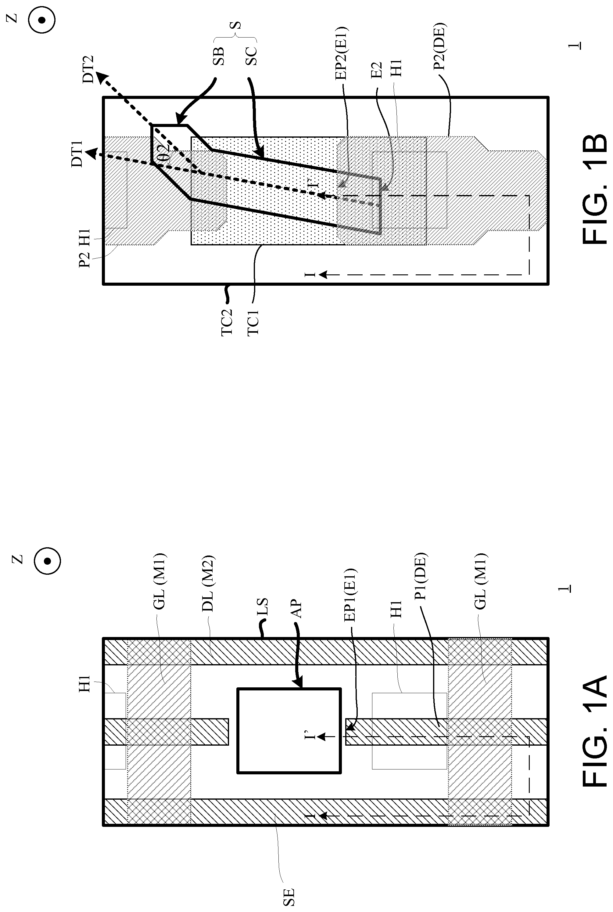
With reference to A to C , A and B respectively illustrate different film layers in the same region of the electronic device to clearly show the relative relationship of how the film layers are disposed. C is a schematic cross-sectional view corresponding to the sectional line I-I′ in A and B . An electronic device 1 may include a substrate SUB 1 , a driving element AD, a first transparent conductive layer TC 1 , an insulating layer PLN, and a second transparent conductive layer TC 2 . The driving element AD is disposed on the substrate SUB 1 and includes a drain electrode DE. The drain electrode DE has a first edge E 1 . The first transparent conductive layer TC 1 is disposed on the driving element AD. The insulating layer PLN is disposed between the driving element AD and the first transparent conductive layer TC 1 and includes a hole H 1 . The first transparent conductive layer TC 1 is electrically connected to the driving element AD through the hole H 1 . The second transparent conductive layer TC 2 is disposed on the insulating layer PLN. One of the first transparent conductive layer TC 1 and the second transparent conductive layer TC 2 includes at least one slit S, and the first transparent conductive layer TC 1 or the second transparent conductive layer TC 2 that includes the at least one slit S has a second edge E 2 . The second edge E 2 is located in the hole H 1 , and the at least one slit S exposes the first edge E 1 of the drain electrode DE. According to some embodiments, the first transparent conductive layer TC 1 may be a pixel electrode, and the second transparent conductive layer TC 2 may be a common electrode. The second edge E 2 of the first transparent conductive layer TC 1 or the second transparent conductive layer TC 2 including the at least one slit S may be an edge of the at least one slit S. For instance, as shown in A to C , the second transparent conductive layer TC 2 includes the slit S, and the second edge E 2 may be the edge of the slit S of the second transparent conductive layer TC 2 .
In detail, the substrate SUB 1 may be a rigid substrate or a flexible substrate. A material of the substrate SUB 1 includes glass, quartz, a ceramic material, sapphire, or a plastic material, which should however not be construed as a limitation in the disclosure. The plastic material includes polycarbonate (PC), polyimide (PI), polypropylene (PP), polyethylene terephthalate (PET), other appropriate flexible materials, or a combination of the aforementioned materials, which should however not be construed as a limitation in the disclosure.
The drain electrode DE of the driving element AD may be a single-layer conductive layer or a multi-layer conductive layer. C is taken as an example. The drain electrode DE is, for instance, a multi-layer conductive layer and includes a first portion P 1 and a second portion P 2 , where the first portion P 1 is located between the second portion P 2 and the substrate SUB 1 , and the second portion P 2 is electrically connected to the first portion P 1 . A material of the first portion P 1 and the second portion P 2 may include metal or a metal stacked layer, such as aluminum, copper, molybdenum, titanium, or a combination thereof, which should however not be construed as a limitation in the disclosure. The second portion P 2 may serve to be adapted to an electrode signal, reduce a contact impedance of the transparent conductive layer (such as the first transparent conductive layer TC 1 ) or block the backlight, and reduce light leakage resulting from the topography of the hole H 1 . In other embodiments, the drain electrode DE of the driving element AD may be a single-layer conductive layer, which is however not shown in the drawings. For instance, the drain electrode DE of the driving element AD in the electronic device 1 may not include the second portion P 2 , which should however not be construed as a limitation in the disclosure.
In addition to the drain electrode DE, the driving element AD may further include a semiconductor pattern CHP, a gate electrode GE, and a source electrode SE, which should however not be construed as a limitation in the disclosure. Thus, the driving element AD may be a thin film transistor (TFT), which should however not be construed as a limitation in the disclosure. The semiconductor pattern CHP is disposed on the substrate SUB 1 . In some embodiments, a material of the semiconductor pattern CHP includes polysilicon, and the semiconductor pattern CHP includes a heavily doped region R 1 , a lightly doped region R 2 , and a channel region R 3 , which should however not be construed as a limitation in the disclosure. C schematically shows three heavily doped regions R 1 , four lightly doped regions R 2 , and two channel regions R 3 , where the lightly doped regions R 2 are located between the heavily doped regions R 1 and the channel regions R 3 . However, it should be understood that design parameters such as the material of the semiconductor pattern CHP, the type or quantity of regions, and so on may be changed according to different requirements and are not limited to those shown in C . For instance, the material of the semiconductor pattern CHP may include amorphous silicon, polysilicon, an oxide semiconductor material, or a combination thereof. The oxide semiconductor is, for instance, indium gallium zinc oxide (IGZO), which should however not be construed as a limitation in the disclosure.
The driving element AD may include the gate electrode GE, and the gate electrode GE may be disposed above or below the semiconductor pattern CHP. For instance, the gate electrode GE overlaps the channel region R 3 in the normal direction Z of the substrate SUB 1 . The normal direction Z of the substrate SUB 1 is, for instance, a direction perpendicular to the upper surface ST of the substrate SUB 1 . A material of the gate electrode GE may include metal or a metal stacked layer, such as aluminum, copper, molybdenum, titanium, or a combination thereof, which should however not be constructed as a limitation in the disclosure. In C , the gate electrode GE is exemplarily disposed above the semiconductor pattern CHP, which should however not be construed as a limitation in the disclosure.
The source electrode SE and the drain electrode DE are disposed above the gate electrode GE, and each of the source electrode SE and the drain electrode DE is electrically connected to the corresponding heavily doped region R 1 through the insulating layer (such as the insulating layer IN 2 and the insulating layer IN 3 ) respectively between the source electrode SE and the semiconductor pattern CHP and between the drain electrode DE and the between semiconductor pattern CHP. A material of the source electrode SE may be referred to as the material of the drain electrode DE, which will not be repeated hereinafter.
It should be understood that C merely schematically illustrates one embodiment of the driving element AD, while the design parameters, such as the type of the driving element AD, the relative relationship of how the electrodes in the driving element AD (such as the gate electrode GE, the source electrode SE, and the drain electrode DE) and/or the semiconductor pattern is disposed, or the number of the electrodes may be changed according to different requirements and should not be limited to those shown in C . According to the top views of A and B , the range indicated by the hole H 1 may represent a bottom or a top of the hole H 1 of the insulating layer PLN in the cross-sectional view of C , e.g., the bottom of the hole H 1 . In this disclosure, the range marked by any hole (such as the hole H 1 or the hole H 2 ) may represent the bottom or the top of the hole of the insulating layer PLN in the corresponding cross-sectional view, e.g., the bottom of the hole.
The insulating layer PLN is disposed on the driving element AD. A material of the insulating layer PLN may include an inorganic material, such as silicon oxide, silicon nitride, silicon oxynitride, aluminum oxide, or an organic material, e.g., perfluoroalkoxy alkane (PFA), which should however not be construed as a limitation in the disclosure.
As shown in the cross-sectional view of C , the hole H 1 of the insulating layer PLN has a sidewall SW. In some embodiments, an included angle θ 1 between the sidewall SW and the upper surface ST of the substrate SUB 1 ranges from 40 degrees to 85 degrees (40 degrees≤θ 1 ≤85 degrees). As shown in the cross-sectional view of the electronic device 1 in C , when the sidewall SW appears to be a straight line, the included angle θ 1 is, for instance, an included angle between an extension line of the sidewall SW and the upper surface ST of the substrate SUB 1 ; when the sidewall SW appears to be a non-linear line (such as an arc), the included angle θ 1 is, for instance, an included angle between a tangent of the sidewall SW at half the height of the sidewall SW and the upper surface ST of the substrate SUB 1 . Given the area observed from the top view stays the same, the greater the included angle θ 1 is, the greater the depth of the hole H 1 is, which is conducive to an increase in the level difference of the same film layer formed on the insulating layer PLN and in the hole H 1 . According to some embodiments, the included angle θ 1 may range from 50 degrees to 85 degrees, e.g., from 65 degrees to 85 degrees or from 70 degrees to 85 degrees.
Given that the drain electrode DE includes the first portion P 1 and the second portion P 2 , the hole H 1 of the insulating layer PLN may partially expose the second portion P 2 , so that the first transparent conductive layer TC 1 may be electrically connected to the second portion P 2 of the drain electrode DE through the hole H 1 , and that the first transparent conductive layer TC 1 is allowed to be electrically connected to the driving element AD. On the other hand, under the framework that the drain electrode DE includes the first portion P 1 but does not include the second portion P 2 , although not shown, the hole H 1 of the insulating layer PLN may partially expose the first portion P 1 , so that the first transparent conductive layer TC 1 may be electrically connected to the first portion P 1 of the drain electrode DE through the hole H 1 , thus allowing the first transparent conductive layer TC 1 to be electrically connected to the driving element AD.
As shown in C , the first transparent conductive layer TC 1 and the second transparent conductive layer TC 2 are disposed on the insulating layer PLN. A material of the first transparent conductive layer TC 1 and the second transparent conductive layer TC 2 may include metal oxide, such as indium tin oxide, aluminum zinc oxide, indium zinc oxide, or other transparent conductive materials, such as graphene or nano-silver, which should however not be construed as a limitation in the disclosure.
In some embodiments, the first transparent conductive layer TC 1 may be located between the second transparent conductive layer TC 2 and the insulating layer PLN (as shown in C ), and the second transparent conductive layer TC 2 may include the at least one slit S (as shown in B or C ). The at least one slit S exposes the first edge E 1 of the drain electrode DE. Under the framework that the drain electrode DE includes the first portion P 1 and the second portion P 2 , the first edge E 1 of the drain electrode DE may include an edge EP 1 of the first portion P 1 and an edge EP 2 of the second portion P 2 , and the at least one slit S may expose the edge EP 1 of the first portion P 1 (as shown in C ) and expose the edge EP 2 of the second portion P 2 (as shown in B ). Under the framework that the drain electrode DE includes the first portion P 1 but does not include the second portion P 2 , the at least one slit S exposes the edge EP 1 of the first portion P 1 . In this embodiment, the first transparent conductive layer TC 1 may be a pixel electrode, the second transparent conductive layer TC 2 may be a common electrode, and the second transparent conductive layer TC 2 is disposed above the first transparent conductive layer TC 1 , thus constituting an electronic device of a top-common type.
In some embodiments, as shown in B , the at least one slit S may include an end portion SB far from the drain electrode DE, and the end portion SB includes a protrusion. In addition, the at least one slit S may further include a trunk portion SC connected to the end portion SB. An included angle θ 2 between an extension direction DT 1 of the trunk portion SC and a direction DT 2 in which the protrusion faces away from the trunk portion SC ranges from 10 degrees to 80 degrees, for instance. For instance, the included angle θ 2 may be 35 degrees, which should however not be construed as a limitation in the disclosure. The extension direction DT 1 of the trunk portion SC refers to an extension direction of a central line of the trunk portion SC, for instance, and the direction DT 2 in which the protrusion faces away from the trunk portion SC is, for instance, the extension direction of the central line of the end portion SB. According to some embodiments, the included angle θ 2 , for instance, ranges from 20 degrees to 70 degrees, e.g., from 25 degrees to 50 degrees or from 30 degrees to 45 degrees.
As shown in B and C , the second transparent conductive layer TC 2 that includes at least one slit S has a second edge E 2 , and the second edge E 2 is located in the hole H 1 . That is, the second edge E 2 overlaps the hole H 1 of the insulating layer PLN in the normal direction Z, and in the cross-sectional view of the electronic device 1 , as shown in C , the second edge E 2 is located between the bottom and the top of the hole H 1 .
In some embodiments, as shown in C , one portion TC 21 of the second transparent conductive layer TC 2 is disposed at the bottom HB of the hole H 1 , and the other portion TC 22 of the second transparent conductive layer TC 2 is disposed on the insulating layer PLN, where the minimum distance D from the portion TC 21 of the second transparent conductive layer TC 2 in the normal direction Z to the other portion TC 22 of the second transparent conductive layer TC 2 ranges from 0.5 μm to 2.5 for instance. In addition, a distance D 1 between the second edge E 2 and the bottom edge of the hole H 1 is, for instance, greater than 0 μm and less than 3 In other embodiments, as shown in C ′, the one portion TC 21 of the second transparent conductive layer TC 2 may be disposed on the sidewall SW of the hole H 1 , which should however not be construed as a limitation in the disclosure. In the normal direction Z, a distance D 2 between the second edge E 2 and the bottom HB of the hole H 1 may range from 0% to 80% of a thickness TH of the insulating layer PLN, e.g., the distance between the bottom of the hole H 1 and the top of the hole H 1 in the normal direction Z.
According to different requirements, as shown in C , the electronic device 1 may further include other film layers or elements. For instance, the electronic device 1 may further include a light shielding pattern LSP, an insulating layer IN 1 , an insulating layer IN 2 , a conductive layer M 1 , an insulating layer IN 3 , a conductive layer M 2 , an insulating layer IN 4 , a conductive layer M 3 , an insulating layer IN 5 , an alignment layer AL 1 , a substrate SUB 2 , a light shielding layer LS, a color filter pattern CF, an insulating layer IN 6 , an alignment layer AL 2 , a spacer PS, and a display medium layer M, which should however not be construed as a limitation in the disclosure. One or a plurality of elements or film layers may be added to or removed from the electronic device 1 according to different demands.
As shown in C , the light shielding pattern LSP is disposed on the substrate SUB 1 and, for instance, overlaps the channel region R 3 in the normal direction Z of the substrate SUB 1 , so as to reduce the interference of the backlight (not shown) of the electronic device 1 in the channel region R 3 . A material of the light shielding pattern LSP may include a light absorbing material or a light reflective material, such as metal or alloy, which should however not be construed as a limitation in the disclosure.
The insulating layer IN 1 is disposed on the substrate SUB 1 and covers the light shielding pattern LSP. A material of the insulating layer IN 1 includes, for instance, an inorganic material, such as silicon oxide, silicon nitride, or silicon oxynitride, which should however not be construed as a limitation in the disclosure.
The semiconductor pattern CHP is disposed on the insulating layer IN 1 and located above the light shielding pattern LSP. The related descriptions of the semiconductor pattern CHP may be referred to as those provided above and thus will not be repeated hereinafter.
The insulating layer IN 2 is disposed on the insulating layer IN 1 and covers the semiconductor pattern CHP. The related descriptions of a material of the insulation layer IN 2 may be referred to as the material of the insulation layer IN 1 provided above and thus will not be repeated hereinafter.
The conductive layer M 1 is disposed on the insulating layer IN 2 and, for instance, includes the gate electrode GE and the scan line GL, which should however not be construed as a limitation in the disclosure. The gate electrode GE is electrically connected to the corresponding scan line GL. The related descriptions of a material of the conductive layer M 1 may be referred to as the material of the gate electrode GE provided above and thus will not be repeated hereinafter.
The insulating layer IN 3 is disposed on the insulating layer IN 2 and covers the conductive layer M 1 . The related descriptions of a material of the insulation layer IN 3 may be referred to as the material of the insulation layer IN 1 provided above and thus will not be repeated hereinafter.
The conductive layer M 2 is disposed on the insulating layer IN 3 and, for instance, includes the first portion P 1 of the drain electrode DE, the source electrode SE, and a data line DL, which should however not be construed as a limitation in the disclosure. The first portion P 1 of the drain electrode DE penetrates the insulating layer IN 3 and the insulating layer IN 2 and is electrically connected to a corresponding heavily doped region R 1 . The source electrode SE is electrically connected to the corresponding data line DL, and the source electrode SE penetrates the insulating layer IN 3 and the insulating layer IN 2 and is electrically connected to another corresponding heavily doped region R 1 . The related descriptions of a material of the conductive layer M 2 may be referred to as the material of the source electrode SE provided above and thus will not be repeated hereinafter.
The insulating layer IN 4 is disposed on the insulating layer IN 3 and covers the conductive layer M 2 . The related descriptions of a material of the insulation layer IN 4 may be referred to as the material of the insulation layer IN 1 provided above and thus will not be repeated hereinafter.
The conductive layer M 3 is disposed on the insulating layer IN 4 and, for instance, includes the second portion P 2 of the drain electrode DE, which should however not be construed as a limitation in the disclosure. The second portion P 2 is disposed above the first portion P 1 , penetrates the insulating layer IN 4 , and is electrically connected to the first portion P 1 . The related descriptions of a material of the conductive layer M 3 may be referred to as the material of the first portion P 1 provided above and thus will not be repeated hereinafter.
The insulating layer PLN is disposed on the insulating layer IN 4 and the conductive layer M 3 , and the hole H 1 of the insulating layer PLN partially exposes the second portion P 2 . The related descriptions of the insulation layer PLN may be referred to as those provided above and thus will not be repeated hereinafter.
The first transparent conductive layer TC 1 is disposed on the insulating layer PLN and extends into the bottom HB of the hole H 1 . The related descriptions of the first transparent conductive layer TC 1 may be referred to as those provided above and thus will not be repeated hereinafter.
The insulating layer IN 5 is disposed on the insulating layer PLN and the first transparent conductive layer TC 1 . The related descriptions of a material of the insulation layer IN 5 may be referred to as the material of the insulation layer IN 1 provided above and thus will not be repeated hereinafter.
The second transparent conductive layer TC 2 is disposed on the insulating layer IN 5 and extends into the hole H 1 . For instance, the second transparent conductive layer TC 2 may extend to the sidewall SW or the bottom HB of the hole H 1 . The related descriptions of the second transparent conductive layer TC 2 may be referred to as those provided above and thus will not be repeated hereinafter.
The alignment layer AL 1 is disposed on the second transparent conductive layer TC 2 and the insulating layer IN 5 , and a portion of the alignment layer AL 1 may cover the second transparent conductive layer TC 2 (e.g., the portion TC 21 ) disposed at the bottom HB of the hole H 1 . A material of the alignment layer AL 1 may include polymers, which should however not be construed as a limitation in the disclosure.
The substrate SUB 2 and the substrate SUB 1 are disposed opposite to each other, and the related descriptions of a material of the substrate SUB 2 may be referred to as the material of the substrate SUB 1 provided above and thus will not be repeated hereinafter.
The light shielding layer LS is disposed on a surface of the substrate SUB 2 facing the substrate SUB 1 and has an aperture AP. The region occupied by the aperture AP is serves as an aperture region of the pixel. The light shielding layer LS may be made of a light absorbing material. The light absorbing material includes black matrix, for instance, which should however not be construed as a limitation in the disclosure.
The color filter pattern CF is disposed in the aperture AP. The electronic device 1 may include a plurality of the color filter patterns CF, such as a plurality of red filter patterns, a plurality of green filter patterns, and a plurality of blue filter patterns, and each of the filter patterns is disposed in a corresponding aperture AP.
The insulating layer IN 6 is disposed on the light shielding layer LS and the color filter pattern CF. The related descriptions of a material of the insulating layer IN 6 may be referred to as the material of the insulation layer IN 1 provided above and thus will not be repeated hereinafter.
The alignment layer AL 2 is disposed on the insulating layer IN 6 . The related descriptions of a material the alignment layer AL 2 may be referred to as the material of the alignment layer AL 1 provided above and thus will not be repeated hereinafter.
The spacer PS may be disposed on the substrate SUB 1 or the substrate SUB 2 , and the display medium layer M may be disposed between the alignment layer AL 1 and the alignment layer AL 2 . C is taken as an example, where the spacer PS is, for instance, disposed on the insulating layer IN 6 on the substrate SUB 2 , and then the alignment layer AL 2 is formed on the insulating layer IN 6 , which should however not be construed as a limitation in the disclosure. In other embodiments not shown in the drawings, the spacer PS may be disposed on the substrate SUB 1 ; for instance, the spacer PS may be disposed on the insulating layer IN 5 on the substrate SUB 1 , and then the alignment layer AL 1 is formed on the insulating layer IN 5 . The spacer PS may serve to keep a liquid crystal cell gap. The electronic device 1 may include a plurality of spacers PS, such as a plurality of main spacers and a plurality of secondary spacers. It should be understood that the main spacers/the secondary spacers are not limited to be formed on the substrate SUB 2 . Although not shown in the drawings, the main spacers/the secondary spacers may be formed on the substrate SUB 1 ; alternately, one of the main spacer and the secondary spacer may be formed on the substrate SUB 2 , and the other of the main spacer and the secondary spacer may be formed on the substrate SUB 1 . A material of the display medium layer M includes liquid crystal, for instance.
Through placing the second edge E 2 of the transparent conductive layer with the at least one slit S (such as the second transparent conductive layer TC 2 ) in the hole H 1 , the hole H 1 of the insulating layer PLN may serve to create the level difference (such as the minimum distance D) of the transparent conductive layer. By the graphic design of the level difference and the slit S, the electric field distribution may be changed, and the ratio of liquid crystal disclination lines entering the aperture region (the top view of the region occupied by the aperture AP) may be reduced, which is conducive to the improvement of the liquid crystal efficiency or the transmissivity. C is taken as an example. Through the above design of the included angle θ 1 and the minimum distance D (that is, the level difference of the second transparent conductive layer TC 2 ), the electric field distribution at the lower left corner of the slit S in the top view of the electronic device 1 (as shown in B ) may be improved, and the liquid crystal efficiency may be further enhanced. In addition, according to the design of the included angle θ 2 , the shape of the end portion SB of the slit S is adjusted, so that the electric field distribution at the upper right corner of the slit S may be improved, and the liquid crystal efficiency may be further enhanced. Under the framework shown in C , the liquid crystal efficiency may be increased to 14%-20% according to a calculation result of a simulation software.
It should be understood that the shape of the end portion SB of the slit S is not limited to what is shown in B . A to E further illustrate various graphic designs of the slit S, but the shape of the slit S in the top views is not limited thereto, and the graphic designs of the slit S shown in A to E may be adopted in any embodiment of the disclosure. According to some embodiments, the end portion SB of the slit S may have an arc shape, as shown in B and C .
In some embodiments, as shown in A , the end portion SB of the slit S may not have the protrusion. In some embodiments, as shown in B to E , the shape of the protrusion of the end portion SB may be different from what is shown in B , and the included angle θ 2 shown in B to E may be different from or the same as what is shown in B . In B to E , the included angle θ 2 is, for instance, 80 degrees, 30 degrees, 50 degrees, and 20 degrees, respectively, but the included angle θ 2 is not limited thereto.
With reference to A to C , A and B respectively illustrate different film layers in the same region of the electronic device to clearly show the relative relationship of how the film layers are disposed. C is a schematic cross-sectional view corresponding to the sectional line I-I′ in A and B . The main differences between an electronic device 1 A and the electronic device 1 shown in A to C are described hereinafter. In the electronic device 1 A, the insulating layer PLN includes a hole H 2 in addition to the hole H 1 . As shown in C , the first transparent conductive layer TC 1 is still disposed at a bottom HB′ of the hole H 2 . The insulating layer IN 5 is further disposed at the bottom HB′ of the hole H 2 and covers the first transparent conductive layer TC 1 disposed at the bottom HB′ of the hole H 2 . The second transparent conductive layer TC 2 further extends into the hole H 2 . For instance, the second transparent conductive layer TC 2 may extend a sidewall SW′ or the bottom HB′ of the hole H 2 . The gate electrode GE on the right side in C and a semiconductor pattern (not shown) may together constitute the driving element AD, so as to be electrically connected to another transparent conductive layer (such as a pixel electrode, not shown). For clear and simple illustration, other related elements are omitted and are not shown in C .
A depth of the hole H 2 is, for instance, less than the depth of the hole H 1 , so as to reduce the possibility of short circuit of the first transparent conductive layer TC 1 disposed at the bottom HB′ of the hole H 2 and the underlying electrode (such as the second portion P 2 of the drain electrode DE). In some embodiments, a halftone mask (HTM) may be applied to form the hole H 1 and the hole H 2 with different depths, thereby reducing the number of times of mask exposures, which should however not be construed as a limitation in the disclosure.
The level difference of the transparent conductive layer (e.g., the level difference of the second transparent conductive layer TC 2 ) is created by forming the hole H 2 of the insulating layer PLN. Since the end portion SB of the slit S is designed to have no protrusion (with reference to B ), the electric field distribution at the upper right corner of the slit S in B may also be improved, which is conducive to a further improvement of the liquid crystal efficiency while the impact of the graphic design of the slit S on the storage capacitor is reduced. Under the framework shown in C , the liquid crystal efficiency may be increased to 22% according to a calculation result of a simulation software.
With reference to A to C , the main differences between an electronic device 1 B and the electronic device 1 shown in A to C are described hereinafter. The electronic device 1 B further includes a bump P. The bump P is, for instance, formed on the insulating layer PLN after the insulating layer PLN is formed, and the bump P covers the sidewall SW of the insulating layer PLN. In some embodiments, as shown in B , the bump P may be disposed corresponding to the upper right corner of the slit S, thereby creating a level difference of the transparent conductive layer (e.g., the level difference of the second transparent conductive layer TC 2 ), so as to improve the electric field distribution at the upper right corner of the slit S in B and further enhance the liquid crystal efficiency. Under the framework shown in C , the liquid crystal efficiency may be increased to 21% according to a calculation result of a simulation software. In other embodiments, although not shown, the bump P may also be disposed corresponding to the lower left corner of the slit S in B , for instance, disposed on the left half of the hole H 1 on the left side in C , thereby improving the level difference of the transparent conductive layer (e.g., the level difference between the portion TC 21 and the portion TC 22 ). Thereby, the electric field distribution at the lower left corner of the slit S in B may be improved, and the liquid crystal efficiency may be further enhanced. Alternately, under the framework shown in C , another bump may be further disposed on the left half of the hole H 1 on the left side in C . The bump P may be an insulating layer and may be made of an organic material, an inorganic material, or a combination thereof, for instance. The material of the bump P may be the same as or different from that of the insulating layer PLN. The bump P may be made of silicon oxide, silicon nitride, silicon oxynitride, or a combination thereof. The gate electrode GE on the right side in C and a semiconductor pattern (not shown) may together constitute the driving element AD, so as to be electrically connected to another transparent conductive layer (such as a pixel electrode, not shown). For clear and simple illustration, other related elements are omitted and are not shown in C .
With reference to A to C , A and B respectively illustrate different film layers in the same region of the electronic device to clearly show the relative relationship of how the film layers are disposed. C is a schematic cross-sectional view corresponding to the sectional line I-I′ in A and B . The main differences between the electronic device 1 C and the electronic device 1 shown in A to C are described hereinafter. In the electronic device 1 C, the second transparent conductive layer TC 2 ′ is located between the first transparent conductive layer TC 1 ′ and the insulating layer PLN, and the first transparent conductive layer TC 1 ′ includes the at least one slit S. The related descriptions of the at least one slit S may be referred to as those provided above and thus will not be repeated hereinafter. In this embodiment, a first transparent conductive layer TC 1 ′ may be a pixel electrode, and a second transparent conductive layer TC 2 ′ may be a common electrode. The first transparent conductive layer TC 1 ′ is disposed above the second transparent conductive layer TC 2 ′ to form an electronic device of a top-pixel type.
The first transparent conductive layer TC 1 ′ including the at least one slit S has a second edge E 2 , and the second edge E 2 is located in the hole H 1 . That is, the second edge E 2 overlaps the hole H 1 in the normal direction Z, and in the cross-sectional view of the electronic device 1 C, as shown in C , the second edge E 2 is located between the bottom and the top of the hole H 1 . In the top view of the electronic device 1 C, as shown in B , the hole H 1 falls within the hole of the second transparent conductive layer TC 2 ′ (shown by a small frame illustrated by thick solid lines in B ), for instance.
In some embodiments, as shown in C , one portion TC 11 of the first transparent conductive layer TC 1 ′ is disposed on the bottom HB of the hole H 1 , and the other portion TC 12 of the first transparent conductive layer TC 1 ′ is disposed on the insulating layer PLN, where the minimum distance D′ between the portion TC 11 of the first transparent conductive layer TC 1 ′ in the normal direction Z and the other portion TC 12 of the first transparent conductive layer TC 1 ′ ranges from 0.5 μm to 2.5 μm, for instance. In addition, a distance D 1 ′ between the second edge E 2 and the bottom edge of the hole H 1 is, for instance, greater than 0 μm and less than 3 μm. In other embodiments, although not shown, the portion TC 11 of the first transparent conductive layer TC 1 ′ may be disposed on the sidewall SW, which should however not be construed as a limitation in the disclosure. In addition, the distance between the second edge E 2 and the bottom HB of the hole H 1 (not shown in C and may be referred to as the distance D 2 shown in C ′) may range from 0% to 80% of the thickness TH of the insulating layer PLN (e.g., the distance from the bottom to the top of the hole H 1 in the normal direction Z).
Through placing the second edge E 2 of the transparent conductive layer with the at least one slit S (such as the first transparent conductive layer TC 1 ′) in the hole H 1 , the hole H 1 of the insulating layer PLN may serve to create the level difference (such as the minimum distance D) of the transparent conductive layer (such as the first transparent conductive layer TC 1 ′). By the graphic design of the level difference and the slit S, the electric field distribution may be changed, and the ratio of liquid crystal disclination lines entering the aperture region (the top view of the region occupied by the aperture AP) may be reduced, which is conducive to the improvement of the liquid crystal efficiency or the transmissivity. C is taken as an example. Through the above design of the included angle θ 1 and the minimum distance D′ (that is, the level difference of the first transparent conductive layer TC 1 ′), the electric field distribution at the lower left corner of the slit S in the top view of the electronic device 1 C (as shown in B ) may be improved, and the liquid crystal efficiency may be further enhanced. In addition, according to the design of the included angle θ 2 , the shape of the end portion SB of the slit S is adjusted, so that the electric field distribution at the upper right corner of the slit S may be improved, and the liquid crystal efficiency may be further enhanced.
To sum up, in one or more embodiments of the disclosure, through placing the second edge of the transparent conductive layer with the at least one slit S (such as the first transparent conductive layer or the second transparent conductive layer) in the hole, the hole of the insulating layer may serve to create the level difference of the transparent conductive layer. By the graphic design of the level difference and the slit, the electric field distribution may be changed, and the ratio of liquid crystal disclination lines entering the aperture region may be reduced, which is conducive to the improvement of the liquid crystal efficiency or the transmissivity.
The above embodiments merely serve to illustrate, but not to limit, the technical solutions of the disclosure. Although the disclosure has been described in detail with reference to the above embodiments, persons skilled in the art should understand that the technical solutions described in the above embodiments can still be modified or some or all of the technical features thereof can be equivalently replaced. However, the modifications or replacements do not cause the essence of the corresponding technical solutions to deviate from the scope of the technical solutions of the embodiments of the disclosure.
Although the embodiments of the disclosure and the advantages thereof have been disclosed above, it should be understood that any person skilled in the art can make changes, substitutions, and modifications without departing from the spirit and scope of the disclosure, and the features of the embodiments can be arbitrarily mixed and replaced to form other new embodiments. In addition, the protection scope of the disclosure is not limited to the process, machine, manufacture, material composition, device, method, and steps in the specific embodiments described in the specification. Any person skilled in the art can understand conventional or future-developed processes, machines, manufactures, material compositions, devices, methods, and steps from the content of the disclosure as long as the same can implement substantially the same functions or achieve substantially the same results in the embodiments described herein. Therefore, the protection scope of the disclosure includes the above processes, machines, manufactures, material compositions, devices, methods, and steps. In addition, each claim constitutes a separate embodiment, and the protection scope of the disclosure further includes combinations of the claims and the embodiments. The protection scope of the disclosure should be defined by the appended claims.
Figures (11)
Citations
This patent cites (1)
- US2022/0328531