Abstract
A flexible display device including a display panel layer, a touch sensing layer, a reflection prevention layer, and a window layer. The touch sensing layer is disposed directly on a first display panel surface, a second display panel surface facing the first display panel surface in a thickness direction, or a second base surface of the reflection prevention layer. The reflection prevention layer is disposed directly on the second display panel surface or a first base surface of the touch sensing layer. The window layer is disposed directly on the first base surface or the second base surface.
Claims (25)
1. A display device, comprising: a base layer; a first organic light emitting element on the base layer; a second organic light emitting element on the base layer; a first black matrix on the first and second organic light emitting elements and having a first transmission opening corresponding to the first organic light emitting element and a second transmission opening corresponding to the second organic light emitting element; a first color filter on the first organic light emitting element and in the first transmission opening; a second color filter on the second organic light emitting element and in the second transmission opening; and a second black matrix on the first and second first color filters and overlapping with the first black matrix, wherein: a portion of the first color filter is disposed on the first black matrix; a portion of the second color filter is disposed on the first black matrix; a first portion of the second black matrix is disposed on the portion of the first color filter and a second portion of the second black matrix is disposed on the portion of the second color filter; the portion of the first color filter is disposed between the first black matrix and the first portion of the second black matrix; and the portion of the second color filter is disposed between the first black matrix and the second portion of the second black matrix.
13. An electronic device, comprising: a display device, wherein the display device comprises: a base layer; a first organic light emitting element on the base layer; a second organic light emitting element on the base layer; a first black matrix on the first and second organic light emitting elements and having a first transmission opening corresponding to the first organic light emitting element and a second transmission opening corresponding to the second organic light emitting element; a first color filter on the first organic light emitting element and in the first transmission opening; a second color filter on the second organic light emitting element and in the second transmission opening; and a second black matrix on the first and second color filters and overlapping with the first black matrix, wherein: a portion of the first color filter is disposed on the first black matrix; a portion of the second color filter is disposed on the first black matrix; a first portion of the second black matrix is disposed on the portion of the first color filter and a second portion of the second black matrix is disposed on the portion of the second color filter; the portion of the first color filter is disposed between the first black matrix and the first portion of the second black matrix; and the portion of the second color filter is disposed between the first black matrix and the second portion of the second black matrix.
Show 23 dependent claims
2. The display device of claim 1 , further comprising a pixel defining layer, wherein: each of the first and second organic light emitting elements comprises a first electrode, an organic light emitting layer on the first electrode, and a second electrode on the organic light emitting layer; and the pixel defining layer has a first opening exposing the first electrode of the first organic light emitting element and a second opening exposing the first electrode of the second organic light emitting element.
3. The display device of claim 2 , wherein: the first opening overlaps with the first transmission opening; and the first opening is disposed inside the first transmission opening on a plane.
4. The display device of claim 1 , further comprising a thin film encapsulation layer encapsulating the first and second organic light emitting elements.
5. The display device of claim 4 , wherein the first black matrix contacts the thin film encapsulation layer.
6. The display device of claim 4 , further comprising a plurality of conductive patterns overlapping with the first black matrix and disposed on the thin film encapsulation layer.
7. The display device of claim 6 , wherein the plurality of conductive patterns contacts the first black matrix or the second black matrix.
8. The display device of claim 1 , wherein the first color filter has a thickness greater than a thickness of the first black matrix.
9. The display device of claim 1 , wherein a boundary between the first color filter and the second color filter overlaps the first black matrix.
10. The display device of claim 1 , further comprising a protection layer including an organic material.
11. The display device of claim 1 , wherein each of the first and second color filters contacts the first black matrix.
12. The display device of claim 11 , wherein the second black matrix contacts each of the first and second color filters.
14. The electronic device of claim 13 , wherein the display device further comprises: each of the first and second organic light emitting elements comprises a first electrode, an organic light emitting layer on the first electrode, and a second electrode on the organic light emitting layer; and the pixel defining layer has a first opening exposing the first electrode of the first organic light emitting element and a second opening exposing the first electrode of the second organic light emitting element.
15. The electronic device of claim 14 , wherein: the first opening overlaps with the first transmission opening; and the first opening is disposed inside the first transmission opening on a plane.
16. The electronic device of claim 13 , wherein the display device further comprises a thin film encapsulation layer encapsulating the first and second organic light emitting elements.
17. The electronic device of claim 16 , wherein the first black matrix contacts the thin film encapsulation layer.
18. The electronic device of claim 16 , wherein the display device further comprises a plurality of conductive patterns overlapping with the first black matrix and disposed on the thin film encapsulation layer.
19. The electronic device of claim 18 , wherein the plurality of conductive patterns contacts the first black matrix or the second black matrix.
20. The electronic device of claim 13 , wherein the first color filter has a thickness greater than a thickness of the first black matrix.
21. The electronic device of claim 13 , wherein a boundary between the first color filter and the second color filter overlaps the first black matrix.
22. The electronic device of claim 13 , wherein the display device further comprises a protection layer including an organic material.
23. The electronic device of claim 13 , wherein each of the first and second color filters contacts the first black matrix.
24. The electronic device of claim 23 , wherein the second black matrix contacts each of the first and second color filters.
25. The electronic device of claim 13 , wherein the electronic device is one of a television, a monitor, a mobile phone, a tablet, a notebook, a personal computer, a navigation unit for vehicle, a game console, and a smart watch.
Full Description
Show full text →
CROSS-REFERENCE TO RELATED APPLICATIONS
This application is a Continuation of U.S. patent application Ser. No. 17/676,730, filed Feb. 21, 2022, which is a Continuation of U.S. patent application Ser. No. 16/698,634, filed Nov. 27, 2019, which issued as U.S. Pat. No. 11,257,875, which is a Division of U.S. patent application Ser. No. 15/285,270, filed Oct. 4, 2016, which issued as U.S. Pat. No. 10,504,971, and claims priority to and the benefit of Korean Patent Application No. 10-2016-0036369, filed Mar. 25, 2016, each of which is hereby incorporated by reference for all purposes as if fully set forth herein.
BACKGROUND
Field
Exemplary embodiments relate to a flexible display device, and, more particularly, to a flexible display device including integrated functional members.
Discussion of the Background
Electronic devices, such as smartphones, digital cameras, laptop computers, tablets, navigational aids, televisions, and the like, may permit users to intentionally deform the device in various manners and shapes. In this manner, a display device (e.g., a flat panel display device) of an electronic device may also be deformed in correspondence with the deformation of the electronic device. As such, flexible display devices, such as curved display devices, bent display devices, rolled display devices, and the like, are of interest.
The above information disclosed in this Background section is only for enhancement of understanding of the background of the inventive concept, and, therefore, it may contain information that does not form the prior art that is already known to a person of ordinary skill in the art.
SUMMARY
One or more exemplary embodiments provide a flexible display device having improved flexibility.
Additional aspects will be set forth in the detailed description which follows, and, in part, will be apparent from the disclosure, or may be learned by practice of the inventive concept.
According to one or more exemplary embodiments, a flexible display device includes a display panel layer, a touch sensing layer, a reflection prevention layer, and a window layer. The display panel layer includes a display area and a non-display area. The display area includes a plurality of light emitting areas and a non-light emitting area adjacent to the plurality of light emitting areas. The non-display area is disposed adjacent to the display area. The display panel layer forms a first display panel surface and a second display panel surface facing the first display panel surface in a thickness direction. The touch sensing layer forms a first base surface. The reflection prevention layer forms a second base surface. The window layer forms an outer surface. The touch sensing layer is disposed directly on one of the first display panel surface, the second display panel surface, and the second base surface. The reflection prevention layer is disposed directly on the second display panel surface or the first base surface. The window layer is disposed directly on the first base surface or the second base surface.
According to one or more exemplary embodiments, a flexible display device includes a display panel layer, a touch sensing layer, and a window layer. The display panel layer includes a display area and a non-display area. The display area includes a plurality of light emitting areas and a non-light emitting area adjacent to the plurality of light emitting areas. The non-display area is disposed adjacent to the display area. The display panel layer forms a first display panel surface and a second display panel surface facing the first display panel surface in a thickness direction. The touch sensing layer forms a first base surface. The window layer forms an outer surface. The touch sensing layer is disposed directly on the second display panel surface. The window layer is disposed directly on the first base surface. The touch sensing layer includes: a plurality of first conductive patterns overlapping with the non-light emitting area, the plurality of first conductive patterns being disposed directly on the second display panel surface; a plurality of second conductive patterns overlapping with the non-light emitting area; and a touch insulation layer configured to insulate the first conductive patterns from the second conductive patterns. The touch insulation layer includes: a black matrix overlapping with the non-light emitting area and the non-display area, and a plurality of color filters respectively overlapping with the plurality of light emitting areas.
According to one or more exemplary embodiments, a flexible display device includes a display panel layer, a touch sensing layer, and a window layer. The display panel layer includes a display area and a non-display area. The display area includes a plurality of light emitting areas and a non-light emitting area adjacent to the plurality of light emitting areas. The non-display area is adjacent to the display area, the display panel layer forming a first display panel surface and a second display panel surface facing the first display panel surface in a thickness direction. The touch sensing layer forms a first base surface. The window layer forms an outer surface. The touch sensing layer is disposed directly on the second display panel surface. The window layer is disposed directly on the first base surface. The display panel layer further includes: a first metal layer; a transparent conductive layer disposed directly on the first metal layer; and a second metal layer disposed directly on the transparent conductive layer.
According to one or more exemplary embodiments, a flexible display device includes a display panel layer, a touch sensing layer, a black matrix, and a window layer. The display panel layer includes a display area and a non-display area. The display area includes a plurality of light emitting areas and a non-light emitting area adjacent to the plurality of light emitting areas. The non-display area is adjacent to the display area, the display panel layer forming a first display panel surface and a second display panel surface facing the first display panel surface in a thickness direction. The touch sensing layer forms a first base surface. The black matrix overlaps with the non-light emitting area and the non-display area. The window layer forms an outer surface. The touch sensing layer is disposed directly on one of the first display panel surface and the second display panel surface. The black matrix is disposed directly on the second display panel surface or the first base surface. The window layer is disposed directly on and covers the black matrix.
According to one or more exemplary embodiments, a method of manufacturing a flexible display device includes: forming a display panel layer configured to display an image; forming a touch sensing layer directly contacting the display panel layer, the touch sensing layer being configured to sense touch interactions associated with the image; forming a reflection prevention layer directly contacting the display panel layer or the touch sensing layer, the reflection prevention layer being configured to reduce external light reflection from the display panel layer; and forming a window layer directly contacting the reflection prevention layer.
According to one or more exemplary embodiments, a method of manufacturing a flexible display device includes: forming one or more first layers configured to generate an image on a first outermost layer of the one or more first layers; and forming one or more second layers configured to reduce external light reflection off the one or more first layers. The one or more second layers include: a second outermost layer directly contacting the first outermost layer; and a third outermost layer opposing the second outermost layer. The method further includes forming one or more third layers configured to sense touch interactions in association with the image. The one or more third layers include: a fourth outermost layer directly contacting the third outermost layer; and a fifth outermost layer opposing the fourth outermost layer. The method further includes forming one or more fourth layers configured to at least protect the one or more first layers, the one or more fourth layers comprising a sixth outermost layer directly contacting the fifth outermost layer.
According to one or more exemplary embodiments, a method of manufacturing a flexible display device includes forming a display panel layer configured to generate an image in a display area. The display area includes: a plurality of light emitting areas; and a plurality of non-light emitting areas. The method further includes forming, directly on the display panel layer, a touch sensing layer configured to: sense touch interactions associated with the image; and reduce a reflective index of external light. The method further includes forming, directly on the touch sensing layer, a window layer. The touch sensing layer includes: a plurality of conductive patterns configured to sense the touch interactions, the plurality of conductive patterns being formed directly on the display panel layer and overlapping with the plurality of non-light emitting areas; a touch insulation layer covering the plurality of first conductive patterns, the touch insulation layer including a plurality of openings overlapping with the plurality of light emitting areas; and a plurality of color filters formed directly on the display panel layer in the plurality of openings, the plurality of color filters being configured to reduce the reflective index of the external light.
According to one or more exemplary embodiments, a method of manufacturing a flexible display device includes forming a display panel layer including: an encapsulation layer; a light emitting layer configured to emit light onto a surface of the encapsulation layer; and electrodes configured to drive the light emitting layer. The method further includes: forming a touch sensing layer directly on the surface of the encapsulation layer; and forming a window layer directly on a surface of the touch sensing layer. At least one of the electrodes includes: a first metal layer; a transparent conductive layer disposed directly on the first metal layer; and a second metal layer disposed directly on the transparent conductive layer.
The foregoing general description and the following detailed description are exemplary and explanatory and are intended to provide further explanation of the claimed subject matter.
BRIEF DESCRIPTION OF THE DRAWINGS
The accompanying drawings, which are included to provide a further understanding of the inventive concept, and are incorporated in and constitute a part of this specification, illustrate exemplary embodiments of the inventive concept, and, together with the description, serve to explain principles of the inventive concept.
A is a perspective view of illustrating a first operational state of a flexible display device, according to one or more exemplary embodiments.
B is a perspective view illustrating a second operational state of the flexible display device of A , according to one or more exemplary embodiments.
C is a perspective view illustrating a third operational state of the flexible display device of A , according to one or more exemplary embodiments.
A is a cross-sectional view of the flexible display device of A in the first operational state, according to one or more exemplary embodiments.
B is a cross-sectional view of the flexible display device of B in the second operational state, according to one or more exemplary embodiments.
C is a cross-sectional view of the flexible display device of C in the third operational state, according to one or more exemplary embodiments.
A is a cross-sectional view of a flexible display device in a second operational state, according to one or more exemplary embodiments.
B is a cross-sectional view of the flexible display device of A in a third operational state, according to one or more exemplary embodiments.
A, 4 B, 4 C, and 4 D are cross-sectional views of flexible display devices in first operational states, according to one or more exemplary embodiments.
is a perspective view of a flexible display panel, according to one or more exemplary embodiments.
is an equivalent circuit diagram of a pixel of the flexible display panel of , according to one or more exemplary embodiments.
is a partial plan view of an organic light emitting display panel, according to one or more exemplary embodiments.
A and 8 B are partial cross-sectional views of the organic light emitting display panel of , according to one or more exemplary embodiments.
A, 9 B, and 9 C are cross-sectional views of thin film encapsulation layers, according to one or more exemplary embodiments.
A, 10 B, and 10 C are cross-sectional views of display devices, according to one or more exemplary embodiments.
A and 11 B are plan views illustrating conductive layers of a touch detection member, according to one or more exemplary embodiments.
A is a partial enlarged view of area AA in A , according to one or more exemplary embodiments.
B and 12 C are a partial cross-sectional views of A respectively taken along sectional lines I-I′ and according to one or more exemplary embodiments.
A is a partial enlarged view of area BB in B , according to one or more exemplary embodiments.
B and 13 C are partial cross-sectional views of A respectively taken along sectional lines and IV-IV′, according to one or more exemplary embodiments.
A is a partial enlarged view of area CC in B , according to one or more exemplary embodiments.
B is a partial cross-sectional view of A taken along sectional line V-V′, according to one or more exemplary embodiments.
A and 15 B are plan views illustrating conductive layers of a touch detection member, according to one or more exemplary embodiments.
C is a partial enlarged view of area CC in B , according to one or more exemplary embodiments.
D is a partial cross-sectional view of C taken along sectional line VI-VI′, according to one or more exemplary embodiments.
A, 16 B, and 16 C are partial cross-sectional views of display devices, according to one or more exemplary embodiments.
A, 17 B, 17 C, 17 D, and 17 E are cross-sectional views of display devices, according to one or more exemplary embodiments.
A, 18 B, 18 C, and 18 D are cross-sectional views of display devices, according to one or more exemplary embodiments.
A, 19 B, 19 C, 19 D, 19 E, and 19 F are cross-sectional views of display devices, according to one or more exemplary embodiments.
A and 20 B are cross-sectional views of a display device, according to one or more exemplary embodiments.
A and 21 B are cross-sectional views of cathodes of organic light emitting diodes of display devices, according to one or more exemplary embodiments.
DETAILED DESCRIPTION OF THE ILLUSTRATED EMBODIMENTS
In the following description, for the purposes of explanation, numerous specific details are set forth in order to provide a thorough understanding of various exemplary embodiments. It is apparent, however, that various exemplary embodiments may be practiced without these specific details or with one or more equivalent arrangements. In other instances, well-known structures and devices are shown in block diagram form in order to avoid unnecessarily obscuring various exemplary embodiments.
Unless otherwise specified, the illustrated exemplary embodiments are to be understood as providing exemplary features of varying detail of various exemplary embodiments. Therefore, unless otherwise specified, the features, components, modules, layers, films, panels, regions, and/or aspects of the various illustrations may be otherwise combined, separated, interchanged, and/or rearranged without departing from the disclosed exemplary embodiments. Further, in the accompanying figures, the size and relative sizes of layers, films, panels, regions, etc., may be exaggerated for clarity and descriptive purposes. When an exemplary embodiment may be implemented differently, a specific process order may be performed differently from the described order. For example, two consecutively described processes may be performed substantially at the same time or performed in an order opposite to the described order. Also, like reference numerals denote like elements.
When an element or layer is referred to as being “on,” “connected to,” or “coupled to” another element or layer, it may be directly on, connected to, or coupled to the other element or layer or intervening elements or layers may be present. When, however, an element or layer is referred to as being “directly on,” “directly connected to,” or “directly coupled to” another element or layer, there are no intervening elements or layers present. Further, the DR 1 -axis, the DR 2 -axis, and the DR 3 -axis are not limited to three axes of a rectangular coordinate system, and may be interpreted in a broader sense. For example, the DR 1 -axis, the DR 2 -axis, and the DR 3 -axis may be perpendicular to one another, or may represent different directions that are not perpendicular to one another. For the purposes of this disclosure, “at least one of X, Y, and Z” and “at least one selected from the group consisting of X, Y, and Z” may be construed as X only, Y only, Z only, or any combination of two or more of X, Y, and Z, such as, for instance, XYZ, XYY, YZ, and ZZ. As used herein, the term “and/or” includes any and all combinations of one or more of the associated listed items.
Although the terms “first,” “second,” etc. may be used herein to describe various elements, components, regions, layers, and/or sections, these elements, components, regions, layers, and/or sections should not be limited by these terms. These terms are used to distinguish one element, component, region, layer, and/or section from another element, component, region, layer, and/or section. Thus, a first element, component, region, layer, and/or section discussed below could be termed a second element, component, region, layer, and/or section without departing from the teachings of the present disclosure.
Spatially relative terms, such as “beneath,” “below,” “lower,” “above,” “upper,” and the like, may be used herein for descriptive purposes, and, thereby, to describe one element or feature′s relationship to another element(s) or feature(s) as illustrated in the drawings. Spatially relative terms are intended to encompass different orientations of an apparatus in use, operation, and/or manufacture in addition to the orientation depicted in the drawings. For example, if the apparatus in the drawings is turned over, elements described as “below” or “beneath” other elements or features would then be oriented “above” the other elements or features. Thus, the exemplary term “below” can encompass both an orientation of above and below. Furthermore, the apparatus may be otherwise oriented (e.g., rotated 90 degrees or at other orientations), and, as such, the spatially relative descriptors used herein interpreted accordingly.
The terminology used herein is for the purpose of describing particular embodiments and is not intended to be limiting. As used herein, the singular forms, “a,” “an,” and “the” are intended to include the plural forms as well, unless the context clearly indicates otherwise. Moreover, the terms “comprises,” “comprising,” “includes,” and/or “including,” when used in this specification, specify the presence of stated features, integers, steps, operations, elements, components, and/or groups thereof, but do not preclude the presence or addition of one or more other features, integers, steps, operations, elements, components, and/or groups thereof.
Various exemplary embodiments are described herein with reference to sectional illustrations that are schematic illustrations of idealized exemplary embodiments and/or intermediate structures. As such, variations from the shapes of the illustrations as a result, for example, of manufacturing techniques and/or tolerances, are to be expected. Thus, exemplary embodiments disclosed herein should not be construed as limited to the particular illustrated shapes of regions, but are to include deviations in shapes that result from, for instance, manufacturing. For example, an implanted region illustrated as a rectangle will, typically, have rounded or curved features and/or a gradient of implant concentration at its edges rather than a binary change from implanted to non-implanted region. Likewise, a buried region formed by implantation may result in some implantation in the region between the buried region and the surface through which the implantation takes place. Thus, the regions illustrated in the drawings are schematic in nature and their shapes are not intended to illustrate the actual shape of a region of a device and are not intended to be limiting.
Unless otherwise defined, all terms (including technical and scientific terms) used herein have the same meaning as commonly understood by one of ordinary skill in the art to which this disclosure is a part. Terms, such as those defined in commonly used dictionaries, should be interpreted as having a meaning that is consistent with their meaning in the context of the relevant art and will not be interpreted in an idealized or overly formal sense, unless expressly so defined herein.
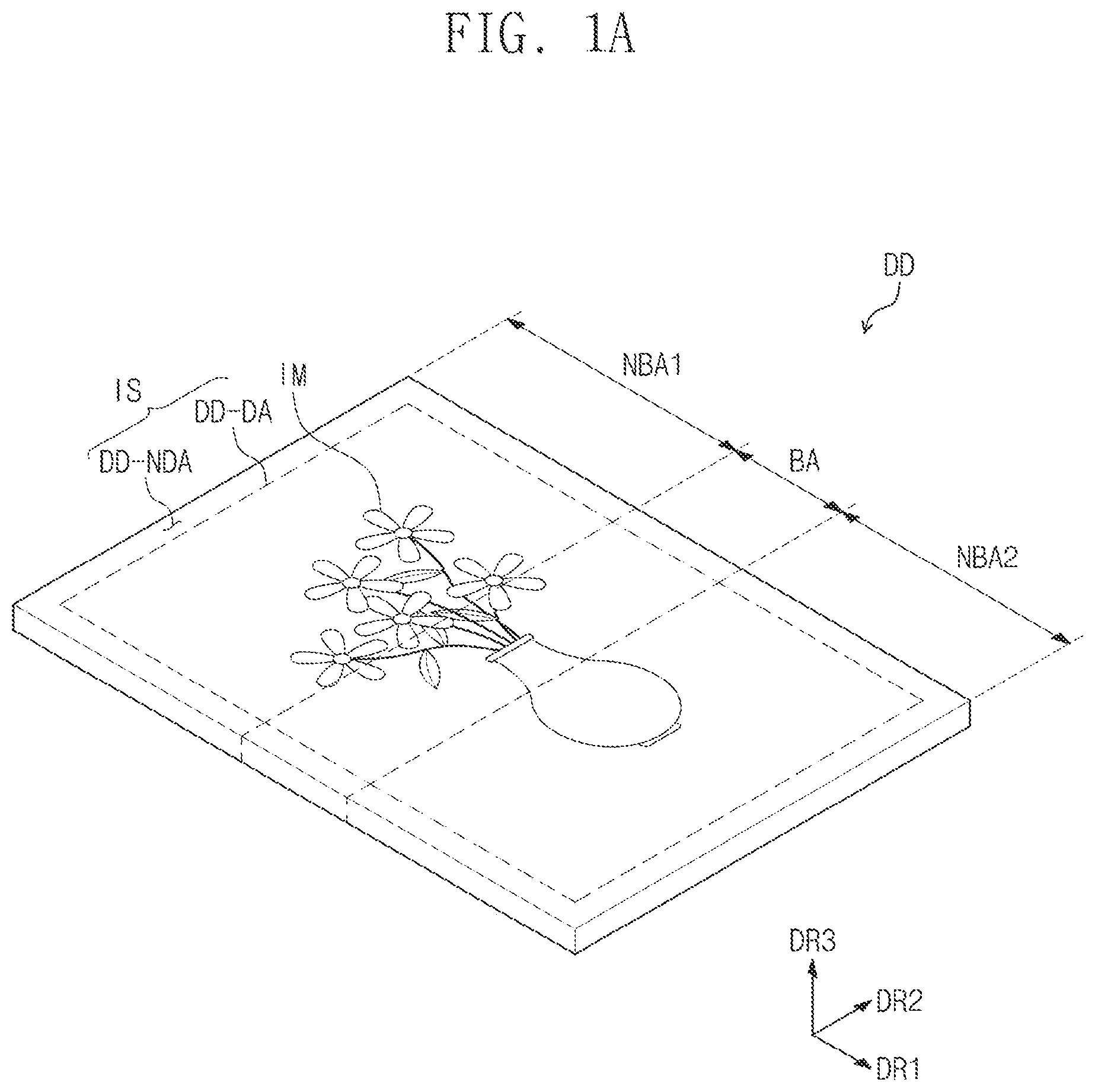
A, 1 B, and 1 C are perspective views respectively illustrating first, second, and third operational states of a flexible display device DD, according to one or more exemplary embodiments. A, 2 B, and 2 C are cross-sectional views respectively illustrating the first, second, and third operational states of the flexible display device DD, according to one or more exemplary embodiments.
A display surface IS on which an image IM is displayed is parallel to a surface defined by a first directional axis DR 1 and a second directional axis DR 2 . A normal direction of the display surface IS, i.e., a thickness direction of the flexible display device DD, is indicated as a third directional axis DR 3 . A front surface (or a top surface) and a rear surface (or a bottom surface) of each of the members (or components) of the flexible display device DD are distinguished from one another in the third directional axis DR 3 . Directions indicated in association with the first to third directional axes DR 1 , DR 2 , and DR 3 are merely relative, and, as such, may be changed to different directions with respect to each other. Hereinafter, the first to third directions may be expressed by the same reference symbols as the directions indicated in association with the first to third directional axis DR 1 , DR 2 , and DR 3 , respectively.
A foldable display device is illustrated as an example of the flexible display device DD of A to 1 C and 2 A to 2 C . It is contemplated, however, that exemplary embodiments are not limited thereto or thereby. For instance, the flexible display device DD may be provided as a rollable display device that may be wound. It is noted that the flexible display device DD may be used for large-scale electronic apparatuses, such as televisions, monitors, etc., and middle and small-scale electrode apparatuses, such as mobile phones, tablets, notebooks, personal computers, navigation units for vehicles, game consoles, smart watches, etc.
As illustrated in A , the display surface IS of the flexible display device DD may be divided into a plurality of areas. The flexible display device DD may include a display area DD-DA on which the image IM is displayed (or perceived), and a non-display area DD-NDA that is disposed adjacent to (or outside of) the display area DD-DA. The non-display area DD-NDA may be an area on which the image IM is not displayed. A flower vase is illustrated as an example of the image IM in A . For example, the display area DD-DA may have a rectangular shape, and the non-display area DD-NDA may surround the display area DD-DA. It is contemplated, however, that exemplary embodiments are not limited thereto or thereby. For example, the shape of the display area DD-DA and the shape of the non-display area DD-NDA may be relatively designed with respect to each other. To this end, the respective shapes of the display area DD-DA and the non-display area DD-NDA may be the same as one another or different from one another.
As seen in A to 1 C , the flexible display device DD may include a bending area BA that is bendable with respect to a bending axis BX, and first and second non-bending areas NBA 1 and NBA 2 that are not bendable. As illustrated in B , the flexible display device DD may be bent inward so that the display surface IS of the first non-bending area NDA 1 and the display surface IS of the second non-bending area NBA 2 face each other. As illustrated in C , the flexible display device DD may be bent outward to expose the display surface IS to the outside.
According to one or more exemplary embodiments, the flexible display device DD may include a plurality of bending areas BA. In addition, the bending areas BA may be defined to correspond to a configuration of the flexible display device DD that is manipulated by a user, e.g., the bending areas may be dynamically configured by the user. For example, the bending area BA may be defined in parallel to the first directional axis DR 1 or defined in a diagonal direction, unlike as shown in B and 1 C . In one or more exemplary embodiments, the flexible display device DD may be configured to only repeat the operational modes of A to 1 C .
As illustrated in A to 2 C , the flexible display device DD includes an external protection member PL, a display panel member DP, a touch detection member TS, a reflection prevention member RPL, and a window member WL. The external protection member PL, the display panel member DP, the touch detection member TS, the reflection prevention member RPL, and the window member WL may be integrally formed through a continuous process to form an external protection layer PL, a display panel layer DP, a touch sensing layer TS, a reflection prevention layer RPL, and a window layer WL of the flexible display device DD. Hereinafter, the external protection member PL, the display panel member DP, the touch detection member TS, the reflection prevention member RPL, and the window member WL of the flexible display device DD may be referred to as the external protection layer PL, the display panel layer DP, the touch sensing layer TS, the reflection prevention layer RPL, and the window layer WL, respectively.
Although the flexible display device DD including the functional layers that are successively stacked from the external protection layer PL to the window layer WL is illustrated as an example exemplary embodiments are not limited thereto or thereby. For instance, the stacked order of the functional layers may be changed. In addition, portions of the functional layers may be omitted, or two functional layers may be replaced with one functional layer.
The display panel layer DP generates the image (see reference symbol IM of A ) corresponding to input image data. The display panel layer DP provides a first display panel surface BS 1 -L (or a base bottom surface) and a second display panel surface BS 1 -U (or a base top surface), which face each other in the thickness direction DR 3 . The display panel layer DP may be an organic light emitting display panel, an electrophoretic display panel, or an electrowetting display panel. It is contemplated, however, that exemplary embodiments are not limited to a kind (or type) of display panel, and, as such, any suitable display panel may be utilized in association with exemplary embodiments described herein. For descriptive and illustrative convenience, exemplary embodiments will be described in association with an organic light emitting display panel embodiment. The organic light emitting display panel will be described later in more detail.
The external protection layer PL is disposed on (e.g., directly on) the first display panel surface BS 1 -L to protect the display panel layer DP. The external protection layer PL provides a first outer surface OS-L of the flexible display device DD. The external protection layer PL prevents external moisture, oxygen, debris, etc., from permeating into the display panel layer DP. The external protection layer PL may also function to absorb external impacts. The external protection layer PL may be formed of a plastic resin. The external protection layer PL may be formed of a material selected from the group consisting of polyethersulphone (PES), polyacrylate (PAR), polyetherimide (PEI), polyethylene naphthalate (PEN), polyethylene terepthalate (PET), polyphenylene sulfide (PPS), polyallylate, polyimide (PI), polycarbonate (PC), poly(arylene ether sulfone), and a combination thereof.
According to one or more exemplary embodiments, the material forming the external protection layer PL is not limited to plastic resins. For example, the external protection layer PL may be formed of an organic/inorganic composite material. The external protection layer PL may include a porous organic layer and an inorganic material filled into pores of the organic layer. It is also noted that the external protection layer PL may be formed on the first display panel surface BS 1 -L in a coating or printing manner. For instance, the external protection layer PL may be formed by using roll coating, silkscreen costing, spray coating, slit coating, and/or the like. The external protection layer PL may be omitted according to a configuration of the display panel layer DP.
The touch sensing layer TS acquires coordinate information of an external input, e.g., user input. The touch sensing layer TS may be disposed on (e.g., directly on) the second display panel surface BS 1 -U. The touch sensing layer TS provides a first base surface BS 2 (or a touch base surface). It is contemplated that the touch sensing layer TS may be manufactured together with the display panel layer DP via a continuous process. For illustrative and descriptive convenience, the touch sensing layer TS will be described in association with a capacitive touch detection member embodiment. Exemplary embodiments, however, are not limited thereto or thereby. For example, the touch sensing layer TS may be replaced with another touch sensing layer including two types of touch electrodes, such as an electromagnetic induction touch detection member. A capacitive touch sensing layer will be described later in more detail.
The reflection prevention layer RPL may absorb light incident from the outside or destructively interfere with the light to reduce external light reflectance of the flexible display device DD. The reflection prevention layer RPL may be disposed on (e.g., directly on) the first base surface BS 2 . The reflection prevention layer RPL provides a second base surface BS 3 (or a reflection prevention base surface). In one or more exemplary embodiments, the reflection prevention layer RPL may be manufactured together with the touch sensing layer TS via a continuous process. In this manner, the reflection prevention layer RPL may constitute a portion of the touch sensing layer TS or a portion of the display panel layer DP. The reflection prevention layer RPL will be described later in more detail.
The window layer WL may be disposed on (e.g., directly on) the second base surface BS 3 to protect the display panel layer DP. The window layer WL provides a second outer surface OS-U of the flexible display device DD. The display surface IS of A to 1 C may be the second outer surface OS-U. In one or more exemplary embodiments, the window layer WL may be manufactured together with the reflection prevention layer RPL via a continuous process. The window layer WL will be described later in more detail.
Although not separately shown, the flexible display device DD may further include a frame structure supporting the functional layers to maintain the operational states illustrated in A to 2 C . The frame structure may include a joint structure or a hinge structure.
As illustrated in B , the flexible display device DD may be bent inward at a determined radius of curvature BR by, for instance, user manipulation. Alternatively, as illustrated in C , the flexible display device DD may be bent outward at a determined radius of curvature BR by, for example, user manipulation. It is also contemplated that the flexible display device DD may be bidirectionally bent according to user manipulation. The bidirectional bending may be repeatedly performed. The radius of curvature BR may be constantly maintained. The first non-bending area NBA 1 and the second non-bending area NBA 2 may face each other and may be extend parallel to one another. The bending area BA may not be fixed in surface area, but be determined according to the radius of curvature BR. The user may perceive an image from the flexible display device DD in the non-bent state of A .
The touch sensing layer TS, the reflection prevention layer RPL, the window layer WL, and the external protection layer PL may be integrated with the display panel DP through a continuous process, and, as such, separate adhesion members conventionally formed between one or more of the touch sensing layer TS, the reflection prevention layer RPL, the window layer WL, the external protection layer PL, and the display panel DP may be omitted. Since the various adhesion members may be omitted, the flexible display device DD may be reduced in thickness and improved in flexibility. The flexible display device DD may have the total thickness less than about 100 micrometers. An adhesion member, such as an optically clear adhesive (OCA), may have a thickness greater than about 20 micrometers. By omitting one or more adhesion members the thickness of the flexible display device DD may be reduced.
A and 3 B are cross-sectional views of a flexible display device in second and third operational states, according to one or more exemplary embodiments. A to 4 D are cross-sectional views flexible display devices in first operational states, according to one or more exemplary embodiments. The flexible display devices of A, 3 B, and 4 A to 4 D are similar to the flexible display device DD of A to 1 C and 2 A to 2 C , and, as such, duplicative descriptions have been omitted to avoid obscuring exemplary embodiments described herein. In this manner, differences are primarily described below.
The flexible display device DD′ may be bidirectionally bent in the shape illustrated in A and 3 B . The bending area BA′ may be bent in a shape that is more similar to a circular shape to increase a surface area of the bending area BA′ when compared to that of the being area BA of the flexible display device DD of A to 1 C and 2 A to 2 C . Also, the bending area BA′ may be bent at a radius of curvature BR′ greater than the radius of curvature BR illustrated in B and 2 C to reduce stress of the bending area BA.
As illustrated in A and 4 B , functional layers may be changed in stacking order. For instance, in A , a touch sensing layer TS may be disposed on a first display panel surface BS 1 -L. An external protection layer PL may be disposed on a first base surface BS 2 . A reflection prevention layer RPL may be disposed on a second display panel surface BS 1 -U. A window layer WL may be disposed on a second base surface BS 3 . In B , the reflection prevention layer RPL may be disposed on the second display panel surface BS 1 -U. The touch sensing layer TS may be disposed on the second base surface BS 3 . The window layer WL may be disposed on the first base surface BS 2 .
As illustrated in C and 4 D , the reflection prevention layer RPL that is separately formed in the other flexible display devices may be combined with another functional layer. The reflection prevention layer may constitute a portion of the touch sensing layer TS or a portion of a display panel layer DP. For example, in C , a touch sensing layer TS-R may have also have the function of the reflection prevention layer RPL. The touch sensing layer TS-R may be disposed on the second display panel surface BS 1 -U, and the window layer WL may be disposed on the base surface BS 2 . In D , a display panel layer DP-R may also have the function of the reflection prevention layer RPL. The touch sensing layer TS may be disposed on the hybrid second display panel surface BS 1 -R-U, and the window layer WL may be disposed on the first base surface BS 2 . The external protection layer PL may be disposed on the hybrid first display panel surface BS 1 -R-L.
is a perspective view of a flexible display panel, according to one or more exemplary embodiments. is an equivalent circuit diagram of a pixel of the flexible display panel of , according to one or more exemplary embodiments.
Hereinafter, the flexible display panel layer DP will be described as an organic light emitting display panel layer DP. The organic light emitting display panel layer DP includes a display area DA and a non-display area NDA on a plane. The second display panel surface BS 1 -U may be divided into the display area DA and the non-display area NDA. The display area DA and the non-display area NDA of the second display panel surface BS 1 -U do not need to match the display area DD-DA and the non-display area DD-NDA of the flexible display device DD. For example, the display area DA and the non-display area NDA of the second display panel surface BS 1 -U may be configured according a structure and/or design of the organic light emitting display panel layer DP.
As illustrated in , the organic light emitting display panel layer DP includes a plurality of pixels PX disposed on the display area DA. Although the plurality of pixels PX are shown as being arranged in a matrix shape, exemplary embodiments are not limited thereto or thereby. The plurality of pixels PX may be arranged in any suitable shape, such as a non-matrix shape, e.g., a pantile shape.
illustrates an example of an equivalent circuit of a representative pixel PXij to which an i-th scan line SLi and a j-th source line DLj are connected. Although not separately shown, the plurality of pixels PX may have the same equivalent circuit as representative pixel PXij. The pixel PXij includes at least two transistors TR 1 and TR 2 , at least one capacitor CAP, and an organic light emitting device OLED. Although a pixel driving circuit including two transistors TR 1 and TR 2 and one capacitor CAP is illustrated as an example, exemplary embodiments are not limited to the configuration of the pixel driving circuit.
An anode of the organic light emitting device OLED receives a first power voltage ELVDD applied to a power line PWL through the second transistor TR 2 . A cathode of the organic light emitting device OLED receives a second power voltage ELVSS. The first transistor TR 1 outputs a data signal applied to a j-th source line DLj in response to a scanning signal applied to the i-th scan line SLi. The capacitor CAP charges a voltage to correspond to the data signal received from the first transistor TR 1 . The second transistor TR 2 controls driving current flowing through the organic light emitting device OLED to correspond to a voltage stored in the capacitor CAP.
is a partial plan view of a portion of the organic light emitting display panel of , according to one or more exemplary embodiments. A and 8 B are partial cross-sectional views of the organic light emitting display panel of , according to one or more exemplary embodiments.
corresponds to a portion DP-P of the organic light emitting display panel of . A is a partial cross-sectional view of a portion corresponding to the first transistor TR 1 and the capacitor CAP of the equivalent circuit of , whereas B is a partial cross-sectional view of a portion corresponding to the second transistor TR 2 and the organic light emitting device OLED of the equivalent circuit of . In A and 8 B , an external protection layer PL disposed on a first outer surface OS-L is additionally illustrated.
As illustrated in , the display area DA is defined as a plurality of light emitting areas PXA-R, PXA-G, and PXA-B and a non-light emitting area NPXA on a plane defined by the first directional axis DR 1 and the second directional axis DR 2 . illustrates an example of three types of light emitting areas PXA-R, PXA-G, and PXA-B that are arranged in a matrix shape. Organic light emitting devices that emit light having three colors different from each other may be disposed on the three types of light emitting areas PXA-R, PXA-G, and PXA-B, respectively. It is also contemplated that, in one or more exemplary embodiments, the organic light emitting devices that emit light having white colors may be disposed on the three types of light emitting areas PXA-R, PXA-G, and PXA-B, respectively. In this manner, three types of color filters having colors different from each other may overlap the three types of light emitting areas PXA-R, PXA-G, and PXA-B, respectively.
As used herein, a feature in which “light having a predetermined color is emitted from the light emitting area” may include a case in which light generated in the light emitting device is emitted as it is, as well as a case in which light generated in the corresponding light emitting device is converted in color and then emitted. In one or more exemplary embodiments, the plurality of light emitting areas PXA-R, PXA-G, and PXA-B may include four or more types of light emitting areas.
The non-light emitting area NPXA may be divided into first non-light emitting areas NPXA- 1 surrounding the light emitting areas PXA-R, PXA-G, and PXA-B and a second non-light emitting area NPXA- 2 defining a boundary of the first non-light emitting areas NPXA- 1 . A driving circuit of the pixel corresponding to each of the first non-light emitting areas NPXA- 1 , e.g., the transistors TR 1 and TR 2 (see ) or the capacitor CAP (see ) may be disposed on each of the first non-light emitting areas NPXA- 1 . The signal lines, e.g., the scan line SLi (see ), the source line DLj (see ), and the power line PWL (see ) may be disposed on the second non-light emitting area NPXA- 2 . It is contemplated, however, that exemplary embodiments are not limited thereto or thereby. For example, the first non-light emitting areas NPXA- 1 and the second non-light emitting area NPXA- 2 may not be divided with respect to each other.
Although not separately shown, in one or more exemplary embodiments, each of the light emitting areas PXA-R, PXA-G, and PXA-B may have a shape that is similar to a diamond shape. Further, according to one or more exemplary embodiments, the organic light emitting devices that emit light having four colors different from each other may be disposed on the four types of light emitting areas that are repeatedly disposed.
As illustrated in A and 8 B , the organic light emitting display panel layer DP includes a base layer SUB, a circuit layer DP-CL, an organic light emitting device layer DP-OLED, and a thin film encapsulation layer TFE. The circuit layer DP-CL may include a plurality of conductive layers and a plurality of insulation layers, and the organic light emitting device layer DP-OLED may include a plurality of conductive layers and a plurality of functional organic layers. The thin film encapsulation layer TFE may include at least one organic layer and at least one inorganic layer.
The base layer SUB may include a plastic substrate, a glass substrate, a metal substrate, or an organic/inorganic composite substrate, which are formed of polyimide, as the flexible substrate. The base layer SUB may provide a first display panel surface BS 1 -L.
The external protection layer PL may be disposed on the first display panel surface BS 1 -L to protect the display panel layer DP. The external protection layer PL may prevent external moisture, oxygen, debris, etc., from being permeated into the display panel layer DP and also the display panel layer DP from being damaged by foreign substances and/or external forces. The base layer SUB may have a relatively large thickness so that the external protection layer PL performs the above-described protection function. The base layer SUB may have a multi-layer structure. Also, the external protection layer PL may be omitted according to the structure of the base layer SUB.
A semiconductor pattern AL 1 (hereinafter, referred to as a first semiconductor pattern) of the first transistor TR 1 and a semiconductor pattern AL 2 (hereinafter, referred to as a second semiconductor pattern) of the second transistor TR 2 are disposed on the base layer SUB. The first and second semiconductor patterns AL 1 and AL 2 may be formed of amorphous silicon that is formed at a relatively low temperature. In addition, each of the first and second semiconductor patterns AL 1 and AL 2 may be formed of a metal oxide semiconductor. Although not separately shown, functional layers may be further disposed on a surface of the base layer SUB. The functional layers may include at least one of a barrier layer and a buffer layer. The first and second semiconductor patterns AL 1 and AL 2 may be disposed on the barrier layer or the buffer layer.
A first insulation layer 12 covering the first and second semiconductor patterns AL 1 and AL 2 is disposed on the base layer SUB. The first insulation layer 12 may include an organic layer and/or an inorganic layer. In one or more exemplary embodiments, the first insulation layer 12 may include a plurality of inorganic thin films. The plurality of inorganic thin films may include a silicon nitride layer and a silicon oxide layer.
A control electrode GE 1 (hereinafter, referred to as a first control electrode) of the first transistor TR 1 and a control electrode GE 2 (hereinafter, referred to as a second control electrode) of the second transistor TR 2 are disposed on the first insulation layer 12 . A first electrode E 1 of the capacitor CAP is disposed on the first insulation layer 12 . The first control electrode GE 1 , the second control electrode GE 2 , and the first electrode E 1 may be manufactured by the same photolithographic process as the scan line SLi (see ). That is, the first electrode E 1 may be formed of the same material as the scan line SLi.
The first control electrode GE 1 , a second insulation layer 14 covering the first and second control electrodes GE 1 and GE 2 and the first electrode E 1 is disposed on the first insulation layer 12 . The second insulation layer 14 includes an organic layer and/or an inorganic layer. In one or more exemplary embodiments, the second insulation layer 14 may include a plurality of inorganic thin films. The plurality of inorganic thin films may include a silicon nitride layer and a silicon oxide layer.
The source line DLj (see ) and the power line PWL (see ) may be disposed on the second insulation layer 14 . An input electrode SE 1 (hereinafter, referred to as a first input electrode) and an output electrode DE 1 (hereinafter, referred to as a first output electrode) of the first transistor TR 1 are disposed on the second insulation layer 14 . An input electrode SE 2 (hereinafter, referred to as a second input electrode) and an output electrode DE 2 (hereinafter, referred to as a second output electrode) of the second transistor TR 2 are disposed on the second insulation layer 14 . The first input electrode SE 1 is branched from the source line DLj. The second input electrode SE 2 is branched from the power line PWL.
A second electrode E 2 of the capacitor CAP is disposed on the second insulation layer 14 . The second electrode E 2 may be manufactured by the same photolithographic process as the source line DLj and the power line PWL, and, thereby, formed of the same material as the source line DLj and the power line PWL.
The first input electrode SE 1 and the first output electrode DE 1 are connected to the first semiconductor pattern AL 1 through first and second through holes CH 1 and CH 2 , which pass through the first and second insulation layers 12 and 14 , respectively. The first output electrode DE 1 may be electrically connected to the first electrode E 1 . For example, the first output electrode DE 1 may be connected to the first electrode E 1 through a through hole (not shown) passing through the second insulation layer 14 . The second input electrode SE 2 and the second output electrode DE 2 are connected to the second semiconductor pattern AL 2 through third and fourth through holes CH 3 and CH 4 , which pass through the first and second insulation layers 12 and 14 , respectively. According to one or more exemplary embodiments, at least one of the first and second transistors TR 1 and TR 2 may be formed as a bottom gate structure.
A third insulation layer 16 covering the first input electrode SE 1 , the first output electrode DE 1 , the second input electrode SE 2 , and the second output electrode DE 2 is disposed on the second insulation layer 14 . The third insulation layer 16 includes an organic layer and/or an inorganic layer. In one or more exemplary embodiments, the third insulation layer 16 may be formed of an organic material to provide a flat surface.
A pixel defining layer PXL and an organic light emitting device OLED are disposed on the third insulation layer 16 . An opening OP is defined in the pixel defining layer PXL. The pixel defining layer PXL may be another insulation layer. The opening OP of A and 8 B may correspond to openings OP-R, OP-G, and OP-B of .
The anode AE of organic light emitting device OLED is connected to the second output electrode DE 2 through a fifth through hole CH 5 passing through the third insulation layer 16 . The opening OP of the pixel defining layer PXL exposes at least a portion of the anode AE. A hole control layer HCL may be commonly defined in the light emitting areas PXA-R, PXA-G, and PXA-B (see ) and the non-light emitting area NPXA (see ). An organic light emitting layer EML and an electron control layer ECL are successively formed on the hole control layer HCL. The hole control layer HCL includes at least one hole transfer layer, and the electron control layer ECL includes at least one electron transfer layer. Thereafter, the cathode CE may be commonly formed on the light emitting areas PXA-R, PXA-G, and PXA-B and the non-light emitting area NPXA. The cathode CE may be formed by a deposition or sputtering process according to its layered structure.
The thin film encapsulation layer TFE encapsulating the organic light emitting device layer DP-OLED is disposed on the cathode CE. The thin film encapsulation layer TFE protects the organic light emitting device OLED against moisture and foreign substances. In one or more exemplary embodiments, the thin film encapsulation layer TFE provides a second display panel surface BS 1 -U. In one or more exemplary embodiments, a buffer layer (not shown) may be disposed on the thin film encapsulation layer TFE, and, as such, may provide the second display panel surface BS 1 -U.
According to one or more exemplary embodiments, the light emitting area PXA may be defined as an area from which light is emitted. The light emitting area PXA may be defined to correspond to the anode AE or the light emitting layer EML of the organic light emitting device OLED. Although the patterned organic light emitting layer EML is illustrated as an example, the organic light emitting layer EML may be commonly disposed on the non-light emitting area NPXA (see ) and the light emitting areas PXA-R, PXA-G, and PXA-B (see ). In this manner, the organic light emitting layer EML may emit white light.
A to 9 C are cross-sectional views of thin film encapsulation layers, according to one or more exemplary embodiments. The thin film encapsulation layers TFE 1 , TFE 2 , and TFE 3 will be described with reference to A, 9 B, and 9 C , respectively.
According to one or more exemplary embodiments, a thin film encapsulation layer may include at least two inorganic thin films and an organic thin film disposed between the at least two inorganic thin films. The inorganic thin films protect the organic light emitting device OLED against moisture, and the organic thin film protects the organic light emitting device OLED against foreign substances, such as dust particles.
As illustrated in A , the thin film encapsulation layer TFE 1 may include n (n being a natural number) inorganic thin films IOL 1 to IOLn including the first inorganic thin film IOL 1 contacting the cathode CE (see B ). The first inorganic thin film IOL 1 may be defined as a lower inorganic thin film, and the inorganic thin films except for the first inorganic thin film IOL 1 of the n inorganic thin films IOL 1 to IOLn may be defined as upper inorganic thin films. The thin film encapsulation layer TFE 1 includes n organic thin films OL 1 to OLn. The n organic thin films OL 1 to OLn and the n inorganic thin films IOL 1 to IOLn may be alternately disposed with respect to each other. The uppermost layer may be the organic layer or the inorganic layer. Each of the n organic thin films OL 1 to OLn may generally have a thickness greater than that of each of the organic thin films IOL 1 to IOLn.
In one or more exemplary embodiments, each of the n inorganic thin films IOL 1 to IOLn may have a single layer structure formed of one material or a multi-layer structure respectively formed of materials different from each other. Each of the n organic thin films OL 1 to OLn may be formed by depositing organic monomers. The organic monomers may be acrylic-based monomers.
As illustrated in B and 9 C , the inorganic thin films of each of the thin film encapsulation layers TFE 2 and TFE 3 may be formed of the same inorganic material or inorganic materials different from each other and have the same thickness or thicknesses different from each other. The organic thin films of each of the thin film encapsulation layers TFE 2 and TFE 3 may be formed of the same organic material or organic materials different from each other and have the same thickness or thicknesses different from each other.
Referring to B , the thin film encapsulation layer TFE 2 may include a first inorganic thin film IOL 1 , a first organic thin film OL 1 , a second inorganic thin film IOL 2 , a second organic thin film OL 2 , and a third inorganic thin film IOL 3 that are successively stacked on one another. The first inorganic thin film IOL 1 may have a two-layer structure. A first sub-layer S 1 may be a lithium fluoride layer, and a second sub-layer S 2 may be an aluminum oxide layer. The first organic thin film OL 1 may be a first organic monomer layer, the second inorganic thin film IOL 2 may be a first silicon nitride layer, the second organic thin film OL 2 may be a second organic monomer layer, and the third inorganic thin film IOL 3 may be a second silicon nitride layer.
As illustrated in C , the thin film encapsulation layer TFE 3 may include a first inorganic thin film IOL 10 , a first organic thin film OL 1 , and a second inorganic thin film IOL 20 that are successively stacked on one another. The first inorganic thin film IOL 10 may have a two-layer structure. A first sub-layer S 10 may be a lithium fluoride layer, and a second sub-layer S 20 may be a silicon oxide layer. The first organic thin film OL 1 may be an organic monomer, and the second inorganic thin film IOL 20 may have a two-layer structure. The second inorganic thin film IOL 20 may include a first sub-layer S 100 and a second sub layer S 200 that are deposited under different deposition environments than each other. The first sub-layer S 100 may be deposited under a lower power condition, and the second sub-layer S 200 may be deposited under a high power condition. Each of the first sub-layer S 100 and the second sub-layer S 200 may be a silicon nitride layer.
A to 10 C are cross-sectional views of display devices, according to one or more exemplary embodiments. The constituents of the touch sensing layer TS and the display panel layers DP and DP 1 of the display devices are illustrated. In this manner, only a portion of the display panel layers DP and DP 1 are illustrated. As illustrated in A to 10 C , the touch sensing layer TS may include a first conductive layer TS-CL 1 , a first touch insulation layer TS-IL 1 , a second conductive layer TS-CL 2 , and a second touch insulation layer TS-IL 2 .
Each of the first conductive layer TS-CL 1 and the second conductive layer TS-CL 2 may have a single-layer structure or a multi-layer structure in which a plurality of layers are stacked in the third directional axis DR 3 . A conductive layer having a multi-layer structure may include a transparent conductive layer and at least one metal layer. The conductive layer having the multi-layer structure may include metal layers formed of metals different from each other. The transparent conductive layer may be formed of indium tin oxide (ITO), indium zinc oxide (IZO), zinc oxide (ZnO), indium tin zinc oxide (ITZO), PEDOT, a metal nano wire, and graphene. The metal layer may be formed of at least one of molybdenum, silver, titanium, copper, aluminum, and an alloy thereof.
Each of the first and second conductive layers TS-CL 1 and TS-CL 2 may include a plurality of patterns. Hereinafter, a structure in which the first conductive layer TS-CL 1 includes first conductive patterns, and the second conducive layer TS-CL 2 includes second conductive patterns will be described. Each of the first and second conductive patterns may include touch electrodes and touch signal lines.
According to one or more exemplary embodiments, each of the first and second touch insulation layers TS-IL 1 and TS-IL 2 may be formed of inorganic or organic material. The inorganic material may include silicon oxide or silicon nitride. The organic material may include at least one of an acrylic-based resin, a methacrylic-based resin, a polyisoprene-based resin, a vinyl-based resin, an epoxy-based resin, a urethane-based resin, a cellulose-based resin, or a perylene-based resin. If the first touch insulation layer TS-IL 1 insulates the first and second touch insulation layers TS-IL 1 and TS-IL 2 from each other, exemplary embodiments may not be limited to a shape of the first touch insulation layer TS-IL 1 The first touch insulation layer TS-IL 1 may be deformed in shape according to shapes of the first and second conductive patterns. The first touch insulation layer TS-IL 1 may entirely cover the second display panel surface BS 1 -U that will be described later in more detail or include a plurality of insulation patterns.
As illustrated in A , the first conductive layer TS-CL 1 may be disposed on the thin film encapsulation layer TFE. That is, the thin film encapsulation layer TFE provides the second display panel surface BS 1 -U on which the touch sensing layer TS is disposed.
The display panel layer DP 1 of B may further include a buffer layer BFL disposed on the thin film encapsulation layer TFE when compared to the display panel layer DP of A . As such, the buffer layer BFL provides the second display panel surface BS 1 -U. In one or more exemplary embodiments, the buffer layer BFL may be an inorganic layer for supplementing the thin film encapsulation layer TFE. The buffer layer BFL may be an organic/inorganic layer that that matches a refraction index of surrounding layers or a color filter layer for reducing reflection of external light.
Referring to C , the first conductive layer TS-CL 1 may be disposed on the first display panel surface BS 1 -L. The first touch insulation layer TS-IL 1 is disposed on the first conductive layer TS-CL 1 , the second conductive layer TS-CL 2 is disposed on the first touch insulation layer TS-IL 1 , and the second touch insulation layer TS-IL 2 is disposed on the second conductive layer TS-CL 2 .
A and 11 B are plan views illustrating the conductive layers TS-CL 1 and TS-CL 2 of the touch detection member TS, according to one or more exemplary embodiments. A is a partial enlarged view of area AA of A , according to one or more exemplary embodiments. B and 12 C are partial cross-sectional views of A respectively taken along sectional lines I-I′ and II-IF, according to one or more exemplary embodiments. A is a partial enlarged view of area BB of B , according to one or more exemplary embodiments. B and 13 C are partial cross-sectional views of A respectively taken along sectional lines III-III′ and IV-IV′, according to one or more exemplary embodiments. A is a partial enlarged view of area CC of B , according to one or more exemplary embodiments. B is a partial cross-sectional view of A taken along cross-sectional line V-V′, according to one or more exemplary embodiments. It is noted that the touch sensing layer TS and the display panel layer DP of the constituents of the display device DD will be mainly illustrated and described in association with A, 11 B, 12 A to 12 C, 13 A to 13 C, 14 A, and 14 B . To this end, the circuit layer DP-CL is schematically illustrated and will be described in association with B, 12 C, 13 B, 13 C, and 14 B .
According to one or more exemplary embodiments, a two-layer capacitive touch detection member is illustrated as an example. A two-layer capacitive touch sensing layer may acquire coordinate information at a touched point (or a hovering touch interaction) in a self-capacitance manner or a mutual capacitance manner. Exemplary embodiments, however, are not limited to or by the driving manner for acquiring the coordinate information. The first conductive patterns of A may correspond to the first conductive layer TS-CL 1 of A to 10 C , and the second conductive patterns of B may correspond to the second conductive layer TS-CL 2 of A to 10 C .
As illustrated in A , the first conductive patterns may include first touch electrodes TE 1 - 1 to TE 1 - 3 and first touch signal lines SL 1 - 1 to SL 1 - 3 . Three first touch electrodes TE 1 - 1 to TE 1 - 3 and three first touch signal lines SL 1 - 1 to SL 1 - 3 respectively connected to the three first touch electrodes TE 1 - 1 to TE 1 - 3 are illustrated in A . It is contemplated, however, that any suitable number of first touch electrodes and first touch signal lines may be utilized in association with exemplary embodiments described herein.
The first touch electrodes TE 1 - 1 to TE 1 - 3 extend in the first direction DR 1 and are arranged in the second direction DR 2 . Each of the first touch electrodes TE 1 - 1 to TE 1 - 3 may have a mesh shape in which a plurality of touch openings are defined. The mesh shape will be described later in more detail. Each of the first touch electrodes TE 1 - 1 to TE 1 - 3 includes a plurality of first sensing parts SP 1 and a plurality of first connection parts CP 1 . The first sensing parts SP 1 are arranged in the first direction DR 1 . Each of the first connection parts CP 1 connects two first sensing parts SP 1 , which are adjacent to each other, of the first sensing parts SP 1 . Although not illustrated, each of the first touch signal lines SL 1 - 1 or SL 1 - 3 may also have a mesh shape. The first touch signal lines SL 1 - 1 to SL 1 - 3 may have the same layered structure as the first touch electrodes TE 1 - 1 to TE 1 - 3 .
Referring to B , the second conductive patterns may include second touch electrodes TE 2 - 1 to TE 2 - 3 and second touch signal lines SL 2 - 1 to SL 2 - 3 . Three second touch electrodes TE 2 - 1 to TE 2 - 3 and three second touch signal lines SL 2 - 1 to SL 2 - 3 respectively connected to the three second touch electrodes TE 2 - 1 to TE 2 - 3 are illustrated in B . It is contemplated, however, that any suitable number of second touch electrodes and second touch signal lines may be utilized in association with exemplary embodiments described herein. The second touch electrodes TE 2 - 1 to TE 2 - 3 are insulated from the first touch electrodes TE 1 - 1 to TE 1 - 3 and cross the first touch electrodes TE 1 - 1 to TE 1 - 3 . Each of the second touch electrodes TE 2 - 1 to TE 2 - 3 may have a mesh shape in which a plurality of touch openings are defined.
Each of the second touch electrodes TE 2 - 1 to TE 2 - 3 includes a plurality of second sensing parts SP 2 and a plurality of second connection parts CP 2 . The second sensing parts SP 2 are arranged in the second direction DR 2 . Each of the second connection parts CP 2 connects two second sensing parts SP 2 , which are adjacent to each other, of the second sensing parts SP 2 . Although not illustrated, each of the second touch signal lines SL 2 - 1 or SL 2 - 3 may also have a mesh shape. The second touch signal lines SL 2 - 1 to SL 2 - 3 may have the same layered structure as the second touch electrodes TE 2 - 1 to TE 2 - 3 .
According to one or more exemplary embodiments, the first touch electrodes TE 1 - 1 to TE 1 - 3 and the second touch electrodes TE 2 - 1 and TE 2 - 3 are capacitively coupled to each other. Since touch detection signals are applied to the first touch electrodes TE 1 - 1 to TE 1 - 3 , capacitors are formed (or disposed) between the first sensing parts SP 1 and the second sensing parts SP 2 . The shapes of the first touch electrodes TE 1 - 1 to TE 1 - 3 and the second touch electrodes TE 2 - 1 to TE 2 - 3 that include the respective sensing parts and the respective connection parts of A to 11 B are merely examples, and, as such, exemplary embodiments are not limited thereto or thereby. For example, the connection parts may only be defined as portions at which the first touch electrodes TE 1 - 1 to TE 1 - 3 and the second touch electrodes TE 2 - 1 to TE 2 - 3 cross each other, and the sensing parts may only be defined as portions at which the first touch electrodes TE 1 - 1 to TE 1 - 3 and the second touch electrodes TE 2 - 1 to TE 2 - 3 overlap each other. In one or more exemplary embodiments, each of the first touch electrodes TE 1 - 1 to TE 1 - 3 and the second touch electrodes TE 2 - 1 to TE 2 - 3 may have a bar shape having a determined width.
As illustrated in A , the first sensing parts SP 1 overlap with the non-light emitting area NPXA. The first sensing parts SP 1 include a plurality of first vertical portions SP 1 -C extending in the first direction DR 1 and a plurality of first horizontal portions SP 1 -L extending in the second direction DR 2 . The plurality of first vertical portions SP 1 -C and the plurality of first horizontal portions SP 1 -L may be defined as mesh lines. Each of the mesh lines may have a line width of several micrometers.
The plurality of first vertical portions SP 1 -C and the plurality of first horizontal portions SP 1 -L may be connected to each other to define a plurality of touch openings TS-OP. That is, the first sensing parts SP 1 may have a mesh shape having the plurality of touch openings TS-OP. Although the structure in which the touch openings TS-OP are shown as having one-to-one correspondence with the light emitting areas PXA, exemplary embodiments are not limited thereto or thereby. For instance, a touch opening TS-OP may correspond to two or more light emitting areas PXA.
As illustrated in B and 12 C , the first touch insulation layer TS-IL 1 overlaps with the display area DA and the non-display area NDA. The first touch insulation layer TS-IL 1 is disposed on the second display panel surface BS 1 -U to cover the first sensing part SP 1 (the first horizontal portions SP 1 -L are shown in B as being covered by the first touch insulation layer TS-IL 1 ). Although not separately shown, the first touch insulation layer TS-IL 1 may cover the first connection parts CP 1 and the first touch signal lines SL 1 - 1 to SL 1 - 3 . In one or more exemplary embodiments, the second display panel surface BS 1 -U is provided by the thin film encapsulation layer TFE. The second touch insulation layer TS-IL 2 is disposed on the first touch insulation layer TS-IL 1 to overlap with the display area DA and the non-display area NDA. The second touch insulation layer TS-IL 2 provides the first base surface BS 2 .
Referring to A to 13 C , the second sensing parts SP 2 are disposed on the first touch insulation layer TS-IL 1 The second sensing parts SP 2 overlap the non-light emitting area NPXA. The second sensing parts SP 2 include a plurality of second vertical portions SP 2 -C extending in the first direction DR 1 and a plurality of second horizontal portions SP 2 -L extending in the second direction DR 2 . The plurality of second vertical portions SP 2 -C and the plurality of second horizontal portions SP 2 -L may be connected to each other to define a plurality of touch openings TS-OP. That is, the second sensing parts SP 2 have a mesh shape. The second touch insulation layer TS-IL 2 is disposed on the first touch insulation layer TS-IL 1 to cover the second sensing parts SP 2 . As seen in B , the second vertical portions SP 2 -C are shown as being covered by the second touch insulation layer TS-IL 2 . Although not separately shown, the second touch insulation layer TS-IL 2 may cover the second connection parts CP 2 and the second touch signal lines SL 2 - 1 to SL 2 - 3 .
illustrates an overlapping portion of the conductive layers of A and 11 B . As illustrated in A and 14 B , the first connection part CP 1 may include third vertical portions CP 1 -C 1 and CP 1 -C 2 disposed on the thin film encapsulation layer TFE and third horizontal portions CP 1 -L connecting the third vertical portions CP 1 -C 1 and CP 1 -C 2 to each other. Although two third vertical portions CP 1 -C 1 and CP 1 -C 2 are illustrated, exemplary embodiments are not limited thereto or thereby. The second connection parts CP 2 may include fourth horizontal portions CP 2 -L 1 and CP 2 -L 2 disposed on the first touch insulation layer TS-IL 1 and fourth vertical portions CP 2 -C connecting the fourth horizontal portions CP 2 -L 1 and CP 2 -L 2 to each other. The first connection parts CP 1 may have a mesh shape, and the second connection parts CP 2 may also have a mesh shape. Although two fourth horizontal portions CP 2 -L 1 and CP 2 -L 2 are illustrated, exemplary embodiments are not limited thereto or thereby.
As described above, since each of the first touch electrodes TE 1 - 1 to TE 1 - 3 and the second touch electrodes TE 2 - 1 to TE 2 - 3 has a mesh shape, and the plurality of touch openings are defined in the first and second insulation layers TS-IL 1 and TS-IL 2 , the flexible display device DD may be improved in flexibility. When the flexible display device DD is bent, tension stress/compression stress applied to the first touch electrodes TE 1 - 1 to TE 1 - 3 and the second touch electrodes TE 2 - 1 to TE 2 - 3 may be reduced, which may prevent (or at least reduce) the potential of the touch electrodes from being cracked.
A and 15 B are plan views illustrating conductive layers of a touch detection member, according to one or more exemplary embodiments. C is a partial enlarged view of area CC in B , according to one or more exemplary embodiments. D is a partial cross-sectional view of C taken along sectional line VI-VI′, according to one or more exemplary embodiments. The structures illustrated in A to 15 D are similar to the structures of A, 11 B, 14 A, and 14 B , and, as such, duplicative descriptions have been omitted to avoid obscuring exemplary embodiments described herein. In this manner, differences are primarily described below.
According to one or more exemplary embodiments, a single layer capacitive touch detection member is illustrated. The single layer capacitive touch detection member may be driven in a self-capacitance manner. It is contemplated, however, that exemplary embodiments are not limited to or by the driving manner to acquire the coordinate information associated with touch event detection. In one or more exemplary embodiments, the first conductive patterns of A may correspond to the first conductive layer TS-CL 1 of A to 10 C , and the second conductive patterns of B may correspond to the second conductive layer TS-CL 2 of A to 10 C . In one or more exemplary embodiments, the first conductive patterns of A may correspond to the second conductive layer TS-CL 2 of A to 10 C , and the second conductive patterns of B may correspond to the first conductive layer TS-CL 1 of A to 10 C .
As illustrated in A , the first conductive patterns may include first touch electrodes TE 1 - 1 to TE 1 - 3 , first touch signal lines SL 1 - 1 to SL 1 - 3 , second sensing parts SP 2 ′ of second touch electrodes TE 2 - 1 ′ to TE 2 - 3 ′, and second touch signal lines SL 2 - 1 to SL 2 - 3 . Each of the first touch electrodes TE 1 - 1 to TE 1 - 3 includes a plurality of first sensing parts SP 1 and a plurality of first connection parts CP 1 . As illustrated in B , the second conductive patterns may include a plurality of second connection parts CP 2 ′ of the second touch electrodes TE 2 - 1 ′ to TE 2 - 3 ′. Each of the second connection parts CP 2 ′ may have a bridge function.
Referring to C and 15 D , the second connection parts CP 2 ′ electrically connect two second sensing parts SP 2 ′, which are adjacent to each other in the second direction DR 2 , of the second sensing parts SP 2 ′ through first and second through holes TS-CH 1 and TS-CH 2 passing through the first touch insulation layer TS-IL 1 In one or more exemplary embodiments, the plane of the first touch insulation layer TS-IL 1 may be changed in shape. The first touch insulation layer TS-IL 1 may not cover the entire display area DA. For instance, the first touch insulation layer TS-IL 1 may only overlap the plurality of second connection parts CP 2 ′ of B . Also, the first touch insulation layer TS-IL 1 may include a plurality of insulation patterns disposed to correspond to the plurality of second connection parts CP 2 ′.
The conductive patterns of the touch detection member TS, according to one or more exemplary embodiments, are illustrated in A to 15 D . The exemplary embodiments of the touch detection member TS are not limited to or by the constituents of the touch detection member TS illustrated in A to 15 D . For instance, the touch detection member TS may further include a noise shield pattern for reducing noise and dummy patterns for improving optical balance.
A to 16 C are partial cross-sectional views of a display device, according to one or more exemplary embodiments. The touch sensing layer TS, the reflection prevention layer RPL, and the window layer WL of the various constituents of a display device are illustrated in A to 16 C . The second touch insulation layer TS-IL 2 is illustrated as a portion of the touch sensing layer TS.
As illustrated in A , the reflection prevention layer RPL is disposed on the first base surface BS 2 . The reflection prevention layer RPL includes a black matrix BM disposed on the first base surface BS 2 and a plurality of color filters CF. The black matrix BM overlaps with the non-light emitting area NPXA, and the color filters CF respectively overlap with the light emitting areas PXA. The color filters CF may include plural groups of color filters. For example, the color filters CF may include red color filters, green color filters, and blue color filters. The color filters CF may include a gray filter. It is contemplated, however, that any suitable colors for the color filters CF may be utilized in association with exemplary embodiments described herein. Although not separately shown, the black matrix BM may also overlap with the non-display area NDA (see ).
The black matrix BM may be formed of a material that is capable of blocking light. For example, the black matrix BM may be formed of an organic material having relatively high light absorption. The black matrix BM may include a black pigment or a black dye. The black matrix BM may include a photosensitive organic material, e.g., a coloring, such as a pigment or a dye. The black matrix BM may have a single or multi-layer structure.
In one or more exemplary embodiments, the black matrix BM and the color filters CF may have the same thickness as one another and form a single layer. The black matrix BM and the color filters CF may provide the second base surface BS 3 . Exemplary embodiments, however, are not limited thereto or thereby. For example, the black matrix BM and the color filters CF may provide the second base surface BS 3 including stepped areas.
The color filters CF may allow light emitted from the organic light emitting devices OLED to be transmitted and reduce reflectance of light (hereinafter, referred to as external light) incident from the outside. The external light passes through the color filters CF, and, as such, may be reduced in intensity by about ⅓. A portion of light passing through the color filters CF may be dissipated, and a portion of the light may be reflected by the constituents disposed under the color filters CF, e.g., the organic light emitting device layer DP-OLED and the thin film encapsulation layer TFE. The reflected light may be incident again into the color filters CF. The reflected light is reduced in brightness while passing through the color filters CF. As a result, only a portion of the external light may be reflected from the display device. That is, the external light is reduced in reflectance.
The window layer WL is disposed on the second base surface BS 3 . The window layer WL includes a window protection layer WBS, a hard coating layer WHCL, and a functional coating layer WFL. The window protection layer WBS may serve as a layer having a planarization function and may be formed of an organic material. The window protection layer WBS may be formed of at least one of a polyimide-based resin, an acrylic-based resin, a methacrylic-based resin, a polyisoprene-based resin, a vinyl-based resin, an epoxy-based resin, a urethane-based resin, a cellulose-based resin, and a perylene-based resin. However, exemplary embodiments are not limited thereto or thereby. For example, the window protection layer WBS may be formed of an organic/inorganic composite material.
The hard coating layer WHCL increases hardness of the window layer WL. The hard coating layer WHCL may be formed of a silicon-based polymer. Exemplary embodiments are not limited to or by the material for the hard coating layer WHCL, and, as such, the hard coating layer WHCL may be formed of any suitable hard coating materials. Although not illustrated, the function coating layer WFL may include a fingerprint layer, a reflection prevention layer, and a self-restoring layer.
According to one or more exemplary embodiments, one of the window protection layer WBS, the hard coating layer WHCL, and the functional coating layer WFL may be omitted or provided in plurality. It is also contemplated that the window protection layer WBS, the hard coating layer WHCL, and the functional coating layer WFL may be changed in stacking order.
In one or more exemplary embodiments, each of the window protection layer WBS, the hard coating layer WHCL, and the functional coating layer WFL may be directly disposed on a layer, which is disposed under the corresponding layer, through the continuous process. Each of the window protection layer WBS, the hard coating layer WHCL, and the functional coating layer WFL may be formed in a coating or printing manner. It is also contemplated that each of the window protection layer WBS, the hard coating layer WHCL, and the functional coating layer WFL may be formed through roll coating, silkscreen coating, spray coating, and/or slit coating.
The display devices of B and 16 C are similar to the display device of A , and, as such, duplicative descriptions have been omitted to avoid obscuring exemplary embodiments described herein. In this manner, differences are primarily described below.
As illustrated in B , a black matrix BM′ overlaps with a non-light emitting area NPXA, and color filters CF′ respectively overlap with light emitting areas PXA. The color filters CF′ may partially overlap with a non-light emitting area NPXA. The color filters CF′ may be formed on the first base surface BS 2 , and, then, the black matrix BM′ may be formed overlapping with portions of the color filters CF′. The color filters CF′ and the black matrix BM′ may be formed through exposure and developing processes. The black matrix BM′ may have a greater height than that of each of the color filters CF′. The window protection layer WBS′ may planarize a stepped portion defined as a result of the height differences between the black matrix BM′ and the color filters CF′.
Referring to C , the black matrix BM″ overlaps the non-light emitting area NPXA, and the color filters CF″ respectively overlap the light emitting areas PXA. The color filters CF″ may partially overlap the non-light emitting area NPXA. The black matrix BM″ may be formed on a first base surface BS 2 , and, then, the color filters CF″ may be formed overlapping with portions of the black matrix BM″. Each of the color filters CF″ may have a greater height than that of the black matrix BM″. The window protection layer WBS″ may planarize a stepped portion defined as a result of the height differences between the black matrix BM″ and the color filters CF″.
A to 17 E are cross-sectional views of display devices, according to one or more exemplary embodiments. The display devices of A to 17 E are similar to the display devices of A to 16 C , and, as such, duplicative descriptions will be omitted to avoid obscuring exemplary embodiments described herein. In this manner, primarily differences will be described below.
A and 17 B are cross-sectional views respectively taken along sectional line I-I′ of A and sectional line II-II′ of A . Black matrixes BM-P 1 and BM-P 2 and the color filters CF are disposed on the first base surface BS 2 . The black matrixes BM-P 1 and BM-P 2 overlap the non-light emitting area NPXA and the non-display area NDA, and the color filters CF respectively overlap the light emitting areas PXA.
The black matrixes BM-P 1 and BM-P 2 include a light shield portion BM-P 1 overlapping the non-light emitting area NPXA and a bezel portion BM-P 2 overlapping the non-display area NDA. The light shield portion BM-P 1 has a first thickness TH 1 , and the bezel portion BM-P 2 has a second thickness TH 2 greater than the first thickness TH 1 . The bezel portion BM-P 2 has light shield efficiency greater than that of the light shield portion BM-P 1 . The light shield portion BM-P 1 may only have a thickness that is enough to prevent colors of light generated from the light emitting areas PXA from being mixed with each other. The bezel portion BM-P 2 , however, may have a higher light shield ratio so that the first touch signal lines SL 1 - 1 to SL 1 - 3 (see A ) and the second touch signal lines SL 2 - 1 to SL 2 - 3 (see B ) are not recognized by a user viewing the display device. In this manner, the bezel portion BM-P 2 may have a thickness greater than that of the light shield portion BM-P 1 .
The light shield portion BM-P 1 and the bezel portion BM-P 2 may be integrated with each other. A pre-black matrix layer may be formed on the first base surface BS 2 in areas disposed outside the areas where color filters CF will be formed, and, then, the pre-black matrix may be partially removed in areas in which the light shield portion BM-P 1 will be formed. The pre-black matrix layer may be gradually reduced in thickness according to the areas to form an integrated black matrix having thicknesses different from each other according to the areas.
C to 17 E are cross-sectional views taken along sectional line II-II′ of A . The display devices of C to 17 E are similar to the display devices of A to 17 B , and, as such, duplicative descriptions will be omitted to avoid obscuring exemplary embodiments described herein. In this manner, primarily differences will be described below. For instance, differences between the reflection prevention layers of C to 17 E and the reflection prevention layer of A and 17 B will be mainly described.
As illustrated in C , the bezel portion BM-P 2 ′ may include a plurality of layers. C illustrates an example of the bezel portion BM-P 2 ′ having a three-layer structure. The lowermost layer of the plurality of layers may have a shape that is integrated with the light shield portion BM-P 1 . The first preliminary layer may be formed and then patterned to form a first layer (the lowermost layer). A second preliminary layer and a third preliminary layer may be formed and then patterned to successively form a second layer and a third layer. The first to third preliminary layers may be successively formed and then differently patterned according to the areas to form the bezel portion BM-P 2 ′ having the three-layer structure and the light shield portion BM-P 1 having the single-layer structure.
According to one or more exemplary embodiments, the first to third layers may be formed of the same material or materials different from each other. The first layer may include a black pigment or black dye, and each of the second and third layers may include a colored pigment or dye having a color different from the black color. The second and third layer may include a pigment or dye having the same color as one another. The second layer may be a decoration layer that provides a geometric pattern, such as a hair line or a weaving pattern. The decoration layer may increase the aesthetic appeal of the display device. The third layer may be an optical layer capable of adjusting reflectance or a reflection wavelength of the external light.
As illustrated in D and 17 E , each of the light shield portions BM-P 1 ′ and BM-P 1 ″ and the bezel portions BM-P 2 ″ and BM-P 2 ′″ may have an inclined side surface. The light shield portions BM-P 1 ′ and BM-P 1 ″ include first side surfaces SS 1 and SS 1 ′ facing each other in the first direction DR 1 . The bezel portions BM-P 2 ″ and BM-P 2 ″′ include inclined second side surfaces SS 2 and SS 2 ′. Since the black matrix BM is directly formed on the second base surface BS 2 through photolithographic processes, the side surfaces SS 1 , SS 1 ′, SS 2 , and SS 2 ″ may be inclined. The side surfaces SS 1 , SSI′, SS 2 , and SS 2 ′ may be changed in shape according to the manufacturing order of the black matrixes BM-P 1 ′, BM-P 1 ″, BM-P 2 ″, and BM-P 2 ′″ and the color filters CF′ and CF″.
As illustrated in D , portions of the side surfaces SS 1 and SS 2 , which are exposed from the color filters CF′, may be inclined. Unlike the drawings, the inclinations of the exposed portions of the side surfaces SS 1 and SS 2 may be different from each other. Referring to E , the side surfaces SS 1 ′ and SS 2 ′ may have the same inclination as a whole. It is noted, however, that although the side surfaces SS 1 ′ and SS 2 ′ are shown with a uniform inclination, this is a merely an example. In one or more exemplary embodiments, the inclinations of the side surfaces SS 1 ′ and SS 2 ′ may be different from each other.
As illustrated in D and 17 E , a bottom surface (a surface contacting the second touch insulation layer TS-IL 2 ) of each of the light shield portions BM-P 1 ′ and BM-P 1 ″ and the bezel portions BM-P 2 ″ and BM-P 2 ″′ may have a width greater than that of a top surface (the other surface opposing the surface contacting the second touch insulation layer TS-IL 2 ) thereof. The width is measured in the first direction DR 1 .
In D and 17 E , only one second side surface SS 2 and SS 2 ′ is illustrated, and the other inclined second side surface facing the one second side surface SS 2 and SS 2 ′ in the first direction DR 1 is not illustrated. The reflection prevention layer RPL′ of D may be manufactured through the same method as that for manufacturing the reflection prevention layer RPL described with reference to B , and the reflection prevention layer RPL″ of E may be manufactured through the same method as that for manufacturing the reflection prevention layer RPL″ described with reference to C .
According to one or more exemplary embodiments, the bezel portions BM-P 2 ″ and BM-P 2 ″′ may extend toward the non-light emitting area NPXA. The bezel portions BM-P 2 ″ and BM-P 2 ″′ may be further disposed on the non-light emitting area NPXA that is adjacent to the non-display area NDA. The bezel portions BM-P 2 ″ and BM-P 2 ″′ may be changed in surface area and shape according to the patterned shape of the pre-black matrix layer.
A top surface WBS-U of the window protection layers WBS′ and WBS″ may have heights different from each other according to the areas. The first base surface BS 2 and the top surface WBS-U of the window protection layers WBS′ and WBS″ within the display area DA may have a first height H 1 therebetween, and the first base surface BS 2 and the top surface WBS-U of the window protection layers WBS′ and WBS″ within the non-display area NDA may have a second height H 2 greater than the first height H 1 therebetween.
When a window protection layer WBS′ and WBS″ is formed in the slit coating manner, since movement of a slit coater (or a coating unit) is started and ended at the non-display area NDA, a relatively large amount of base material (a light shield material that will constitute the black matrix) may be provided to the non-display area NDA when compared to that of the display area DA. Also, since the bezel portions BM-P 2 ″ and BM-P 2 ″′ have a height greater than that of the light shield portions BM-P 1 ′ and BM-P 1 ″, the stepped portion may be reflected to increase a difference in height between the bezel portions BM-P 2 ″ and BM-P 2 ″′ and the light shield portions BM-P 1 ′ and BM-P 1 ″. As a result, the window protection layers WBS′ and WBS″ may have heights different from each other according to the areas through the continuous process.
A to 18 D are cross-sectional views of display devices, according to one or more exemplary embodiments. The display devices of A to 18 D are similar to the display devices of A to 17 E , and, as such, duplicative descriptions will be omitted to avoid obscuring exemplary embodiments described herein. In this manner, primarily differences will be described below. It is noted that A and 18 C are cross-sectional views taken along sectional line I-I′ of A , and B and 18 D are cross-sectional views taken along sectional line II-II′ of A . The display panel layer DP, the touch sensing layer TS, the window layer WL, and the reflection prevention layer RPL of the various constituents of the display devices are illustrated. The window layer WL is schematically illustrated as a single layer for illustrative convenience.
As illustrated in A and 18 B , the reflection prevention layer RPL may include first and second metal-containing layers ML 1 and ML 2 , each of which respectively overlaps the display area DA and the non-display area NDA, and first and second dielectric layers IL 1 and IL 2 , each of which respectively overlaps the display area DA and the non-display area NDA. The reflection prevention layer RPL including first and second metal-containing layers ML 1 and ML 2 and first and second dielectric layers IL 1 and IL 2 are illustrated as merely an example. It is contemplated that any suitable number of metal-containing layers and any suitable number of dielectric layers may be utilized in association with exemplary embodiments described herein.
According to one or more exemplary embodiments, the first and second metal-containing layers ML 1 and ML 2 and the first and second dielectric layers IL 1 and IL 2 are alternately stacked with respect to each other. Exemplary embodiments, however, are not limited to the illustrated stacking order. The first metal-containing layer ML 1 may include a metal having an absorption rate of about 30% or more. The first metal-containing layer ML 1 may be formed of a material having a refractive index of about 1.5 to about 7, and an absorption coefficient k of about 1.5 to about 7. The first metal-containing layer ML 1 may be formed of at least one of chrome (Cr), molybdenum (Mo), tungsten (W), titanium (Ti), nickel (Ni), cobalt (Co), copper oxide (CuO), nitrided titanium (TiNx), and nickel sulfide (NiS). The first metal-containing layer ML 1 may be a metal layer formed of one or more of the aforementioned materials, as may the second metal-containing layer ML 2 .
In one or more exemplary embodiments, each of the first dielectric layer IL 1 and the second dielectric layer IL 2 may be formed of one selected from the group consisting of silicon dioxide (SiO 2 ), titanium dioxide (TiO 2 ), lithium fluoride (LiF), calcium fluoride (CaF 2 ), magnesium fluoride (MaF 2 ), silicon nitride (SiN x ), tantalum oxide (Ta 2 O 5 ), niobium oxide (Nb 2 O 5 ), silicon carbon nitride (SiCN), molybdenum oxide (MoOx), iron oxide (FeO x ), and chromium oxide (CrO x ). Light OL incident from the outside is partially reflected by the first metal-containing layer ML 1 (hereinafter, referred to as first reflected light RL 1 ) and the second metal-containing layer ML 2 (hereinafter, referred to as second reflected light RL 2 ).
The first dielectric layer IL 1 may adjust a phase of light passing through the first dielectric layer IL 1 so that the first reflected layer RL 1 and the second reflected light RL 2 have a phase difference of about 180° therebetween. In this manner, the first reflected light RL 1 and the second reflected light RL 2 may be destructively combined. As such, the first metal-containing layer ML 1 , the second metal-containing layer ML 2 , the first dielectric layer IL 1 , and the second dielectric layer IL 2 may be selected in thickness and material to satisfy conditions for destructive interference between the first reflected light RL 1 and the second reflected light RL 2 . Exemplary embodiments, however, are not limited thereto or thereby.
As illustrated in C and 18 D , the reflection prevention layer RPL″ may further include a black matrix BM. Although the black matrix BM having the same shape as each of the black matrixes BM-P 1 ″ and BM-P 2 ′″ described with reference to E is illustrated, exemplary embodiments are not limited to shape, thickness, and/or stacked structure of each of the black matrixes BM-P 1 ″ and BM-P 2 ″′. It is noted, however, that the shape and configuration of the first and second metal layers ML 1 ′ and ML 2 ′ and the shape and configuration of the first and second dielectric layer IL 1 ′ and IL 2 ′ may be configured based on the configuration of the black matrixes BM-P 1 ″ and BM-P 2 ″′.
A to 19 G are cross-sectional views of display devices, according to one or more exemplary embodiments. The display devices of A to 19 G are similar to the display devices of A to 18 D , and, as such, duplicative descriptions will be omitted to avoid obscuring exemplary embodiments described herein. In this manner, primarily differences will be described below. It is noted that A to 19 G are cross-sectional views taken along sectional line I-I′ of A . The display panel layer DP, the touch sensing layer TS-R, and the window layer WL of the various constituents of the display devices are illustrated. For illustrative convenience, the window layer WL is schematically illustrated as a single layer.
According to one or more exemplary embodiments, the display devices illustrated in A to 19 G may be examples of the display device of C . The touch sensing layer TS-R may detect an external input and reduce the reflection of the external light. As described below, these features are achieved, at least in part, by the touch sensing layer TS-R including the color filters CF. The color filters CF may be replaced with an optical film for preventing external light from being reflected, e.g., a polarizing film and a λ/4 wavelength film.
As illustrated in A , the first touch insulation layer TS-IL 1 is disposed on the second display panel surface BS 1 -U. A plurality of first insulation openings IL 1 -OP corresponding to the plurality of light emitting areas PXA are defined in the first touch insulation layer TS-IL 1 , respectively. The color filters CF″′ may be disposed in the plurality of first insulation openings IL 1 -OP. Colors of the color filters CF″′ may be differently selected for the first insulation openings IL 1 -OP in consideration of colors of light emitted from the organic light emitting devices OLED. For example, red color filters may be disposed to overlap the organic light emitting devices OLED that emit red light, green color filters may be disposed to overlap the organic light emitting devices OLED that emit green light, and blue color filters may be disposed to overlap the organic light emitting devices OLED that emit blue light. It is noted, however, that any suitable color for a color filter may be utilized in association with exemplary embodiments described herein.
The color filters CF″′ may transmit light emitted from the organic light emitting devices OLED and reduce a reflective index of external light. Also, the external light may pass through the color filters CF″′, and, as such, be reduced in intensity by about ⅓. A portion of the light passing through the color filters CF′″ may be dissipated, and a portion of the light may be reflected by the organic light emitting device layer DP-OLED and the thin film encapsulation layer TFE. The reflected light may be incident to the color filters CF″′. The reflected light is reduced in intensity (e.g., brightness) while passing through the color filters CF″′. As a result, only a portion of the external light may be reflected from the display device.
In one or more exemplary embodiments, the first touch insulation layer TS-IL 1 and the color filters CF″′ may be provided as one layer. Further, in one or more exemplary embodiments, the first touch insulation layer TS-IL 1 may correspond to the black matrix BM that is described with reference to B and 16 C .
The second touch insulation layer TS-IL 2 is disposed on the first touch insulation layer TS-IL 1 A plurality of second insulation openings IL 2 -OP corresponding to the plurality of light emitting areas PXA are defined in the second touch insulation layer TS-IL 2 . The second touch insulation layer TS-IL 2 and the color filters CF′″ may provide a first base surface BS 2 having a stepped shape.
According to one or more exemplary embodiments, the first touch insulation layer TS-IL 1 and the second touch insulation layer TS-IL 2 may be successively stacked, and, then, the first insulation openings IL 1 -OP and the second insulation openings IL 2 -OP, which correspond to each other, may be formed at the same time through one process. Once the first insulation openings IL 1 -OP and the second insulation openings IL 2 -OP are formed, the color filters CF″′ may be formed. The color filters CF′″ may be formed using a printing manner, such as an inkjet printing or a photolithographic manner.
Although a cross-section of the display device taken along sectional line II-II of A is not illustrated, the display device may be the same as that of C or further include the black matrix BM disposed on the non-display area NDA. Further, although a cross-section taken along sectional line III-III′ of A is not illustrated, the display device may be the same as that of A except for a position of the sensing part.
As illustrated in B , the second touch insulation layer TS-IL 2 ′ is disposed on the first touch insulation layer TS-IL 1 Unlike in A , the plurality of second insulation openings IL 2 -OP are not provided in the second touch insulation layer TS-IL 2 ′. The second touch insulation layer TS-IL 2 ′ provides the first base surface BS 2 .
Referring to C , the color filters CF″″ may be disposed at the same time in the first and second insulation openings IL 1 -OP and IL 2 -OP. Since the first and second insulation openings IL 1 -OP and IL 2 -OP are formed at the same time, the first insulation opening IL 1 -OP and the second insulation opening IL 2 -OP may be aligned with each other. The color filters CF″″ may extend from the inside of the first insulation opening IL 1 -OP to the inside of the second insulation opening IL 2 -OP. The color filters CF″″ may have a thickness that is substantially the same as the sum of thicknesses of the first touch insulation layer TS-IL 1 and the second touch insulation layer TS-IL 2 ″ in the third direction DR 3 . The second touch insulation layer TS-IL 2 ″ and the color filters CF″″ may provide a flat first base surface BS 2 ″ upon which the window layer WL is disposed.
Adverting to D , the black matrix BM may be disposed on the second touch insulation layer TS-IL 2 . A plurality of transmission openings BM-OP corresponding to the light emitting areas PXA are defined in the black matrix BM. The black matrix BM and the color filters CF″′ may provide a first base surface BST″′ having a stepped shape. Although not illustrated, the black matrix BM may further cover an inner wall of each of the first and second insulation openings IL 1 -OP and IL 2 -OP.
Although not shown, according to one or more exemplary embodiments, at least one of the first and second touch insulation layers TS-IL 1 and TS-IL 2 /TS-IL 2 ′/TS-IL 2 ″ of A and 19 C may be replaced with the black matrix BM. The first touch insulation layer TS-IL 1 of B may be replaced with the black matrix BM.
As illustrated in E , the thin film encapsulation layer TFE provides a second display panel surface BS 1 -U. The color filters CF″″′ are disposed on the second display panel surface BS 1 -U. Each of the color filters CF″″′ may include a central portion CF-C and edge portions CF-E. The central portion CF-C overlaps with the corresponding light emitting area of the plurality of light emitting areas PXA. The edge portions CF-E extend from the central portion CF-C and overlap with the non-light emitting areas NPXA. For instance, the edge portion CF-E may overlap with the first conductive pattern, e.g., the first horizontal portion SP 1 -L of the first sensing part SP 1 . Although not separately shown, the color filters CF″″′ may also overlap the first connection part CP 1 . When each of the color filters CF″″′ is disposed on a plane, the edge portion CF-E may surround the central portion CF-C.
According to one or more exemplary embodiments, the edge portion CF-E of each of the color filters CF″″′ adjacent to each other may contact and cover the first horizontal portion SP 1 -L of the first sensing part SP 1 . The edge portions CF-E of the color filters CF″″′ adjacent to each other may contact each other. The edge portions CF-E of the color filters CF″″′ adjacent to each other may partially cover the first horizontal portion SP 1 -L to completely cover the first conductive pattern.
A black matrix TS-BM is disposed on the color filters CF″″′. As illustrated in E , the black matrix TS-BM may be directly disposed on the color filters CF″″′. A plurality of transmission openings BM-OP′ corresponding to the light emitting areas PXA are defined in the black matrix TS-BM. The black matrix TS-BM and the color filters CF″″′ may provide a first base surface BS 2 ″″.
In one or more exemplary embodiments, the black matrix TS-BM may be disposed to correspond to the non-light emitting areas NPXA. The plurality of light emitting areas PXA and the plurality of transmission openings BM-OP′ may have the same shape on the plane. That is, the black matrix TS-BM has substantially the same shape as the non-light emitting areas NPXA (for example, the black matrix TS-BM has the same width as the non-light emitting area NPXA in the first and second directions DR 1 and DR 2 ). It is contemplated, however, that exemplary embodiments are not limited thereto or thereby. For example, the plurality of light emitting areas PXA and the plurality of transmission openings BM-OP′ may have shapes different from each other.
Referring to F , the touch sensing layer TS-R″″′ includes a first black matrix TS-BM 1 and a second black matrix TS-BM 2 . The first black matrix TS-BM 1 is disposed on the second display panel surface BS 1 -U to cover the first conductive pattern, e.g., the first horizontal portion SP 1 -L of the first sensing part SP 1 . A plurality of first transmission openings BM 1 -OP corresponding to the light emitting areas PXA are defined in the first black matrix TS-BM 1 . The edge portions CF-E′ of the color filters CF″′ adjacent to each other may contact and cover the first black matrix TS-BM 1 . The color filters CF″″″ adjacent to each other may completely cover the first black matrix TS-BM 1 .
The second black matrix TS-BM 2 is disposed on the color filters CF″″″. A plurality of second transmission openings BM 2 -OP corresponding to the light emitting areas PXA are defined in the second black matrix TS-BM 2 . The second black matrix TS-BM 2 and the color filters CF″″″ may provide a first base surface BS 2 ″″′. Referring to F as a non-limiting example, a display device may include a base layer SUB, a first organic light emitting element OLED 1 on the base layer SUB, a second organic light emitting element OLED 2 on the base layer SUB, a first black matrix TS-BM 1 on the first and second organic light emitting elements OLED 1 , OLED 2 and having a first transmission opening BM 1 -OP 1 corresponding to the first organic light emitting element OLED 1 and a second transmission opening BM 1 -OP 2 corresponding to the second organic light emitting element OLED 2 , a first color filter CF 1 on the first organic light emitting element OLED 1 and in the first transmission opening BM 1 -OP 1 , a second color filter CF 2 on the second organic light emitting element OLED 2 and in the second transmission opening BM 1 -OP 2 , and a second black matrix TS-BM 2 on the first and second color filters CF 1 , CF 2 and overlapping with the first black matrix TS-BM 1 . Each of the first and second organic light emitting elements OLED 1 , OLED 2 may comprise a first electrode AE 1 , AE 2 , an organic light emitting layer EML on the first electrode AE 1 , AE 2 , and a second electrode CE 1 , CE 2 on the organic light emitting layer EML. The display device may further include a pixel defining layer PXL having a first opening OP 1 exposing the first electrode AE 2 of the first organic light emitting element OLED 1 and a second opening OP 2 exposing the first electrode AE 1 of the second organic light emitting element OLED 2 .
A and 20 B are cross-sectional views of a display device respectively taken along sectional lines I-I′ and II-II′ of A , according to one or more exemplary embodiments. A and 21 B are cross-sectional views of cathodes of organic light emitting diodes of display devices, according to one or more exemplary embodiments. The display devices of A, 20 B, 21 A, and 21 B are similar to the display devices of A to 19 F , and, as such, duplicative descriptions will be omitted to avoid obscuring exemplary embodiments described herein. In this manner, primarily differences will be described below.
It is noted that the display panel layer DP-R and the touch sensing layer TS of the various constituents of the display device are illustrated. Further, the display devices illustrated in A, 20 B, 21 A, and 21 B may be examples of the display device of D . The display panel layer DP-R may generate an image and reduce reflection of external light. As described below, these features are achieved, at least in part, by a cathode CE-R of the display panel layer DP-R that has a function of a reflection prevention layer. The touch sensing layer TS of A and 20 B may be substantially the same as the touch sensing layer TS of B and 12 C . Although not shown, the first touch insulation layer TS-IL 1 and the second touch insulation layer TS-IL 2 may be formed as described with reference to A to 19 F .
As illustrated in A , the cathode CE-R may include a first metal layer CE-M 1 , a transparent conductive layer CE-M 2 disposed on the first metal layer CE-M 1 , and a second metal layer CE-M 3 disposed on the transparent conductive layer CE-M 2 . The cathode CE-R having the aforementioned structure may receive a power voltage and reduce reflectance of external light.
According to one or more exemplary embodiments, light OL incident from the outside is reflected by the first metal layer CE-M 1 , the transparent conductive layer CE-M 2 , and the second metal layer CE-M 3 . The light reflected by the first metal layer CE-M 1 , the transparent conductive layer CE-M 2 , and the second metal layer CE-M 3 may be defined as a first reflected light RL 1 , a second reflected light RL 2 , and a third reflected light RL 3 , respectively. In one or more exemplary embodiments, the second reflected light RL 2 and the third reflected light RL 3 may destructively interfere with each other to reduce the reflectance of the external light OL. If the mixed light of the second reflected light RL 2 and the third reflected light RL 3 has the same intensity as that of the first reflected light RL 1 and a phase opposite to the first reflected light RL 1 (e.g., a phase difference of about 180 degrees), destructive interference may occur.
The first metal layer CE-M 1 may be formed of one selected form the group consisting of aluminum (Al), silver (Ag), magnesium (Mg), chromium (Cr), titanium (Ti), nickel (Ni), gold (Au), tantalum (Ta), copper (Cu), calcium (Ca), cobalt (Co), iron (Fe), molybdenum (Mo), tungsten (W), platinum (Pt), ytterbium (Yb), barium (Ba), and an alloy thereof. Since each of the metals has relatively low resistance, the metals may be adequate for the first metal layer CE-M 1 so as to efficiently transmit the power voltage. Also, since each of the metals is relatively easy to deposit and relatively low reactivity with oxygen and moisture, the metals may be adequate for the first metal layer CE-M 1 . The first metal layer CE-M 1 may have a thickness of about 50 nm to about 500 nm.
The transparent conductive layer CE-M 2 may be formed of one selected from the group consisting of indium tin oxide (ITO), aluminum zinc oxide (AZO), indium gallium oxide (IGO), gallium indium zinc oxide (GIZO), indium zinc oxide (IZO), zinc oxide (ZnO), and a mixture thereof. The transparent conductive layer CE-M 2 may be formed of at least one of a metal and a dielectric material. The transparent conductive layer CE-M 2 generates a phase difference between the first reflected light RL 1 and the rest of the reflected light. The transparent conductive layer CE-M 2 may have a thickness that is selected so that destructive interference occurs. Exemplary embodiments, however, are not limited thereto or thereby.
In one or more exemplary embodiments, destructive interference between the third reflected light RL 3 and the first reflected light RL 1 occurs. To generate the destructive interference, the third reflected light RL 3 and the first reflected light RL 1 may have phases opposite to each other and the same size (or intensity) as each other. To generate effective destructive interference, the third reflected light RL 3 and the first reflected light RL 1 may have sizes that are similar to each other.
The second metal layer CE-M 3 may be a metal having relatively high light absorption. A metal having relatively high light absorption absorbs light that is not completely dissipated due to the destructive interference. The light absorption of the metal is proportional to a multiplication of a refractive index and an absorption coefficient. In this manner, if a metal has a large value of the multiplication of a refractive index and an absorption coefficient, the metal may be suitable for the material of the second metal layer CE-M 3 .
According to one or more exemplary embodiments, the second metal layer CE-M 3 may be formed of chromium (Cr), titanium (Ti), magnesium (Mg), molybdenum (Mo), cobalt (Co), nickel (Ni), tungsten (W), aluminum (Al), silver (Ag), gold (Au), copper (Cu), iron (Fe), calcium (Ca), platinum (Pt), ytterbium (Yb), or an alloy thereof. The second metal layer CE-M 3 may have a thickness of about 1 nm to about 25 nm.
Adverting to B , the cathode CE-R′ may further include a third metal layer CE-M 4 disposed on the second metal layer CE-M 3 . Also, the cathode CE-R′ may be designed so that fourth reflected light RL 4 that is reflected from the third metal layer CE-M 4 destructively interferes with the first reflected light RL 1 .
According to one or more exemplary embodiments, the third metal layer CE-M 4 may have a work function so that electric charges (electrons) are easily injected. When the third metal layer CE-M 4 constitutes the uppermost layer of the cathode CE-R′, the third metal layer CE-M 4 may have a relatively low reactivity with oxygen and moisture. The third metal layer CE-M 4 may be formed of a metal having a work function of about 4.6 eV or less or an alloy thereof. Alternatively, the third metal layer CE-M 4 may be formed of a metal having a work function of about 3.7 eV or less or an ally thereof. The third metal layer CE-M 4 may be formed of one selected from the group consisting of ytterbium (Yb), calcium (Ca), aluminum (Al), silver (Ag), chromium (Cr), titanium (Ti), magnesium (Mg), lithium (Li), cesium (Cs), barium (Ba), potassium (K), and an alloy thereof. The third metal layer CE-M 4 may have a thickness of about 1 nm to about 15 nm.
Although the first metal layer CE-M 1 , the transparent conductive layer CE-M 2 , the second metal layer CE-M 3 , and the third metal layer CE-M 4 constitute the cathode CE-R′, exemplary embodiments are not limited thereto or thereby. For example, the cathode CE-R′ may be provided in the display panel layer DP to perform only the reflection prevention function, unlike the cathode CE.
According to one or more exemplary embodiments, the touch detection member, the reflection prevention member, the window member, and the protection member may be integrated with the display panel as the touch sensing layer, the reflection prevention layer, the window layer, and the external protection layer. Since the touch sensing layer, the reflection prevention layer, the window layer, and the external protection layer are formed through a continuous process, one or more adhesion members, such as one or more OCA layers, or one or more adhesion layers, such as one or more OCR layers may be omitted. Since the adhesive member(s) are omitted, the display device may be reduced in thickness, which may also improve the flexibility and aesthetic appeal of the display device.
Although certain exemplary embodiments and implementations have been described herein, other embodiments and modifications will be apparent from this description. Accordingly, the inventive concept is not limited to such embodiments, but rather to the broader scope of the presented claims and various obvious modifications and equivalent arrangements.
Figures (20)
Citations
This patent cites (46)
- US8698179
- US9029846
- US9066380
- US9189027
- US9287329
- US9293731
- US10466819
- US2005/0093437
- US2008/0278070
- US2010/0123672
- US2010/0148157
- US2012/0188151
- US2012/0319151
- US2013/0113734
- US2013/0241855
- US2013/0285981
- US2014/0078104
- US2014/0183478
- US2014/0198267
- US2014/0361264
- US2014/0374704
- US2015/0049428
- US2015/0069338
- US2015/0179722
- US2015/0185942
- US2015/0200375
- US2015/0206926
- US2015/0325815
- US2016/0079567
- US2016/0098140
- US2017/0060309
- US104779266
- US3 109 742
- US10-2012-0139988
- US10-2014-0093092
- US20140085306
- US20140135493
- US10-2014-0143863
- US10-2014-0145463
- US10-2015-0021167
- US10-2015-0053530
- US10-2015-0072214
- US10-2015-0087940
- US20150086763
- US20150144913
- US201448314